High efficiency solar cells by nanophotonic design
|
|
|
- Philomena Marshall
- 5 years ago
- Views:
Transcription


1 High efficiency solar cells by nanophotonic design Piero Spinelli Claire van Lare Jorik van de Groep Bonna Newman Mark Knight Paula Bronsveld Frank Lenzmann Ruud Schropp Wim Sinke Albert Polman Center for Nanophotonics FOM-Institute AMOLF Amsterdam, The Netherlands Marc Verschuuren Dhritiman Gupta Martijn Wienk Bart Macco Erwin Kessels Rene Janssen Lourens van Dijk Guanchao Yin Martina Schmid Vivian Ferry Dennis Calahan Matt Sheldon Harry Atwater


2 Outline Light coupling and trapping Nanopatterned ARC on glass Transparent metal nanowire networks Plasmoelectric effect in metal nanostructures
 carrier management")
3 light management J sc and V oc relative to SQ limit (at given bandgap) carrier management AMOLF


4 The scattering solar cell Light coupling and trapping by resonant light scatterers 4% n=1.0 n=3.5 96% H.A. Atwater and A. Polman Nature Mater. 9, 205 (2010), Nature Mater. 11, 174 (2012)


5 Silicon Mie scatterer on a Si substrate Si sphere Si cylinder Si Mie resonance Si Si Silicon nano-cylinders act as cavities for light and direct light into the substrate Si Piero Spinelli Nature Comm. 3, 692 (2012)
6 Black silicon using leaky Mie resonances Average reflectivity: 1.3% Si Si 3 N 4 Si Piero Spinelli Nature Comm. 3, 692 (2012)


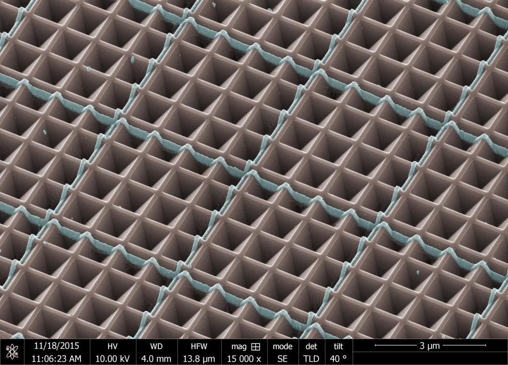
7 Substrate conformal imprint lithography PDMS Stamp Thin glass PDMS stamp (6 ) on 200 µm AF-45 glass 1 m Full-wafer soft nano-imprint Flexible rubber on thin glass Conform to substrate bow and roughness No stamp damage due to particles Marc Verschuuren PhD thesis, Utrecht University (2010)
 Si 3 N 4 Absorption (%) 80 60 40 20 flat coating")
 Piero Spinelli IEEE J. Photovolt.")
8 Light trapping in 5 m crystalline Si slab 100 FDTD simulation Mie (random) Si 3 N 4 Absorption (%) flat coating Mie (periodic) Si Back reflector t = 5µm Wavelength (nm) Piero Spinelli IEEE J. Photovolt. 4, 554 (2014)

9 Optimizing spatial frequency of scattering pattern Asahi U-type Claire van Lare ACS Photon. 2, 822 (2015)
10 Effect of EVA encapsulation Si EVA Si Piero Spinelli IEEE J. Photovolt. 5, 559 (2015)

11 TiO 2 nanoscatterers on Si Al 2 O 3 surface passivation TiO 2 Mie coating Si wafer ( = 3 ms) 5 nm Al 2 O 3 Bare Si wafer 5 nm Al 2 O % TiO 2 Mie coating 2.6% 1.6% Piero Spinelli, Bart Macco Appl. Phys. Lett. 102, (2013)

12 Nanopatterned Si solar cell designs Piero Spinelli, Bonna Newman

13 Ultra-thin a-si:h solar cell: 90 nm i layer 400 nm pitch Experiment patterned flat enhanced red and blue response by resonant dielectric Simulation scatterers 400 nm pitch 400 nm pitch flat flat 500 nm pitch 500 nm ITO pitch a-si:h ZnO:Al 500 nm Ag sol-gel Vivian Ferry, Claire van Lare Nano Lett. 11, 4239 (2011), Optics Express 21, (2013)

14 Nanopatterned CIGS solar cell designs TiO 2 AZO (240 nm) ITO (130 nm) CdS (100 nm) CIGS (460 nm) Mo (800 nm) nano nano + enhanced V oc flat flat reduced backrecombination Claire van Lare, Guanchao Yin ACS Nano 9, 9603 (2015)


15 Nanopatterned GaAs, thin crystalline Si simulations Piero Spinelli, Dennis Callahan, Lourens van Dijk

16 The solar cell as an optical integrated circuit =670 nm ITO a-si:h ZnO:Al Ag sol-gel 500 nm Vivian Ferry, Claire van Lare Nano Lett. 11, 4239 (2011), Optics Express 21, (2013)


17 Soft-imprinted nanopatterned AR interference coating Silica sol-gel Rubber stamp Nanoglass Flexible Silica nanopattern with effective index n= nm d = 240 nm h = 120 nm p = 325 nm Jorik van de Groep, Piero Spinelli Nano Lett. 15, 4223 (2015)
18 Measured total reflection Silica nanopattern on glass substrate 7.3 % 4.3 % 1.1 % Jorik van de Groep, Piero Spinelli Nano Lett. 15, 4223 (2015)
19 Nano-imprinted encapsulated Si solar cells 3.8% increase in photocurrent Jorik van de Groep, Piero Spinelli Nano Lett. 15, 4223 (2015)


20 Nano-imprinted smart phones flat patterned Jorik van de Groep, Piero Spinelli Nano Lett. 15, 4223 (2015)

21 Hydrophobicity Jorik van de Groep, Piero Spinelli Nano Lett. 15, 4223 (2015)


22 Transparent conductive silver nanowire network 2 m Ag nanowire network fabricated with electron beam lithography width: nm height: 60 nm Jorik van de Groep, Piero Spinelli Nano Lett. 12, 3138 (2012)


23 Transparent conductive silver nanowire network Optical transmission 45 nm 110 nm MIM plasmons Localized plasmons Surface plasmons I-V Ag nanowires can replace ITO Jorik van de Groep, Piero Spinelli Nano Lett. 12, 3138 (2012)
24 Ag nanowire network transparent conductors pitch 100 nm Ag nanowires on glass Jorik van de Groep, Dhritiman Gupta Sci. Rep. 5, (2015)
25 Metal nanowire printed Si HIT cells ITO: reduces J sc Ohmic losses Shading by Ag fingers Optical absorption Light reflection ITO dielectric function Drude absorption sunlight Ohmic losses shading ITO p+ a-si:h i a-si:h Ag fingers optical attenuation c-si wafer n type, FZ or CZ, <111> 50 µm 80 nm n interband absorption Wavelength (nm) k Synowicki, Thin Solid Films 313, 394 (1998) a-si:h i n+ a-si:h ITO Ag Mark Knight Jorik van de Groep


26 Metal nanowire printed Si HIT solar cells SCIL in silica sol-gel + Ag evaporation + lift-off Varying array pitch Width ~80 nm 1000 nm 800 nm 600 nm 400 nm Varying wire width Pitch 500 nm 63 nm 82 nm 101 nm 113 nm Mark Knight Jorik van de Groep
 chemically polished 5 mm")

27 SCIL on FZ and CZ Si wafers Float-zone Si(100) mechanically polished Czochralski-grown Si(111) chemically polished 5 mm Flexible PDMS stamp conforms to rough substrate No stamp damage due to dust, roughness Mark Knight Jorik van de Groep
 height (nm) 200 100 NW height: 50 nm 0 0 5 10 15 20 position ( m) Mark Knight Jorik van de Groep")
28 Nanoscale conformality of SCIL soft imprint Polished FZ Si Rough CZ Si height (nm) NW height: 50 nm position ( m) height (nm) NW height: 50 nm position ( m) Mark Knight Jorik van de Groep


29 Ag nanowire patterned Si heterojunction solar cells 80 nm ITO 20 nm ITO + Ag NW + SiNx Mark Knight, Jorik van de Groep, Paula Bronsveld


30 Ag nanowire patterned Si heterojunction solar cells NW pitch : 1 µm 2 µm 4 µm ITO only 1 cm 1 µm 80 nm ITO width: 80 nm height: 120 nm Mark Knight, Jorik van de Groep, Paula Bronsveld
31 Efficiency (%) FF J sc (ma cm -2 ) V oc (mw) Ag nanowire patterned Si heterojunction solar cells 1 µm 2 µm 4 µm no NW Mark Knight, Jorik van de Groep, Paula Bronsveld
32

")
33 Soft imprinted nanowire networks 100 nm Jorik van de Groep, Dhritiman Gupta Sci. Rep. 5, (2015)
 Jorik van de Groep, Matt Sheldon Science 346, 828")
34 Absorption cross section (10-19 cm 2 ) Plasmon resonance depends on charge density 20 nm Ag sphere in vacuum R p ne m e * 2 0 Wavelength (nm) Jorik van de Groep, Matt Sheldon Science 346, 828 (2014)
 F(")
 T N (nm) Jorik van de Groep, Matt Sheldon Science 346, 828")
35 Voltage (V) (nm) T(K) Plasmo-electric effect in metal nanostructures: thermodynamics Minimize free energy F(N,T) F( N, T) F F T N N T N T S N T N 0 0 o T/ N n/n 0 ( N, T) S( N, T) T N (nm) Jorik van de Groep, Matt Sheldon Science 346, 828 (2014)


36 Plasmo-electric potential: experiments Ag colloids on ITO Kelvin probe microscopy 60 nm Au Jorik van de Groep, Matt Sheldon Science 346, 828 (2014)
37 Plasmo-electric effect in metal nanostructures Jorik van de Groep, Matt Sheldon Science 346, 828 (2014)


38 Plasmo-electric effect on resonant Au hole arrays 100 mw/cm 2 Plasmo-electric potential spectral dependence shifts with array resonance Jorik van de Groep, Matt Sheldon Science 346, 828 (2014)

39 Plasmo-electric effect in metal nanostructures Jorik van de Groep, Matt Sheldon Science 346, 828 (2014)
40 Conclusions Light coupling and trapping Nanopatterned ARC on glass Transparent metal nanowire networks Plasmoelectric effect in metal nanostructures For details: see
PLASMONIC LIGHT TRAPPING FOR THIN FILM A-SI:H SOLAR CELLS
 PLASMONIC LIGHT TRAPPING FOR THIN FILM A-SI:H SOLAR CELLS VIVIAN E. FERRY 1,2, MARC A. VERSCHUUREN 3, HONGBO B. T. LI 4, EWOLD VERHAGEN 1, ROBERT J. WALTERS 1, RUUD E. I. SCHROPP 4, HARRY A. ATWATER 2,
DIELECTRIC nanoparticles (NPs) have recently been proposed
 have recently been proposed") IEEE JOURNAL OF PHOTOVOLTAICS 1 Effect of EVA Encapsulation on Antireflection Properties of Mie Nanoscatterers for c-si Solar Cells P. Spinelli, F. Lenzmann, A. Weeber, and A. Polman Abstract Dielectric
IEEE JOURNAL OF PHOTOVOLTAICS 1 Effect of EVA Encapsulation on Antireflection Properties of Mie Nanoscatterers for c-si Solar Cells P. Spinelli, F. Lenzmann, A. Weeber, and A. Polman Abstract Dielectric
CONFORMAL PLASMONIC A-SI:H SOLAR CELLS WITH NON-PERIODIC LIGHT TRAPPING PATTERNS
 CONFORMAL PLASMONIC A-SI:H SOLAR CELLS WITH NON-PERIODIC LIGHT TRAPPING PATTERNS Vivian E. Ferry 1,2, Marc A. Verschuuren 3, Claire van Lare 2, Ruud E. I. Schropp 4, Albert Polman 2, and Harry A. Atwater
Nanostrukturphysik (Nanostructure Physics)
") Nanostrukturphysik (Nanostructure Physics) Prof. Yong Lei & Dr. Yang Xu Fachgebiet 3D-Nanostrukturierung, Institut für Physik Contact: yong.lei@tu-ilmenau.de; yang.xu@tu-ilmenau.de Office: Unterpoerlitzer
Nanostrukturphysik (Nanostructure Physics) Prof. Yong Lei & Dr. Yang Xu Fachgebiet 3D-Nanostrukturierung, Institut für Physik Contact: yong.lei@tu-ilmenau.de; yang.xu@tu-ilmenau.de Office: Unterpoerlitzer
(Co-PIs-Mark Brongersma, Yi Cui, Shanhui Fan) Stanford University. GCEP Research Symposium 2013 Stanford, CA October 9, 2013
 Stanford University. GCEP Research Symposium 2013 Stanford, CA October 9, 2013") High-efficiency thin film nano-structured multi-junction solar James S. cells Harris (PI) (Co-PIs-Mark Brongersma, Yi Cui, Shanhui Fan) Stanford University GCEP Research Symposium 2013 Stanford, CA October
High-efficiency thin film nano-structured multi-junction solar James S. cells Harris (PI) (Co-PIs-Mark Brongersma, Yi Cui, Shanhui Fan) Stanford University GCEP Research Symposium 2013 Stanford, CA October
Embedded metallic nanopatterns for enhanced optical absorption
 Embedded metallic nanopatterns for enhanced optical absorption Fan Ye, Michael J. Burns, Michael J. Naughton* Department of Physics, Boston College, Chestnut Hill MA 02467 ABSTRACT Novel metallic nanopatterns
Controlling Fano lineshapes in plasmon-mediated light coupling into a substrate
 Controlling Fano lineshapes in plasmon-mediated light coupling into a substrate P. Spinelli,* C. van Lare, E. Verhagen, and A. Polman Center for Nanophotonics, FOM Institute AMOLF Science Park, 98 XG,
Light trapping using nanostructures offers
 Modeling Light Trapping in Nanostructured Solar Cells Vivian E. Ferry,,,, * Albert Polman, and Harry A. Atwater Thomas J. Watson Laboratories of Applied Physics, California Institute of Technology, Pasadena,
Light trapping in thin-film solar cells: the role of guided modes
 Light trapping in thin-film solar cells: the role of guided modes T. Søndergaard *, Y.-C. Tsao, T. G. Pedersen, and K. Pedersen Department of Physics and Nanotechnology, Aalborg University, Skjernvej 4A,
LIGHT TRAPPING IN SOLAR CELLS USING RESONANT NANOSTRUCTURES
 LIGHT TRAPPING IN SOLAR CELLS USING RESONANT NANOSTRUCTURES Cover image: Crystalline silicon solar cell with metal-wrap-through front-contact pattern (copyright ECN). A mirror image of the solar cell can
Simulations of solar cell absorption enhancement using resonant modes of a nanosphere array
 Green Photonics Award Paper Simulations of solar cell absorption enhancement using resonant modes of a nanosphere array Jonathan Grandidier* a, Michael G. Deceglie a, Dennis M. Callahan a, Harry A. Atwater
Simulations of solar cell absorption enhancement using resonant modes of a nanosphere array
 Simulations of solar cell absorption enhancement using resonant modes of a nanosphere array Jonathan Grandidier Michael G. Deceglie Dennis M. Callahan Harry A. Atwater Simulations of solar cell absorption
Light Trapping on Plasmonic-Photonic Nanostructured Fluorine- Doped Tin Oxide
 pubs.acs.org/jpcc Light Trapping on Plasmonic-Photonic Nanostructured Fluorine- Doped Tin Oxide Fengli Wang, Qian Wang, Guowei Xu, Rongqing Hui, and Judy Wu* The University of Kansas, Lawrence, Kansas
Fundamentals of Light Trapping
 Fundamentals of Light Trapping James R. Nagel, PhD November 16, 2017 Salt Lake City, Utah About Me PhD, Electrical Engineering, University of Utah (2011) Research Associate for Dept. of Metallurgical Engineering
Optimal-enhanced Solar Cell Ultra-thinning with Broadband Nanophotonic Light Capture
 Accepted Manuscript Optimal-enhanced Solar Cell Ultra-thinning with Broadband Nanophotonic Light Capture Manuel J. Mendes, Sirazul Haque, Olalla Sanchez-Sobrado, Andreia Araújo, Hugo Águas, Elvira Fortunato,
Light Absorption Enhancement in Thin-Film Solar Cells Using Whispering Gallery Modes in Dielectric Nanospheres
 Light Absorption Enhancement in Thin-Film Solar Cells Using Whispering Gallery Modes in Dielectric Nanospheres Jonathan Grandidier, * Dennis M. Callahan, Jeremy N. Munday, and Harry A. Atwater For thin-film
scattering patterns Center for Nanophotonics, FOM Institute AMOLF, Science Park 104, 1098 XG Amsterdam,
 Light coupling and trapping in ultra-thin Cu(In,Ga)Se 2 solar cells using dielectric scattering patterns M.-Claire van Lare,, Guanchao Yin,, Albert Polman, and Martina Schmid,, Center for Nanophotonics,
6 Correlation between the surface morphology and the current enhancement in n-i-p silicon solar cells
 6 Correlation between the surface morphology and the current enhancement in n-i-p silicon solar cells 6.1 Introduction In order to enhance the generated photocurrent in thin microcrystalline silicon solar
High resolution THz scanning for optimization of dielectric layer opening process on doped Si surfaces
 High resolution THz scanning for optimization of dielectric layer opening process on doped Si surfaces P. Spinelli 1, F.J.K. Danzl 1, D. Deligiannis 1,2, N. Guillevin 1, A.R. Burgers 1, S. Sawallich 3,
ALIGNMENT ACCURACY IN A MA/BA8 GEN3 USING SUBSTRATE CONFORMAL IMPRINT LITHOGRAPHY (SCIL)
") ALIGNMENT ACCURACY IN A MA/BA8 GEN3 USING SUBSTRATE CONFORMAL IMPRINT LITHOGRAPHY (SCIL) Robert Fader Fraunhofer Institute for Integrated Systems and Device Technology (IISB) Germany Ulrike Schömbs SUSS
ALIGNMENT ACCURACY IN A MA/BA8 GEN3 USING SUBSTRATE CONFORMAL IMPRINT LITHOGRAPHY (SCIL) Robert Fader Fraunhofer Institute for Integrated Systems and Device Technology (IISB) Germany Ulrike Schömbs SUSS
Plasmon enhancement of optical absorption in ultra-thin film solar cells by rear located aluminum nanodisk arrays
 Opt Quant Electron (2017)49:161 DOI 10.1007/s11082-017-0930-x Plasmon enhancement of optical absorption in ultra-thin film solar cells by rear located aluminum nanodisk arrays Debao Zhang 1 Yawei Kuang
Nanophotonic resonators for InP solar cells
 Nanophotonic resonators for InP solar cells Daniel A. Goldman, 1,2 Joseph Murray, 1,2 and Jeremy N. Munday 1,2,* 1 Department of Electrical and Computer Engineering, University of Maryland, College Park,
NSF EPSCoR Kansas Center for Solar Energy Research Annual Program Review June 12-14, 2011
 NSF EPSCoR Kansas Center for Solar Energy Research Annual Program Review June 12-14, 2011 Plasmonic and Photonic Photovoltaics based on graphene and other carbon nanostructures Fengli Wang, Guowei Xu,
Invited Paper ABSTRACT 1. INTRODUCTION
 Invited Paper Numerical Prediction of the Effect of Nanoscale Surface Roughness on Film-coupled Nanoparticle Plasmon Resonances Chatdanai Lumdee and Pieter G. Kik *,, CREOL, the College of Optics and Photonics;
Plasmonic Hot Hole Generation by Interband Transition in Gold-Polyaniline
 Supplementary Information Plasmonic Hot Hole Generation by Interband Transition in Gold-Polyaniline Tapan Barman, Amreen A. Hussain, Bikash Sharma, Arup R. Pal* Plasma Nanotech Lab, Physical Sciences Division,
Mesoporous titanium dioxide electrolyte bulk heterojunction
 Mesoporous titanium dioxide electrolyte bulk heterojunction The term "bulk heterojunction" is used to describe a heterojunction composed of two different materials acting as electron- and a hole- transporters,
B eing the dominant products on the photovoltaic market, crystalline Si wafer solar cells have been the
 OPEN SUBJECT AREAS: NANOPHOTONICS AND PLASMONICS NANOPARTICLES SOLAR CELLS Towards ultra-thin plasmonic silicon wafer solar cells with minimized efficiency loss Yinan Zhang 1, Nicholas Stokes 1, Baohua
Nanomaterials and their Optical Applications
 Nanomaterials and their Optical Applications Winter Semester 2012 Lecture 08 rachel.grange@uni-jena.de http://www.iap.uni-jena.de/multiphoton Outline: Photonic crystals 2 1. Photonic crystals vs electronic
Bulk crystalline silicon (c-si) solar cells dominate the
 solar cells dominate the") pubs.acs.org/nanolett Efficient Light Trapping in Inverted Nanopyramid Thin Crystalline Silicon Membranes for Solar Cell Applications Anastassios Mavrokefalos, Sang Eon Han, Selcuk Yerci, Matthew S. Branham,
pubs.acs.org/nanolett Efficient Light Trapping in Inverted Nanopyramid Thin Crystalline Silicon Membranes for Solar Cell Applications Anastassios Mavrokefalos, Sang Eon Han, Selcuk Yerci, Matthew S. Branham,
Light trapping in ultrathin silicon photonic crystal superlattices with randomly-textured dielectric incouplers
 Light trapping in ultrathin silicon photonic crystal superlattices with randomly-textured dielectric incouplers Dennis M. Callahan, 1,* Kelsey A. W. Horowitz, 1 and Harry A. Atwater 1 1 Thomas J. Watson
Plasmonic Photovoltaics Harry A. Atwater California Institute of Technology
 Plasmonic Photovoltaics Harry A. Atwater California Institute of Technology Surface plasmon polaritons and localized surface plasmons Plasmon propagation and absorption at metal-semiconductor interfaces
Supporting Information
 Electronic Supplementary Material (ESI) for Nanoscale. This journal is The Royal Society of Chemistry 215 Supporting Information Enhanced Photovoltaic Performances of Graphene/Si Solar Cells by Insertion
High transmission nanowire contact arrays with subwavelength spacing
 reprint Phys. Status Solidi RRL 10, No. 2, 164 167 (2016) / DOI 10.1002/pssr.201510367 High transmission nanowire contact arrays with subwavelength spacing Etor San Román 1, Alan Vitrey 1, Jerónimo Buencuerpo
Development of active inks for organic photovoltaics: state-of-the-art and perspectives
 Development of active inks for organic photovoltaics: state-of-the-art and perspectives Jörg Ackermann Centre Interdisciplinaire de Nanoscience de Marseille (CINAM) CNRS - UPR 3118, MARSEILLE - France
Efficient Light Trapping in Inverted Nanopyramid Thin Crystalline Silicon Membranes for Solar Cell Applications
 Efficient Light Trapping in Inverted Nanopyramid Thin Crystalline Silicon Membranes for Solar Cell Applications The MIT Faculty has made this article openly available. Please share how this access benefits
Photovoltaic cell and module physics and technology
 Photovoltaic cell and module physics and technology Vitezslav Benda, Prof Czech Technical University in Prague benda@fel.cvut.cz www.fel.cvut.cz 6/21/2012 1 Outlines Photovoltaic Effect Photovoltaic cell
Date This document is downloaded from the Digital Open Access Repository of VTT. VTT P.O. box 1000 FI VTT Finland
 This document is downloaded from the Digital Open Access Repository of VTT Title Influence of Substrate on Plasmon-Induced Absorption Enhancements Author(s) Tappura, Kirsi; Luomahaara, Juho; Haatainen,
Research Article Enhanced Light Trapping in Thin Film Solar Cells Using a Plasmonic Fishnet Structure
 Photoenergy Volume 25, Article ID 969, 8 pages http://dx.doi.org/.55/25/969 Research Article Enhanced Light Trapping in Thin Film Solar Cells Using a Plasmonic Fishnet Structure Sayan Seal, Vinay Budhraja,
Strong Absorption in a 2D Materials-based Spiral Nanocavity
 1858 PIERS Proceedings, Prague, Czech Republic, July 6 9, 2015 Strong Absorption in a 2D Materials-based Spiral Nanocavity Mohammad H. Tahersima and Volker J. Sorger Department of Electrical and Computer
OPTO-ELECTRONIC MODELLING OF THIN FILM NANOCRYSTALLINE SILICON SOLAR CELLS
 Journal of Ovonic Research Vol. 8, No. 4, July - August 2012, p. 81-90 OPTO-ELECTRONIC MODELLING OF THIN FILM NANOCRYSTALLINE SILICON SOLAR CELLS S.N. AGBO a, P.E. UGWUOKE a, F.I. EZEMA b a National Centre
Surface plasmon waveguides
 Surface plasmon waveguides Introduction Size Mismatch between Scaled CMOS Electronics and Planar Photonics Photonic integrated system with subwavelength scale components CMOS transistor: Medium-sized molecule
Fabrication at the nanoscale for nanophotonics
 Fabrication at the nanoscale for nanophotonics Ilya Sychugov, KTH Materials Physics, Kista silicon nanocrystal by electron beam induced deposition lithography Outline of basic nanofabrication methods Devices
Supplementary Figure 1 XRD pattern of a defective TiO 2 thin film deposited on an FTO/glass substrate, along with an XRD pattern of bare FTO/glass
 Supplementary Figure 1 XRD pattern of a defective TiO 2 thin film deposited on an FTO/glass substrate, along with an XRD pattern of bare FTO/glass and a reference pattern of anatase TiO 2 (JSPDS No.: 21-1272).
arxiv: v2 [physics.optics] 11 Apr 2014
![arxiv: v2 [physics.optics] 11 Apr 2014](/thumbs/95/126501682.jpg "arxiv: v2 [physics.optics] 11 Apr 2014") Multilayer nanoparticle arrays for broad spectrum absorption enhancement in thin film solar cells arxiv:1312.0710v2 [physics.optics] 11 Apr 2014 Aravind Krishnan, 1, Snehal Das, 1 Siva Rama Krishna, 1
Multilayer nanoparticle arrays for broad spectrum absorption enhancement in thin film solar cells arxiv:1312.0710v2 [physics.optics] 11 Apr 2014 Aravind Krishnan, 1, Snehal Das, 1 Siva Rama Krishna, 1
AS high-efficiency solar cell technologies mature, harvesting
 1292 IEEE JOURNAL OF PHOTOVOLTAICS, VOL. 3, NO. 4, OCTOBER 2013 Evaluating Plasmonic Light Trapping With Photoluminescence Chog Barugkin, Yimao Wan, Daniel Macdonald, Senior Member, IEEE, and Kylie R.
Amorphous silicon thin film solar cells with engineered nanoparticles
 Amorphous silicon thin film solar cells with engineered nanoparticles A thesis submitted for the degree of Doctor of Philosophy by Boyuan Cai Principal Supervisor: Associate Professor Baohua Jia Coordinating
Design of 4-terminal solar modules combining thin-film wide-bandgap top cells and c-si bottom cells Zhang, D.; Soppe, W.; Schropp, R.E.I.
 Design of 4-terminal solar modules combining thin-film wide-bandgap top cells and c-si bottom cells Zhang, D.; Soppe, W.; Schropp, R.E.I. Published in: Energy Procedia DOI: 10.1016/j.egypro.2015.07.071
Optimizing the performance of metal-semiconductor-metal photodetectors by embedding nanoparticles in the absorption layer
 Journal of Electrical and Electronic Engineering 2015; 3(2-1): 78-82 Published online February 10, 2015 (http://www.sciencepublishinggroup.com/j/jeee) doi: 10.11648/j.jeee.s.2015030201.27 ISSN: 2329-1613
High Efficiency Triple-Junction Solar Cells Employing Biomimetic Antireflective Structures
 High Efficiency Triple-Junction Solar Cells Employing Biomimetic Antireflective Structures M.Y. Chiu, C.-H. Chang, F.-Y. Chang, and Peichen Yu, Green Photonics Laboratory Department of Photonics National
Photonic crystals. Semi-conductor crystals for light. The smallest dielectric lossless structures to control whereto and how fast light flows
 Photonic crystals Semi-conductor crystals for light The smallest dielectric lossless structures to control whereto and how fast light flows Femius Koenderink Center for Nanophotonics AMOLF, Amsterdam f.koenderink@amolf.nl
EE 5611 Introduction to Microelectronic Technologies Fall Tuesday, September 23, 2014 Lecture 07
 EE 5611 Introduction to Microelectronic Technologies Fall 2014 Tuesday, September 23, 2014 Lecture 07 1 Introduction to Solar Cells Topics to be covered: Solar cells and sun light Review on semiconductor
Dielectric Meta-Reflectarray for Broadband Linear Polarization Conversion and Optical Vortex Generation
 Supporting Information Dielectric Meta-Reflectarray for Broadband Linear Polarization Conversion and Optical Vortex Generation Yuanmu Yang, Wenyi Wang, Parikshit Moitra, Ivan I. Kravchenko, Dayrl P. Briggs,
Design Considerations for Plasmonic Photovoltaics
 Design Considerations for Plasmonic Photovoltaics By Vivian E. Ferry, Jeremy N. Munday, and Harry A. Atwater * This paper reviews the recent research progress in the incorporation of plasmonic nanostructures
Demonstration of Near-Infrared Negative-Index Materials
 Demonstration of Near-Infrared Negative-Index Materials Shuang Zhang 1, Wenjun Fan 1, N. C. Panoiu 2, K. J. Malloy 1, R. M. Osgood 2 and S. R. J. Brueck 2 1. Center for High Technology Materials and Department
UvA-DARE (Digital Academic Repository) Resonant nanophotonic structures for photovoltaics van de Groep, J. Link to publication
 Resonant nanophotonic structures for photovoltaics van de Groep, J. Link to publication") UvA-DARE (Digital Academic Repository) Resonant nanophotonic structures for photovoltaics van de Groep, J. Link to publication Citation for published version (APA): van de Groep, J. (215). Resonant nanophotonic
UvA-DARE (Digital Academic Repository) Resonant nanophotonic structures for photovoltaics van de Groep, J. Link to publication Citation for published version (APA): van de Groep, J. (215). Resonant nanophotonic
Enhancement of optical absorption in thin-film solar cells through the excitation of higher-order nanoparticle plasmon modes
 Enhancement of optical absorption in thin-film solar cells through the excitation of higher-order nanoparticle plasmon modes Yu.A. Akimov 1,, W.S. Koh 1, and K. Ostrikov 2 1 Advanced Photonics and Plasmonics
Very large plasmon band shift in strongly coupled metal nanoparticle chain arrays.
 Mat. Res. Soc. Symp. Proc. Vol. 797 2004 Materials Research Society W4.6.1 Very large plasmon band shift in strongly coupled metal nanoparticle chain arrays. L. A. Sweatlock 1, J. J. Penninkhof 2, S. A.
Plasmonic Hole Arrays for Combined Photon and Electron Management
 Plasmonic Hole Arrays for Combined Photon and Electron Management Andreas C. Liapis, 1, a) Matthew Y. Sfeir, 1 1, b) and Charles T. Black Center for Functional Nanomaterials, Brookhaven National Laboratory,
Mie resonators on silicon Fabrication and optical properties
 Mie resonators on silicon Fabrication and optical properties Marco Abbarchi 1, Meher Naffouti 1,4, Thomas David 1, Benjamin Vial 2, Abdelmalek Benkouider 1, Laurent Lermusiaux 3,Luc Favre 1, Antoine Ronda
Carbon Nanotube Thin-Films & Nanoparticle Assembly
 Nanodevices using Nanomaterials : Carbon Nanotube Thin-Films & Nanoparticle Assembly Seung-Beck Lee Division of Electronics and Computer Engineering & Department of Nanotechnology, Hanyang University,
Nanophotonics: solar and thermal applications
 Nanophotonics: solar and thermal applications Shanhui Fan Ginzton Laboratory and Department of Electrical Engineering Stanford University http://www.stanford.edu/~shanhui Nanophotonic Structures Photonic
Lithography-Free Broadband Ultrathin Film. Photovoltaics
 Supporting Information Lithography-Free Broadband Ultrathin Film Absorbers with Gap Plasmon Resonance for Organic Photovoltaics Minjung Choi 1, Gumin Kang 1, Dongheok Shin 1, Nilesh Barange 2, Chang-Won
PHOTOVOLTAICS Fundamentals
 PHOTOVOLTAICS Fundamentals PV FUNDAMENTALS Semiconductor basics pn junction Solar cell operation Design of silicon solar cell SEMICONDUCTOR BASICS Allowed energy bands Valence and conduction band Fermi
High efficiency silicon and perovskite-silicon solar cells for electricity generation
 High efficiency silicon and perovskite-silicon solar cells for electricity generation Ali Dabirian Email: dabirian@ipm.ir 1 From Solar Energy to Electricity 2 Global accumulative PV installed In Iran it
1. Depleted heterojunction solar cells. 2. Deposition of semiconductor layers with solution process. June 7, Yonghui Lee
 1. Depleted heterojunction solar cells 2. Deposition of semiconductor layers with solution process June 7, 2016 Yonghui Lee Outline 1. Solar cells - P-N junction solar cell - Schottky barrier solar cell
Mode Splitting for Efficient Plasmoinc Thin-film Solar Cell
 Mode Splitting for Efficient Plasmoinc Thin-film Solar Cell Tong Li 1,*, Lei Dai 1, and Chun Jiang 1 1 State Key Laboratory of Advanced Optical Communication Systems and Networks, Shanghai Jiao Tong University,
Plasmon-Enhanced Light Absorption in GaAs Nanowire Array Solar Cells
 Li et al. Nanoscale Research Letters (2015) 10:436 DOI 10.1186/s11671-015-1110-1 NANO EXPRESS Plasmon-Enhanced Light Absorption in GaAs Nanowire Array Solar Cells Yanhong Li, Xin Yan, Yao Wu, Xia Zhang
CURRENT STATUS OF NANOIMPRINT LITHOGRAPHY DEVELOPMENT IN CNMM
 U.S. -KOREA Forums on Nanotechnology 1 CURRENT STATUS OF NANOIMPRINT LITHOGRAPHY DEVELOPMENT IN CNMM February 17 th 2005 Eung-Sug Lee,Jun-Ho Jeong Korea Institute of Machinery & Materials U.S. -KOREA Forums
Photovoltaic cell and module physics and technology. Vitezslav Benda, Prof Czech Technical University in Prague
 Photovoltaic cell and module physics and technology Vitezslav Benda, Prof Czech Technical University in Prague benda@fel.cvut.cz www.fel.cvut.cz 1 Outlines Photovoltaic Effect Photovoltaic cell structure
A normal-incident quantum well infrared photodetector enhanced by surface plasmon resonance
 Best Student Paper Award A normal-incident quantum well infrared photodetector enhanced by surface plasmon resonance Wei Wu a, Alireza Bonakdar, Ryan Gelfand, and Hooman Mohseni Bio-inspired Sensors and
Simulated Study of Plasmonic Coupling in Noble Bimetallic Alloy Nanosphere Arrays
 CHAPTER 4 Simulated Study of Plasmonic Coupling in Noble Bimetallic Alloy Nanosphere Arrays 4.1 Introduction In Chapter 3, the noble bimetallic alloy nanosphere (BANS) of Ag 1-x Cu x at a particular composition
Supplementary Information. Light Manipulation for Organic Optoelectronics Using Bio-inspired Moth's Eye. Nanostructures
 Supplementary Information Light Manipulation for Organic Optoelectronics Using Bio-inspired Moth's Eye Nanostructures Lei Zhou, Qing-Dong Ou, Jing-De Chen, Su Shen, Jian-Xin Tang,* Yan-Qing Li,* and Shuit-Tong
Photovoltaic Enhancement Due to Surface-Plasmon Assisted Visible-Light. Absorption at the Inartificial Surface of Lead Zirconate-Titanate Film
 Photovoltaic Enhancement Due to Surface-Plasmon Assisted Visible-Light Absorption at the Inartificial Surface of Lead Zirconate-Titanate Film Fengang Zheng, a,b, * Peng Zhang, a Xiaofeng Wang, a Wen Huang,
Optical cavity modes in gold shell particles
 9 Optical cavity modes in gold shell particles Gold (Au) shell particles with dimensions comparable to the wavelength of light exhibit a special resonance, with a tenfold field enhancement over almost
Supporting Information: Poly(dimethylsiloxane) Stamp Coated with a. Low-Surface-Energy, Diffusion-Blocking,
 Stamp Coated with a. Low-Surface-Energy, Diffusion-Blocking,") Supporting Information: Poly(dimethylsiloxane) Stamp Coated with a Low-Surface-Energy, Diffusion-Blocking, Covalently Bonded Perfluoropolyether Layer and Its Application to the Fabrication of Organic Electronic
Supporting Information: Poly(dimethylsiloxane) Stamp Coated with a Low-Surface-Energy, Diffusion-Blocking, Covalently Bonded Perfluoropolyether Layer and Its Application to the Fabrication of Organic Electronic
Supplementary information
 Supplementary information Neutral Colour Semitransparent Microstructured Perovskite Solar Cells Giles E. Eperon, Victor M. Burlakov, Alain Goriely and Henry J. Snaith 1. Controlling dewetting to achieve
Light Concentration in Polymer Bulk Heterojunction Solar Cells with Plasmonic Nanoparticles
 Light Concentration in Polymer Bulk Heterojunction Solar Cells with Plasmonic Nanoparticles Jinfeng Zhu* a, Baoqing Zeng* a, Richard S. Kim b, Zhe Wu a, a School of Physical Electronics, University of
A. Optimizing the growth conditions of large-scale graphene films
 1 A. Optimizing the growth conditions of large-scale graphene films Figure S1. Optical microscope images of graphene films transferred on 300 nm SiO 2 /Si substrates. a, Images of the graphene films grown
SUPPLEMENTARY INFORMATION
 SUPPLEMENTARY INFORMATION Nano-scale plasmonic motors driven by light Ming Liu 1, Thomas Zentgraf 1, Yongmin Liu 1, Guy Bartal 1 & Xiang Zhang 1,2 1 NSF Nano-scale Science and Engineering Center (NSEC),
II.2 Photonic Crystals of Core-Shell Colloidal Particles
 II.2 Photonic Crystals of Core-Shell Colloidal Particles We report on the fabrication and optical transmission studies of thin three-dimensional photonic crystals of high-dielectric ZnS-core and low-dielectric
Study of Silver Nanoparticles Electroless Growth and Their Impact on Silicon Properties
 Chemistry Journal Vol. 1, No. 3, 2015, pp. 90-94 http://www.publicscienceframework.org/journal/cj Study of Silver Nanoparticles Electroless Growth and Their Impact on Silicon Properties R. Benabderrahmane
Optical and Photonic Glasses. Lecture 39. Non-Linear Optical Glasses III Metal Doped Nano-Glasses. Professor Rui Almeida
 Optical and Photonic Glasses : Non-Linear Optical Glasses III Metal Doped Nano-Glasses Professor Rui Almeida International Materials Institute For New Functionality in Glass Lehigh University Metal-doped
ECE 695 Numerical Simulations Lecture 35: Solar Hybrid Energy Conversion Systems. Prof. Peter Bermel April 12, 2017
 ECE 695 Numerical Simulations Lecture 35: Solar Hybrid Energy Conversion Systems Prof. Peter Bermel April 12, 2017 Ideal Selective Solar Absorber Efficiency Limits Ideal cut-off wavelength for a selective
Surface Plasmon Polariton Assisted Metal-Dielectric Multilayers as Passband Filters for Ultraviolet Range
 Vol. 112 (2007) ACTA PHYSICA POLONICA A No. 5 Proceedings of the International School and Conference on Optics and Optical Materials, ISCOM07, Belgrade, Serbia, September 3 7, 2007 Surface Plasmon Polariton
Energy transport in metal nanoparticle plasmon waveguides
 Energy transport in metal nanoparticle plasmon waveguides Stefan A. Maier, Pieter G. Kik, and Harry A. Atwater California Institute of Technology Thomas J. Watson Laboratory of Applied Physics, Pasadena,
Enhanced Nonlinear Optical Response from Nano-Scale Composite Materials
 Enhanced Nonlinear Optical Response from Nano-Scale Composite Materials Robert W. Boyd The Institute of Optics, University of Rochester, Rochester, NY 14627, USA with special thanks to: Nick Lepeshkin,
Classical and Quantum Effects in Plasmonic Metals
 Classical and Quantum Effects in Plasmonic Metals Thesis by Ana Maii Brown In Partial Fulfillment of the Requirements for the degree of Doctor of Philosophy CALIFORNIA INSTITUTE OF TECHNOLOGY Pasadena,
Supplementary Figure S1. Hole collection layer photovoltaic performance in perovskite solar cells. Current voltage curves measured under AM1.
 Supplementary Figure S1. Hole collection layer photovoltaic performance in perovskite solar cells. Current voltage curves measured under AM1.5 simulated sun light at 100mWcm -2 equivalent irradiance for
3 Results and discussion
 Spray deposition of oxides at ambient atmosphere Part 2: Compact TiO 2 layers as a model for the investigation of an alternative solid state concept for dye solar cells F. Lenzmann Energy Research Centre
Organic solar cells. State of the art and outlooks. Gilles Horowitz LPICM, UMR7647 CNRS - Ecole Polytechnique
 Organic solar cells. State of the art and outlooks Gilles Horowitz LPICM, UMR7647 CNRS - Ecole Polytechnique Solar energy Solar energy on earth: 75,000 tep/year 6000 times the world consumption in 2007
Design guidelines for efficient plasmonic solar cells exploiting the trade-off between scattering and metallic absorption
 Design guidelines for efficient plasmonic solar cells exploiting the trade-off between scattering and metallic absorption Xiaofeng Li 1,2, *, Nicholas P. Hylton 3, Vincenzo Giannini 3, Ned J. Ekins-Daukes
Multicolor Graphene Nanoribbon/Semiconductor Nanowire. Heterojunction Light-Emitting Diodes
 Multicolor Graphene Nanoribbon/Semiconductor Nanowire Heterojunction Light-Emitting Diodes Yu Ye, a Lin Gan, b Lun Dai, *a Hu Meng, a Feng Wei, a Yu Dai, a Zujin Shi, b Bin Yu, a Xuefeng Guo, b and Guogang
Temperature Dependent Current-voltage Characteristics of P- type Crystalline Silicon Solar Cells Fabricated Using Screenprinting
 Temperature Dependent Current-voltage Characteristics of P- type Crystalline Silicon Solar Cells Fabricated Using Screenprinting Process Hyun-Jin Song, Won-Ki Lee, Chel-Jong Choi* School of Semiconductor
Supporting information for: Semitransparent Polymer-Based Solar Cells with. Aluminum-Doped Zinc Oxide Electrodes
 Supporting information for: Semitransparent Polymer-Based Solar Cells with Aluminum-Doped Zinc Oxide Electrodes Sebastian Wilken,, Verena Wilkens, Dorothea Scheunemann, Regina-Elisabeth Nowak, Karsten
Supplemental Discussion for Multijunction Solar Cell Efficiencies: Effect of Spectral Window, Optical Environment and Radiative Coupling
 Electronic Supplementary Material (ESI) for Energy & Environmental Science. This journal is The Royal Society of Chemistry 2014 Supplemental Discussion for Multijunction Solar Cell Efficiencies: Effect
Photonic crystals of core shell colloidal particles
 Letter to Appl. Phys. Letters June 8, 2001 Photonic crystals of core shell colloidal particles Krassimir P. Velikov, a, ) Alexander Moroz, a) and Alfons van Blaaderen a,b, ) a Physics and Chemistry of
International Journal of Nano Dimension
 ISSN: 2008-8868 Contents list available at IJND International Journal of Nano Dimension Journal homepage: www.ijnd.ir Short Communication Enhanced optical absorption in organic solar cells using metal
Advanced Texturing of Si Nanostructures on Low Lifetime Si Wafer
 Advanced Texturing of Si Nanostructures on Low Lifetime Si Wafer SUHAILA SEPEAI, A.W.AZHARI, SALEEM H.ZAIDI, K.SOPIAN Solar Energy Research Institute (SERI), Universiti Kebangsaan Malaysia (UKM), 43600
SUPPORTING INFORMATION
 SUPPORTING INFORMATION Non-Plasmonic SERS with Silicon: Is It Really Safe? New Insights into the Opto-Thermal Properties of Core/Shell Microbeads Nicolò Bontempi, a,d Irene Vassalini, a,b Stefano Danesi,
Spring 2009 EE 710: Nanoscience and Engineering
 Spring 009 EE 710: Nanoscience and Engineering Part 10: Surface Plasmons in Metals Images and figures supplied from Hornyak, Dutta, Tibbals, and Rao, Introduction to Nanoscience, CRC Press Boca Raton,