Characterization of Moisture and Thermally Induced Die Stresses in Microelectronic Packages
|
|
|
- Francis Simpson
- 5 years ago
- Views:
Transcription
1 Characterization of Moisture and Thermally Induced Die Stresses in Microelectronic Packages by Quang Nguyen A dissertation submitted to the Graduate Faculty of Auburn University in partial fulfillment of the requirements for the Degree of Doctor of Philosophy Auburn, Alabama December 16, 2017 Keywords: Die Stresses, Piezoresistive Stress Sensor, Moisture Effect, Hygroscopic Properties, Moisture Diffusion Simulation Copyright 2017 by Quang Nguyen Approved by Jeffrey C. Suhling, Chair, Quina Distinguished Professor of Mechanical Engineering Richard C. Jaeger, Emeritus Professor of Electrical Engineering Hareesh V. Tippur, McWane Professor of Mechanical Engineering James S. Davidson, Gottlieb Professor of Civil Engineering
2 Abstract Moisture has been one of the major concerns for package designers and reliability researchers. It is well-known that high humidity combined with high temperature can cause a number of failure modes to electronic devices, such as popcorn cracking, delamination, or electrochemical migration. While the fundamental knowledge of moisture effects on electronic packages has been extensively explored, it is still a challenge for researchers to fully understand the failure mechanisms associated with moisture or to numerically predict those failure modes due to the complexity of the moisture effects. In fact, it is believed that the moisture failure mechanism is the combination of material properties degradation, interfacial adhesion strength degradation, vapor pressure, and hygroscopic swelling. In this work, a study on hygroscopic properties of polymeric materials was conducted where diffusivity (D), saturated concentration (Csat) and coefficient of moisture expansion (CME) of underfill, BT substrate and molding compound were characterized. A novel methodology to measure CME was developed and successfully implemented using nanoindentation technology. A study on moisture desorption in polymeric materials was also completed. On-chip piezoresistive sensors were used to measure moisture-induced device side die stresses in Flip Chip on Laminate, Quad Flat Package (QFP) and Plastic Ball Grid Array Package (PBGA) under high humidity and high temperature conditions. The die stresses ii
3 were also monitored during the subsequent drying to evaluate the reversibility of the moisture effects. After the initial 10 days of moisture exposure, moisture was found to have significant effects on the package, generating tensile die normal stresses of up to 30, 120, and 35 MPa for Flip Chip, QFP and PBGA package respectively under 85 %RH, 85 C condition. Shear stresses however were found to be quite small relative to normal stresses. Upon the subsequent drying, it was seen in flip chip packages and PBGA package that the moisture-induced stress changes were almost fully recoverable while permanent changes in die stresses were found in QFP packages. In addition to the measurements of the moisture-induced die stresses, FEM moisture diffusion simulations were also performed to validate the experimental results. The hygroscopic properties obtained earlier were used for the FEM modeling. The numerical predictions were finally correlated with the experimental results. They were found to be in great agreement. The effects of temperature and humidity level on hygroscopic properties of polymeric materials were characterized. Diffusivities and saturated concentrations of three polymeric materials were determined at various moisture and temperature conditions ranging from 45 to 95 C and 45 to 95% RH. Valuable observations were made on the effects of temperature and humidity level on the hygroscopic properties of these three polymeric materials. Finally, an FEM parametric study was performed to characterize the dependence of moisture induced die stresses on three hygroscopic properties of polymeric materials in the packages. Insight into how moisture induced die stresses vary with each property was provided and this can be a great tool to predict the moisture induced die stresses and therefore offer the material selection to enhance the reliability of electronic packages iii
4 Acknowledgements First and foremost, I would like to express my deepest gratitude to my advisor, Dr. Jeffrey C. Suhling for the continuous support throughout my Ph.D study. Without his immense knowledge and great motivation, this dissertation would not have been completed. I truly grateful to Dr. Richard C. Jaeger, Dr. Hareesh V. Tippur and Dr. James S. Davidson for serving on my committee, giving tremendous guidance and valuable advice to widen my research from various perspectives. My appreciation is extended to Dr. Sa d Hamasha for serving as the university reader of this dissertation. My sincere thanks go to Dr. Jordan C. Roberts for his substantial help from the very first days of my graduate research in Auburn. I would like to thank my friends and lab mates, Bala, Vikas, Nolan, Nianjun, Safina, Hasnine, Basit vai, Shakil, Promode, Sudan, Sami, Fahim, Aminul, Rafidh, Jing, Chen, and Jun who made my experience in Auburn for the last four years really special and memorable. I would also like to take this opportunity to gratefully thank my brother, Dr. Tung Nguyen for his countless support and motivation during my entire graduate career. I am heartily thankful to my parents, Dien Nguyen and Hoa Hoang, my in-laws, Tuyen Le and Muoi Luong for their unconditional support, both spiritually and financially. Finally, I would like to acknowledge my wife Jasmine and my two wonderful little daughters, Daisy and Gemma. It is their love and inspiration that has kept me strong and motivated me to strive for excellence. iv
5 TABLE OF CONTENTS TABLE OF CONTENTS... v LIST OF TABLES... ix LIST OF FIGURES... x... 1 INTRODUCTION Literature Review Gaps in Literature and Objectives Organization of the Dissertation MEASUREMENT PROCEDURE Resistance Measurement for Stresses Determination Mass and Strain Measurement HYGROSCOPIC AND MECHANICAL PROPERTIES OF POLYMERIC MATERIALS Hygroscopic Properties v
6 3.2 Mechanical Properties MOISTURE INDUCED DIE STRESSES IN FLIP CHIP PACKAGES Introduction Test Vehicles Experimental Procedure and Results Correlation with FEM Simulation Summary and Conclusion MOISTURE INDUCED DIE STRESS IN QUAD FLAT PACKAGES Introduction Test Vehicles Experimental Procedure and Results Correlation with FEM Simulation Summary and Conclusion MOISTURE INDUCED DIE STRESS IN PLASTIC BGA PACKAGES Introduction Test Vehicles vi
7 6.3 Experimental Procedure and Results Correlation with FEM Simulation Summary and Conclusion MOISTURE DESORPTION OF POLYMERIC MATERIALS Experimental Procedure Desorption Diffusivity Fickian vs Non-Fickian Model Summary and Conclusion EFFECTS OF TEMPERATURE AND HUMIDITY LEVEL ON HYGROSCOPIC PROPERTIES OF POLYMERIC MATERIALS Experimental Procedure Summary and Conclusion PARAMETRIC STUDY ON THE DEPENDENCE OF MOISTURE INDUCED DIE STRESSES UPON HYGROSCOPIC PROPERTIES OF POLYMERIC MATERIALS IN ELECTRONIC PACKAGES Introduction Packages of Study Finite Element Models and Typical Package Behavior vii
8 9.4 Parametric Study Summary and Conclusion CONCLUSIONS AND FUTURE WORKS Conclusions Recommendations for Future Works REFERENCES viii
9 LIST OF TABLES Table 2.1: Bonding Pad and Scanner Card Connections Table 3.1: Diffusivity and Saturated Concentration Table 3.2: Hygroscopic Proprieties Table 3.3: Sample Dimension Table 3.4: Young Modulus and Poisson s Ratio Table 4.1: Hygroscopic Proprieties at 3 Conditions Table 4.2: Mechanical Proprieties Table 5.1: Material Properties Table 6.1: Material Properties Table 7.1: Desorption Diffusivity Table 7.2: Hygroscopic Properties Absorption and Desorption Table 7.3: Fickian and Non-Fickian Desorption Parameters at 175 and 210 C Table 8.1: Sample Dimensions Table 8.2: Test Protocol Table 8.3: Saturated Concentration of The Three Materials (mg/cm 3 ) Table 8.4: Diffusivities of The Three Materials (x10-8 cm 2 /s) Table 9.1: Material Properties of Quad Flat Package Table 9.2: Material Properties of Plastic Ball Grid Array Package Table 9.3: Material Properties of Flip Chip Package ix
10 LIST OF FIGURES Figure 1.1: Hierarchy of an Electronic Package... 2 Figure 1.2: The Most Common Interconnect Technologies... 3 Figure 1.3: Trend in Semiconductor Packaging... 4 Figure 1.4: Major Failure Modes of Solder Joints at Board Level Figure 1.5: Piezoresistive Sensor Concept... 8 Figure 1.6: Optimized Eight-Element Rosette on (111) Silicon... 9 Figure 2.1:Test Chip Software Logic Figure 2.2: Test Chip Measurement Software Interface Figure 2.3: Proper Biasing of Sensors Figure 2.4: Tenney Environmental Humidity/ Temperature System Figure 2.5: Flip Chip on Laminate Edge Connection Figure 2.6: Interface Board and Junction Box for Flip Chip on Laminate Measurement 27 Figure 2.7: CBGA Test Board Figure 2.8: QFP Socket and Test Board Connection Figure 2.9: PBGA Socket on Test Board Figure 2.10: Data Acquisition System Figure 2.11: Rosette Type 1 and Type Figure 2.12: Typical Wiring Diagram of Sensors used in JSE-WB Test Chips Figure 2.13: Bias for Resistance Measurements, Upper Arm of Half x
11 Figure 2.14: Bias for Resistance Measurements, Lower Arm of Half Bridge Figure 2.15: High Precision Electronic Scale Figure 2.16: TI 950 TriboIndenter System Figure 3.1: Mold Assembly and Final Underfill Specimen Figure 3.2: Original BT Board and Final Specimen Figure 3.3: Original Package with Mold Compound and Final Specimen Figure 3.4: Moisture Content vs Time of Underfill Figure 3.5: Moisture Content vs Time of BT Board Figure 3.6: Moisture Content vs Time of Mold Compound Figure 3.7: Moisture Content vs Time Correlation of Underfill Figure 3.8: Moisture Content vs Time Correlation of BT Board Figure 3.9: Moisture Content vs Time Correlation of Mold Compound Figure 3.10: Procedure of Coefficient 0f Moisture Expansion Determination Figure 3.11: Concentration and Strain_X Vs Time of Underfill Figure 3.12: CME_X Determination of Underfill Figure 3.13: Concentration and Strain_Y vs Time of Underfill Figure 3.14: CME_Y Determination of Underfill Figure 3.15: Concentration and Strain_X vs Time of BT Board Figure 3.16: CME_X Determination of BT Board Figure 3.17: Concentration and Strain_Y vs Time of BT Board Figure 3.18: CME_Y Determination of BT Board Figure 3.19: Concentration and Strain_X vs Time of Mold Compound xi
12 Figure 3.20: CME_X Determination of Mold Compound Figure 3.21: Concentration and Strain_Y vs Time of Mold Compound Figure 3.22: CME_Y Determination of Mold Compound Figure 3.23: Comparison of Diffusivity Figure 3.24: Comparison of Saturated Concentration Figure 3.25: Comparison of Coefficient of Moisture Expansion Figure 3.26: Strain Gages Mounting Figure 3.27: Microtester and Strain Gage Indicator System Figure 3.28: Young s Modulus and Poisson s Ratio Determination (Strain Gage Method) Figure 3.29: Specimens with Random Speckle Patterns Figure 3.30: DIC Test Setup Figure 3.31: DIC Test Procedure Figure 3.32: Young s Modulus and Poisson s Ratio Determination (DIC Method) Figure 3.33: FEM Model of Tensile Test Figure 3.34: Contour Plots of X and Y Displacements Figure 4.1: Stress Test Chips Figure 4.2: Test Board and Assembled FC400 Test Chip Figure 4.3: CBGA Package Assembly Figure 4.4: Experiment Protocol Figure 4.5: Die Normal Stresses after Underfill Curing Figure 4.6: Average Stress Variation with Long Term Aging xii
13 Figure 4.7: Die Stresses History Figure 4.8: Test Protocol Figure 4.9: Sample Weight Variation (85/85 Condition) Figure 4.10: Normal Stress Changes at Die Center (85/85 Condition) Figure 4.11: Normal Stress Changes at Die Corner (85/85 Condition) Figure 4.12: Comparison of Sample Weight Variation Figure 4.13: Comparison of Normal Stress 11 Changes at Die Center Figure 4.14: Comparison of Normal Stress 11 Changes at Die Corner Figure 4.15: Weight Gain Comparison Figure 4.16: Die Stresses Comparison Figure 4.17: Weight Gain During 4 Cycles Figure 4.18: Cyclic Normal Stress Variations at Die Center Figure 4.19: Cyclic Normal Stress Variations at Die Corner Figure 4.20: Quarter Model Finite Element Mesh and Detailed Views Figure 4.21: Moisture Loading on Underfill and BT Substrate Figure 4.22: Normal Stress Correlations after Underfill Figure 4.23: Sample Weight Gain Correlation Figure 4.24: Die Center Normal Stress 11 Correlations Figure 4.25: Die Center Normal Stress 11 Correlations Figure 4.26: Die Normal Stress 11 Correlation At 85/85 Condition Figure 4.27: Package and Die Displacement Figure 4.28: Moisture Concentration Evolution in the Underfill xiii
14 Figure 5.1: Stress Test Chips and Sensor Rosette Design Figure 5.2: Quad Flat Packages with Integral Stress Test Chips Figure 5.3: PCB and Socket for Resistance Measurements Figure 5.4: Stress Measurement Rosette Sites Figure 5.5: Die Stresses After Encapsulation Figure 5.6: Effects of Thermal Cycling on Die Stresses Figure 5.7: C-SAM Image of Delamination at Die Edge Figure 5.8: Average Stress Variation with Long Term Aging Figure 5.9: Experiment Protocol Figure 5.10: Sample Weight Variation Figure 5.11: Normal Stress Changes at Die Center Figure 5.12: Normal Stress Changes at Die Corner Figure 5.13: Expected Behavior of Die Stresses During Desorption Figure 5.14: Experiment Procedure to Explain Permanent Stress Change Figure 5.15:MC Weight Gain and Expansion During Absorption/ Desorption Figure 5.16: Shear Stress Changes at Die Center Figure 5.17: Shear Stress Changes at Die Corner Figure 5.18: Cross-Section Dimensions for QFP s Figure 5.19: FEM Meshing for Quarter Model Figure 5.20: Shear Stress Distribution Correlation Figure 5.21: Normal Stress Difference Distribution Correlation Figure 5.22: Shear Stress Distribution Correlation xiv
15 Figure 5.23: Shear Stress Distribution Correlation Figure 5.24: Finite Element Mesh (Quarter Model) Figure 5.25: Moisture Loading Boundary Conditions Figure 5.26: Sample Weight Gain Correlation Figure 5.27: Die Center Normal Stress Correlations Figure 5.28: Die Corner Normal Stress Correlations Figure 5.29: Moisture Concentration Evolution in the Mold Compound Figure 6.1: Stress Test Chips and Sensor Rosette Design Figure 6.2: PBGA Package Figure 6.3: PBGA Socket for Resistance Measurements Figure 6.4: Experiment Protocol Figure 6.5: Sample Weight vs. Humidity Exposure/Baking (5 x 5 mm Die) Figure 6.6: Normal Stress Changes at Die Center (5 x 5 mm Die) Figure 6.7: Normal Stress Changes at Die Corner (5 x 5 mm Die) Figure 6.8: Sample Weight vs. Humidity Exposure/Baking (10 x 10 mm Die) Figure 6.9: Normal Stress Changes at Die Center (10 x 10 mm Die) Figure 6.10: Average Normal Stress Changes at Die Corner (10 x 10 mm Die) Figure 6.11: Finite Element Mesh (5 x 5mm Die) Figure 6.12: Moisture Loading Boundary Conditions Figure 6.13: Sample Weight Gain Correlation (5 x 5 mm Die) Figure 6.14: Die Normal Stress Contour Correlation (5 x 5 mm) Figure 6.15: Die Center Normal Stress Correlation (5 x 5 mm) xv
16 Figure 6.16: Die Corner Normal Stress Correlation (5 x 5 mm) Figure 6.17: Sample Weight Gain Correlation (10 x 10 mm) Figure 6.18: Die Center Normal Stress Correlation (10x10 mm) Figure 6.19: Die Corner Normal Stress Correlation (10x10mm) Figure 6.20: Moisture Concentration Evolution in Molding Compound Figure 7.1: Testing Protocol Figure 7.2: Moisture Desorption for Underfill Figure 7.3: Moisture Desorption for BT Board Figure 7.4: Moisture Desorption for Mold Compound Figure 7.5: Desorption Diffusivity of Underfill Figure 7.6: Desorption Diffusivity of BT Board Figure 7.7: Desorption Diffusivity of Mold Compound Figure 7.8: Weight Variation Correlation of Underfill During 7 Days of Absorption and 100 Hours of Desorption Figure 7.9: Weight Variation Correlation of BT Board During 7 Days of Absorption and 100 Hours of Desorption Figure 7.10: Weight Variation Correlation of Mold Compound During 7 Days of Absorption and 100 Hours of Desorption Figure 7.11: Fickian and Non-Fickian Desorption of Underfill Figure 7.12: Fickian and Non-Fickian Desorption of BT Board Figure 7.13: Fickian and Non-Fickian Desorption of Mold Compound Figure 7.14: Comparison of Diffusivity Figure 7.15: Comparison of Saturated Concentration Figure 7.16: Comparison of Coefficient of Moisture Expansion xvi
17 Figure 8.1: Example of Data Processing7.2 Experimental Results Figure 8.2: Saturated Concentration of Underfill Figure 8.3: Saturated Concentration of BT Board Figure 8.4: Saturated Concentration of Mold Compound Figure 8.5: Saturated Concentration of Three Materials Figure 8.6: Diffusivity of Underfill Figure 8.7: Diffusivity of BT Board Figure 8.8: Diffusivity of Mold Compound Figure 8.9: Correlation of Moisture Content at 85% RH of Underfill Figure 8.10: Correlation of Moisture Content at 85% RH of BT Board Figure 8.11: Correlation of Moisture Content at 85% RH of Mold Compound Figure 9.1: Quad Flat Package Figure 9.2: Ball Grid Array Package Figure 9.3: Flip Chip on Laminate Package Figure 9.4: Quad Flat Package Model Figure 9.5: Ball Grid Array Package Model Figure 9.6: Flip Chip on Laminate Package Model Figure 9.7: Warpage of PBGA Package Figure 9.8: Die Stress in X-direction of PBGA Package (Moisture vs Thermal Load). 181 Figure 9.9: Weight Gain vs Time of PBGA Package Figure 9.10: Die Stresses in X Direction of PBGA Package Figure 9.11: Parametric Study on QFP xvii
18 Figure 9.12: Parametric Study on QFP Results Figure 9.13: Parametric Study on Flip Chip Figure 9.14: Parametric Study on Flip Chip - Results Figure 9.15: Parametric Study on PBGA Package Figure 9.16: Parametric Study on PBGA Package - Results xviii
19 INTRODUCTION 1.1 Literature Review In the following, the literature review for the current research is provided in four parts. In the first part, reliability in electronic packaging is discussed. An overview of electronic packaging is presented, following by the most typical types of package in the industry and finally the failure mechanisms mostly seen in electronic packages. The second part presents the piezoresistive sensor technology used in the study for the die stresses measurement. Next, the failure modes induced by moisture is discussed in part three. In part four, hygroscopic properties of polymeric materials available in literature are summarized. Finally, FEM simulation of moisture diffusion is reviewed Reliability in Electronic Packaging Electronic Packaging is an art of establishing interconnections between various layers of electrical devices, components, modules, and system. Packaging functions include electrical interconnection, power distribution, mechanical interconnection, heat dissipation, space transformer, and device protection from the environment, mechanical damage and light. It is a multidisciplinary process consisting of many different steps such as design, product development, and manufacture. In an electronic package, there can be many different levels of interconnect. The first three levels of interconnect are described 1
![in Figure 1.1 [1].](/docs-images/90/103029727/images/20-0.jpg "The first level of interconnect is the one between silicon chip(s) and chip carriers; the second level connects chip carriers with printed circuit board (PCB), while the third level connects PCB and")
![mother board. Figure 1.1: Hierarchy of an Electronic Package Wire bonding, Tape Automated Bonding (TAB) and solder bumping are the most common interconnect technologies (Figure 1.2) [1-2].](/docs-images/90/103029727/images/20-1.jpg "Among these technologies, solder bumping offers a variety of benefits including thermal and electrical performance, the highest input output (IO) density, substrate flexibility.")
20 in Figure 1.1 [1]. The first level of interconnect is the one between silicon chip(s) and chip carriers; the second level connects chip carriers with printed circuit board (PCB), while the third level connects PCB and mother board. Figure 1.1: Hierarchy of an Electronic Package Wire bonding, Tape Automated Bonding (TAB) and solder bumping are the most common interconnect technologies (Figure 1.2) [1-2]. Among these technologies, solder bumping offers a variety of benefits including thermal and electrical performance, the highest input output (IO) density, substrate flexibility. Wire bonding technology is relatively low cost; however, it has limited application. In wire bonded packages, lesser heat is dissipated to the surroundings through molding compound because of the low thermal conductivity of molding compound. 2
, Thin Small Outline Package (TSOP), Plastic Quad Flat")
21 Figure 1.2: The Most Common Interconnect Technologies Figure 1.3 shows the evolution of package type. In first evolution of package development, there is a trend changing from insertion-type to surface mounting, such as Dual Inline Packaging (DIP), Thin Small Outline Package (TSOP), Plastic Quad Flat Pack (PQFP). The second evolution is highlighted by changing from a package surrounded by leads to mounted ball terminals. The principal packaging types for this stage are Ball Grid Array (BGA) and Chip Scale Package (CSP). 3D packaging approaches such as SiP (System in Package), SoC (System on Chip) and SoP (System on Package) are emerging technologies in order to answer the requirements for smaller footprint, shorter interconnects and higher performance. The 3D packaging with through silicon via (TSV) technology is considered the next generation packaging solution. 3
![Figure 1.3: Trend in Semiconductor Packaging An electronic package can be affected by a number of factors [1-4].](/docs-images/90/103029727/images/22-0.jpg "These effects can lead to various reliability issues of the electronic package.")


22 Figure 1.3: Trend in Semiconductor Packaging An electronic package can be affected by a number of factors [1-4]. These effects can lead to various reliability issues of the electronic package. A failure mode of an electronic component represents a change of its functional status, such as open, short, change of resistance, capacitance, or other electrical parameters. Failure mechanisms have been classified by Dasgupta et al. [5], based on the rate of damage accumulation. Failure mechanisms fall into two broad categories: over-stress and wearout. Over-stress failures are instantaneous and catastrophic. Wearout failures accumulate damage incrementally over a long period, often leading first to performance degradation and then to device failure. Further classification of failure mechanisms is based on the type of load that triggers the mechanisms: mechanical (overstress, creep, fatigue, delamination), electrical 4
23 (electromigration, electrostatic discharge, electrical overstress), chemical (corrosion, contamination, diffusion) or radiation. The packaging process starts with back-grinding the wafer to a specified thickness followed by wafer dicing into individual die. A die is then attached to the lead frame using a die-attach adhesive. Nguyen et al. [6] has presented reliability issues in die attach process in a typical overmolded packages. The die attach process may cause die cracking [7-11]. The silicon die contracts less than the lead frame due to its smaller coefficient of thermal expansion (CTE) as the package is cooled to room temperature, resulting in bending of the die/lead frame structure. This bending may cause on-chip passivation and die cracking. Cracks typically initiate from the bottom of the die near the die edges and corners. For wire-bonding packages, wire-bonding will be done to provide interconnections from the die to the lead frame. Wire bond failures typically include fracture of the wire, shearing of the wire off the ball, and shearing the ball off the die surface. Koch et al.[12] found most of the bad bonds occurred on the side of the package opposite the mold compound injection gate. Nguyen et al. [13] found a very high transfer molding pressure is known to cause wire sweep failure. One of the most common sources of wire bond failures occurs as a consequence of attempts to relieve die surface stress by the use of compliant coatings on the top surface of the die. These coatings are typically soft-gel like materials such as silicone gel. These solutions help to alleviate die stresses but lead to an increase in wire bond failures [14-17]. 5
.")
![Among various failure mechanisms associated with the first failure mode, thermal fatigue is the primary one that cause electronics packages to fail [1-4].](/docs-images/90/103029727/images/24-1.jpg "Fatigue in solder alloys is a complex process of interaction between fatigue mechanisms driven by plastic deformation and creep deformation that occur during cyclic loading of the solder joints.")
24 For BGA packages, there are two major failure modes of solder joints at board level (Figure 1.4). The first mode is the failure in bulk solder; the second mode is the failure in intermetallic layer. The major failure mechanisms associated with the first mode is thermal fatigue damage (wearout mechanism). Among various failure mechanisms associated with the first failure mode, thermal fatigue is the primary one that cause electronics packages to fail [1-4]. Fatigue in solder alloys is a complex process of interaction between fatigue mechanisms driven by plastic deformation and creep deformation that occur during cyclic loading of the solder joints. Under cyclic loading of a printed wiring board assembly, repeated deformation of the solder joints results in the accumulation of fatigue damage. Cracks will nucleate and grow through the joint under the influence of cyclic loads. Figure 1.4: Major Failure Modes of Solder Joints at Board Level. Encapsulation in plastic packaging process can also cause many issues for the packages. The entire structure is encapsulated with a thermoset material referred to mold 6
25 compound. These compounds are comprised of epoxy resin and silica particles. This encapsulation generates different thermal stresses level within a plastic package based on the mold compound composition and properties [18-22] and may lead to passivation cracking in the die surface [23-28]. The primary issue with the mold compound is that it absorbs moisture over time. A delamination occurring between the backside of the die and the plastic provides a site for absorbed moisture to accumulate. During reflow processes, accumulated moisture vaporizes resulting in the generation of steam and a buildup of pressure between the backside of the die paddle and the plastic [29] causing the delamination to grow to the edges of the die paddle and cracks to extend from the edges of the paddle to the exterior of the package. This phenomenon is known as popcorn failure Piezoresistive Sensor Technology As illustrated in Figure 1.5, piezoresistive sensors can be used to characterize the stress distributions in packaged semiconductor die [30-32]. The resistive sensors are conveniently fabricated into the surface of the die using current microelectronic technology. The sensors are not mounted on the chips. Rather, they are an integral part of the structure (chip) to be analyzed by the way of the fabrication process. In conductors such as silicon that exhibit the piezoresistive effect, the electrical resistivity changes when the material is subjected to stress or pressure, which leads to measurable resistance changes in the rosette elements. Therefore, piezoresistive sensors are capable of providing nonintrusive measurements of surface stress states in packaged chips. If the piezoresistive sensors are calibrated over a wide temperature range, thermally induced stresses can be 7
![measured. For example, measurements have been made during encapsulant curing and assembly cooldown [33-34], as well as during thermal cycling reliability testing [35-39].](/docs-images/90/103029727/images/26-0.jpg "On-chip sensors have also been shown to be excellent tools for monitoring delamination at the die to encapsulant interface [35, 37-38, 40].")
26 measured. For example, measurements have been made during encapsulant curing and assembly cooldown [33-34], as well as during thermal cycling reliability testing [35-39]. On-chip sensors have also been shown to be excellent tools for monitoring delamination at the die to encapsulant interface [35, 37-38, 40]. Finally, a full-field mapping of the stress distribution over the surface of a die can be obtained using specially designed test chips that incorporate an array of sensors rosettes [41]. Although resistor sensors have historically been the most popular for test chip applications, additional miniaturization can be realized using transistor (FET) sensors [42-45] and van der Pauw sensors [46]. Figure 1.5: Piezoresistive Sensor Concept The resistance change for a resistor in the (111) plane is dependent on all six of the unique stress components [30, 32, 47]. Therefore, the potential exists for developing a sensor rosette that can measure the complete three-dimensional state of stress at points on the surface of a silicon die. The (111) silicon eight-element dual polarity rosette in Figure 1.6 has been developed for this purpose. It has been optimized to measure all six stress components. 8
27 x 2 [112] R 4,n R 3,n R 2,n 45 R 5,p R 1,n x 1 [110] R 6,p 45 R R 8,p 7,p R 7,p R 8,p Figure 1.6: Optimized Eight-Element Rosette on (111) Silicon Four components can be measured in a temperature compensated manner where the stress can be calculated directly from the resistance change measurements without the need to know the temperature. The rosette can be readily calibrated using uniaxial and hydrostatic testing. A six-element rosette (without resistors oriented at -45 ) can also be used to extract the complete stress state. However, including the two extra resistors allows for more convenient bridge measurements of the resistance changes and better stress measurement localization [47]. The rosette in Figure 1.6 contains p-type and n-type sensor sets, each with resistor elements making angles of o 0, 45, 90 with respect to the 1 x -axis. Using general piezoresistive expressions for (111) silicon [18, 20, 30], the following expressions for individual stress components can be derived: 9
28 10 (1.1) ] B + B ) (B B ) + B 2[(B T 2 R R R R B T 2 R R R R B + ] B B ) + (B B B ) + (B B B ) 2[(B R R R R ) B (B R R R R B ) (B = n 3 p 2 p 1 p 3 n 2 n 1 p n 3 n p 3 n 1 p 2 p 3 n 2 p 3 p 1 n 3 p 1 p n 2 n p 2 p 3 11 ] B + B ) (B B ) + B 2[(B T 2 R R R R B T 2 R R R R B + ] B B ) + (B B B ) + (B B B ) 2[(B R R R R B ) (B R R R R B ) (B = n 3 p 2 p 1 p 3 n 2 n 1 p n 3 n p 3 n 1 p 2 p 3 n 2 p 3 p 1 n 3 p 1 p n 2 n p 2 p 3 22 ] B + B ) (B B ) + B 2[(B T 2 R R R R ) + B + (B T 2 R R R R + B ) (B = n 3 p 2 p 1 p 3 n 2 n 1 p n 2 n 1 n p 2 p 1 33 ] ) B B + (B ) B B + (B ) B B B 2[( R R R R ) B + (B R R R R ) B (B = ) B B + (B ) B B + (B ) B B (B R R R R ) B + (B R R R R ) B (B 8 2 = ) B B + (B ) B B + (B ) B B (B R R R R ) B (B R R R R ) B (B 8 2 = ] ) B B + (B ) B B + (B ) B B [( B R R R R ) B (B R R R R ) B (B = n 1 p 2 p 3 n 2 p 3 p 1 n 3 p 1 p n 2 n p 2 p 3 12 n 1 p 2 p 3 n 2 p 3 p 1 n 3 p 1 p n 2 n p 2 p 1 23 n 1 p 2 p 3 n 2 p 3 p 1 n 3 p 1 p n 2 n p 2 p 1 13 n 1 p 2 p 3 n 2 p 3 p 1 n 3 p 1 p n 2 n p 2 p
29 where 11, 22 and 33 are the normal stress components; 12, 13 and 23 are the shear stress components; 1, 2,... are the temperature coefficients of resistance; T = Tm - Tref is the difference between the measurement temperature and reference temperature (where the unstressed resistance R is measured); and B1, B2, B3 are a set of linearly independent temperature dependent combined piezoresistive coefficients. The combined piezoresistive coefficients are related to the standard piezoresistive coefficients of silicon using: B 1 = B 2 = B 3 = (1.2) Superscripts n and p are used on the combined piezoresistive coefficients in equation (1.1) to denote n-type and p-type resistors, respectively. From the expressions in equation (1.1), it is clear that the extraction of the three shear stresses,, from the measured resistance changes is temperature compensated (independent of T). Evaluation of the individual normal stress components requires measurement of the normalized resistance changes of the sensors and the temperature change T experienced by the sensing elements. The temperature coefficients of resistance 1, 2,... must also be known for each doping type. They can be obtained using thermal cycling calibration experiments where the resistances of the sensing elements are monitored as a function of temperature. The measured resistance change versus temperature response is fit with a general polynomial to extract the temperature 11
30 coefficients of resistance. Typically, only first and second order temperature coefficients are needed. Jaeger and coworkers [48-53] have previously discussed the difficulties in obtaining accurate temperature change values over the long time spans typical of measurements made with piezoresistive sensors. In addition, it has been demonstrated that temperature measurement errors of as little as 0.25 C can cause serious errors in the experimental values of the stresses extracted with non-temperature compensated formulas such as the first three expressions in equation (1.1). Thus, it has been recommended to restrict measurement efforts to temperature compensated stress combinations where the temperature coefficient of resistance terms cancel in the stress extraction equations. Besides the three shear stresses, the in-plane normal stress difference can be shown to be an additional temperature compensated quantity using the first two expressions in (1.1): p p R1 R3 n n R5 R7 (B3 B 2) (B3 B2) R1 R3 R5 R = (1.3) p p n p p n p p n [(B B )B3 + (B B )B2 + (B B ) B 1 ] The results in equations (1.1, 1.3) assume that the temperature coefficients of resistance are well matched for sensing elements of the same doping type. In addition, a calibration procedure must be performed to determine all six of the combined n piezoresistive parameters 1 n n p p p B, B 2, B 3, B 1, B 2, 3 B prior to using the sensor [30, 32, 47]. A combination of four-point bending testing (uniaxial stress) [54], wafer level flexing (biaxial stress) [55], and hydrostatic pressure testing (triaxial stress) [56] can be utilized to complete this task. 12
31 1.1.3 Moisture Induced Failures in Electronic Packages Many failures in microelectronic packages can be traced back to moisture. In general, there are three types of failure mechanisms when atmospheric moisture is absorbed into a microelectronics device. The most notorious failure mode is often referred to as popcorn phenomenon [57-60]. Packaged microelectronic devices are exposed to factory environment during manufacturing process. Moisture is absorbed into polymeric components in the bulk materials and along the interfaces. During reflow process (220 to 260 C within a few minutes), many mechanisms occur in the packages. Material strengths of polymeric component significantly decrease, especially below their glass transition temperatures. Also, the interfacial adhesions substantially degrade. Vapor pressure is built up inside the package. As a result, failure may occur when water vapor is suddenly released due to delamination and cracking. The second failure mode induced by moisture is hygroscopic swelling. Polymeric materials swell at different rates when subjected to moisture, generating hygroscopic mismatch strain. The hygroscopic mismatch strain at the interfaces in a package could be as high as the thermal mismatch strains [61-63]. As a consequence, warpage and delamination may occur, leading to failure of the devices. Many studies were done to explore the diffusion mechanism leading to the hygroscopic swelling of polymeric materials [61-65], hygroscopic swelling was investigated by the means of warpage measurement of Cu/EMC bimaterial beams [66]. The third failure mechanism is electrochemical migration (corrosion) [67-70]. The first type of corrosion is metal dendritic growth at the cathode side of the substrate surface when metal migrate from anode to cathode and lead to formation of anode-cathode short failure. The second type is 13
32 conductive anodic filament (CAF) growth, occurring when CAF grows from anode to cathode along the delamination caused by moisture absorption. There are three types of accelerated moisture sensitivity/reliability tests to characterize the effects of moisture in a plastic package [71]. The first type is moisture/reflow sensitivity test, this test has established all the testing conditions such as temperature, humidity level and exposure time for a package to satisfy before assessing the reliability under operation conditions. The second kind is highly accelerated stress test (HAST), the test accelerates moisture absorption into package components by raising temperature and humidity level. The third kind is biased temperature/ humidity (TH), used to evaluate the reliability of a powered device at an elevated temperature/ humidity Hygroscopic Properties of Polymeric Materials Moisture absorbed by microelectronic packages can cause significant change in properties of polymeric materials such as Young s modulus, glass transition temperature, CTE, creep rate, interfacial adhesion [72-74]. These changes in material properties play an important role in the failure of the package. He et al. investigated the real-time characterization of moisture absorption and desorption [75]. In order to tackle issues associated with moisture, it is critical to understand the response of the materials to moisture exposure. There are three properties that can represent the response of polymeric materials to moisture: Diffusivity (D), Saturated Concentration (Csat) and Coefficient of Moisture Expansion (). A number of studies have been done to characterize these three properties of polymeric materials [59, 61, 63, 74-80]. Moisture 14
33 behavior of polymeric material is mainly dominated by the diffusion of water. It has been widely studied by many researchers and for most cases, the rate of diffusion is believed to be constant (Fickian diffusion) [77]. The mechanisms of moisture diffusion have been explored in both absorption and desorption. It is believed that two mechanisms occur during moisture absorption process [66]. The first mechanism is the absorption of the water molecules in free volumes or voids inside the materials. The second one is the hydrogen bonding formation between the water molecules and the polymer chains. Absorption of moisture in mold compound was found to show a dual-stage non-fickian behavior. Many types of non-fickian moisture absorption were reported in literature [81-82]. Some non- Fickian models were suggested to better fit the experimental results. It is also vital to understand the moisture desorption behavior since moisture desorption takes place at reflow process when popcorn failure usually occurs. Also, packages are usually baked during the assembly to reduce the possibility of moisture induced failures. Assumed to follow Fickian diffusion law, desorption diffusivity can be predicted at different temperature by Arrhenius equation [76]. Saturated concentration is another moisture property of polymeric materials, representing the maximum amount of moisture a given volume of material can absorb. Saturated concentration is directly related to vapor pressure inside the material voids during reflow process. While diffusivity is widely known to be temperature dependent [82], saturated concentration of many polymeric materials is shown to be dependent on humidity level only. Coefficient of moisture expansion represents the linear relationship between the hygroscopic strain from the dimensional change and the moisture concentration. Moisture induced swelling of polymers is reported to be mainly 15
34 due to the hydrogen bonding during the moisture absorption [61]. Coefficient of moisture expansion has been usually obtained by relate the weight loss of a saturated sample during baking process to dimensional changes of the. In this method, the diffusion mechanism was assumed to be the same in both absorption and desorption. This assumption was proved to not always hold true. Therefore, methods to determine coefficient of moisture expansion during absorption instead of desorption should be used [66]. CME can be measured by many tools and techniques including bending cantilever method, micrometer, Michelson interferometry, TMA/ TGA (thermal mechanical analyzer/ thermal gravimetric analyzer), Moiré, DIC (digital image correlation) Moisture Diffusion FEM Simulation It is well-known that finite element simulation is a powerful tool to evaluate the effects of moisture on electronic package reliability. However, FEM simulation of moisture diffusion has always been a challenge due to the complication of diffusion mechanism and lack of hygroscopic properties of polymeric materials in literature. Also, moisture induced failures in microelectronic package often result from a combination of many effects such as material properties change, vapor pressure accumulation, adhesion strength degradation, delamination propagation [83]. A number of efforts have been done to develop an efficient numerical approach to tackle moisture related issues in electronic packages. Thermalmoisture analogy was conventionally used to analyze moisture properties for different packaging materials based on the similarity of governing differential equations of transient moisture diffusion and transient heat transfer analysis [59]. When two materials with 16
35 different saturated concentration are joined together, normalized approach was used for moisture diffusion simulation analysis to overcome the discontinuity at interfaces by introducing a new material property called solubility (S) [84-85]. Wong et al [86-87] introduced a new normalized variable called wetness which is defined as the ratio of the moisture concentration over the saturated moisture concentration. When ambient temperature/humidity changes with time, thermal-moisture analogy is no longer applicable. A so-called direct concentration approach is introduced in which moisture concentration is used directly as a basic field variable, which is discontinuous at interfaces. Constraint equations are applied at the interfaces to satisfy the continuity requirement [88-90]. 1.2 Gaps in Literature and Objectives Gaps in Literature Piezoresistive sensor technology has never been used for moisture-induced die stresses measurements. Effects of moisture on die stresses which can be used to predict moisture induced failure mechanism such as delamination have not been studied. Effects of room temperature aging/ moisture cycling on die stresses has never been done. Complete sets of hygroscopic and mechanical properties of polymeric materials needed for numerical simulation of moisture diffusion are still limited. 17
36 An efficient approach to measure in-plane coefficient of moisture expansion (CME) in absorption process is not available. A deeper study on the effects of temperature and humidity level on the hygroscopic properties of polymeric materials is needed. A numerical study on real microelectronic packages to characterize die stresses induced by moisture diffusion has been not performed. The dependence of the moisture effects (weight gains, die stresses) upon each moisture property of polymeric components of electronic packages has never been explored Objectives Study the effects of moisture absorption/ desorption on the die stresses using piezoresistive sensor technology on three types of package - Flip chip on laminate, flip chip on ceramic ball grid array packages (CBGA) - Quad Flat Package (QFP) - Plastic Ball Grid Array Packages (PBGA) Determine hygroscopic properties of polymeric materials (BT board, underfill and mold compound) - Diffusivity - Saturated concentration Develop a new method to obtain coefficient of moisture expansion (CME) by using nanoindentation technology 18
37 Characterize the desorption diffusivities of polymeric materials Perform moisture diffusion simulations on 3 types of packages and correlate the experimental results with numerical prediction Study the dependence of the moisture effects (weight gains, die stresses) upon each moisture property of polymeric components of electronic packages Study the effects of temperature and humidity level on the hygroscopic properties of polymeric materials Determine mechanical properties of polymeric materials using two approaches (strain gages and DIC) - Young s modulus - Poisson s ratio 1.3 Organization of the Dissertation This dissertation is organized into nine chapters as follows: Chapter 1: Introduction and literature review Chapter 2: Measurement procedure Chapter 3: Hygroscopic and mechanical properties of polymeric materials Chapter 4: Moisture induced die stresses in flip chip packages Chapter 5: Moisture induced die stresses in Quad Flat Package (QFP) Chapter 6: Moisture induced die stresses in PBGA Packages Chapter 7: Moisture desorption on polymeric materials 19
38 Chapter 8: Effects of temperature and humidity level on hygroscopic properties of polymeric materials Chapter 9: Parametric study on the dependence of moisture induced die stresses upon hygroscopic properties of polymeric materials Chapter 10: Conclusions 20
39 MEASUREMENT PROCEDURE 2.1 Resistance Measurement for Stresses Determination Introduction The (111) silicon test chips used in this study were fabricated using six inch wafers and a bipolar process. The wafers were passivated using silicon nitride, and then redistributed and solder bumped. The resistances of sensors on each 20 x 20 mm test chip were characterized at several different points including as bare die, and after various packaging steps including die attachment, underfill application, and lid attachment. The hardware and software used to make resistance measurements were designed by several previous Auburn University students including Zou [40], Rahim [33], and H. Abdel-Hady. The utilized methods are briefly discussed below Resistance Measurement The Test Chip Software utilizes GPIB interface technology to control the data acquisition system used for resistance measurement of sensor rosettes. In this study, resistance measurements were made at multiple points of time. For studies on die stresses change with aging effects, initial resistance measurements were made years ago when the 21
40 packages were just assembled, and subsequent resistance were lately measured to extract the die stresses change with aging time under room temperature condition. For studies on moisture induced die stresses, initial resistance measurements were made before the sample were subjected to moisture, subsequent sets of resistance were measured during the moisture exposures to obtain the die stress chance with moisture effects Measurement Equipment The following is a list of equipment used for test measurement, as well as a description of how each item was used. Computer A PC-based computer and a custom National Instruments LabView software program were used to control the data acquisition process. A logic chart and the program interface are shown in Figures 2.1 and 2.2, respectively. Keithley 7002 Switch System Upon prompting from the control program, the switch turns on or off multiple channels in order to measure the resistance of successive resistors. Nine scanner cards were required for measurement of all of the devices on the test chip in this work. HP Multimeter #1 This multimeter measures current through a resistor. 22
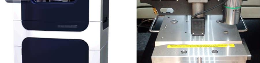
41 Power Supply During measurement of sensors, the power supply provides voltage to the measured resistors, and also provides bias in the circuit to prevent current leakage. For ease of resistance measurement, the voltage used is 1V. Figure 2.3 illustrates the proper biasing on n-type and p-type resistors. HP Multimeter #2 This multimeter measures the exact voltage across each resistor. A side advantage of using a second multimeter is that by comparing this voltage to the bias voltage, one can check the circuit. The voltage measured by this meter is used in the calculation of resistance. HP Multimeter #3 This meter measures the resistance value from a resistance thermometer, otherwise referred to as a thermistor. The thermistor is placed on the die to measure temperature changes needed for stress and TCR measurements. Tenney Environmental Humidity/Temperature Chamber (Model BTRS) The moisture exposure was performed in Tenney Environmental Humidity/ Temperature chamber with the temperature ranging from -34 to 200 C and the humidity level ranging from 20 to 98% RH (Figure 2.4) 23
42 Accessories For flip chip on laminate measurements, a pair of connectors were used to contact to gold plated tabs on the perimeter of the substrates (Figure 2.5). Ribbon cables and connectors were also needed to provide electrical connections between the edge connectors and the measurement equipment. An interface boards were used to interconnect between the scanner cards and the board edge connecters through the ribbon cables (Figure 2.6). For CBGA, QFP and PBGA, special sockets attached to a test board were used to electrically connect to the packages test chips (Figures 2.7, 2.8, 2.9). A package clamp was developed to secure the packages and ensure proper electrical contact. Data acquisition system is shown in Figure Figure 2.1:Test Chip Software Logic 24

43 Figure 2.2: Test Chip Measurement Software Interface Figure 2.3: Proper Biasing of Sensors 25


44 Figure 2.4: Tenney Environmental Humidity/ Temperature System Figure 2.5: Flip Chip on Laminate Edge Connection 26


45 Figure 2.6: Interface Board and Junction Box for Flip Chip on Laminate Measurement Figure 2.7: CBGA Test Board 27


46 Figure 2.8: QFP Socket and Test Board Connection Figure 2.9: PBGA Socket on Test Board 28

, P2 (90 ), P3 (+45 ), P4 (-45 ), N1 (0 ), N2 (90 ), N3 (+45 ), and N4 (-45 ).")

47 Figure 2.10: Data Acquisition System As discussed earlier, each rosette has eight sensors, four of each doping type. Figure 2.11 shows the two unique wiring configurations of sensor rosettes used in the test chip. The sensors are at angles of 0, 90,+45, and -45 from the x1-direction. The resistors are denoted P1 (0 ), P2 (90 ), P3 (+45 ), P4 (-45 ), N1 (0 ), N2 (90 ), N3 (+45 ), and N4 (-45 ). Analogous sensors in the so-called Type 1 (horizontal) and Type 2 (vertical) rosettes are at different orientations. When comparing the two configurations, the orientation of a particular rosette element will switch from 0 to 90, or from +45 to -45. Using the resistor orientations defined above, Figure 2.12 shows a wiring schematic for 29
 rosette and sensor P2 in a Type 2 (vertical) rosette are given. Referring to Figure 2.")
48 each type of rosette. The numbers 1, 2,...,7 refer to the bond pad locations in the circuit. A voltage of 1 volt is applied across pads 3 and 7. In Figure 2.12, the methods utilized for measuring the resistances of sensor P1 in a Type 1 (horizontal) rosette and sensor P2 in a Type 2 (vertical) rosette are given. Referring to Figure 2.11, the multimeter (ammeter) serves as a shunt to prevent current from entering the lower sensor. Thus, the resistance of the upper sensor is simply the applied voltage of 1 V divided by the measured current. Figure 2.11: Rosette Type 1 and Type 2 30
49 Wiring to Evaluate Sensor P1 in a Horizontal (Type 1) Rosette Wiring to Evaluate Sensor P2 in a Vertical (Type 2) Rosette Figure 2.12: Typical Wiring Diagram of Sensors used in JSE-WB Test Chips Table 2.1: Bonding Pad and Scanner Card Connections 31
50 The Keithley switch system is used to sequentially access various sensors on the test chip. This system uses interchangeable cards to connect to various devices. In this work, Keithley 7011S screw terminal cards were used to connect the wires from the test board and socket to the measurement equipment. Each scanner card has four banks, and each bank can measure one sensor rosette. Table (2.1) shows the connections between bonding pads, shown in Figure 2.11, and channels of the scanner card As shown in Figure 2.12, the 8 sensors in a rosette are configured as the parallel connection of four two-element half bridges. In this particular work, the individual resistor changes were measured directly utilizing the techniques shown in Figures 2.13 and 2.14, and as described above and shown in Figure For the case in Figure 2.13, an ammeter is used to force the current in upper resistor RU to bypass lower resistor RL and flow through the ammeter. The ammeter must force the voltage across RL to be zero and should be implemented using a high quality digital multimeter or an electrometer (such as the Keithley 6512). The circuit in Figure 2.14 functions in a similar manner. In this case the ammeter forces current in resistor RU to be zero, and the measured current is due to resistor RL acting alone. 32
51 Figure 2.13: Bias for Resistance Measurements, Upper Arm of Half Figure 2.14: Bias for Resistance Measurements, Lower Arm of Half Bridge 33
.")
52 2.2 Mass and Strain Measurement Beside resistance measurements, mass and expansion of the sample were also measured during the test. Mass of the samples was measured by a high precision electronic scale that reads to the nearest 0.1 mg (Figure 2.15). The mass change during the time the samples were taken out of the humidity chamber was neglected. The strains of the sample in CME determination study were obtained by capturing the expansion of the distance between pairs of indents created on the surface of the samples with the ability of TI 950 TriboIndenter System in measuring up to 0.1 μm (Figure 2.16). In fact, with the initial distance of 10 mm between two indents, the system can detect up to strain of while the range of strain required for CME measurement in typical polymeric materials are from to Figure 2.15: High Precision Electronic Scale 34

53 (a) TI 950 TriboIndenter (b) Stage Figure 2.16: TI 950 TriboIndenter System 35
54 HYGROSCOPIC AND MECHANICAL PROPERTIES OF POLYMERIC MATERIALS 3.1 Hygroscopic Properties Introduction Moisture-related failures such as popcorn cracking, delamination or electrochemical migration are great concerns in electronic packaging. A lot of efforts have been made to tackle these moisture-related issues, using both experiment and simulation approach. In addition to experiment approach, numerical simulation has been recently used to evaluate the effects of moisture on electronic packages [91-94]. ANSYS is one of the commercial finite element software packages trying to simulate the moisture diffusion problem. Prior to ANSYS 14, a thermal-moisture (temperature-concentration) analogy was used to model diffusion. It is, however, only valid for homogeneous materials. For inhomogeneous materials, a normalized concentration approach [86] is needed because unlike temperature, concentration is discontinuous across material interfaces. ANSYS 14 or higher offers such a solution with coupled-field enhancements in which couple effects in structure-thermal-diffusion analyses can be performed without any limitations on complexity [95]. In order to use this approach, a full set of moisture properties including 36
55 diffusivity, saturated concentration and coefficient of moisture expansion for each material that is sensitive to moisture is needed. Also, these properties are believed to be dependent of temperature and/or humidity level [96]. In this paper, three moisture properties of three polymeric materials (Underfill, BT board and mold compound) were experimentally characterized. Diffusivity D and saturated concentration Csat were extracted from moisture weight gain and time relationship during the moisture exposure while coefficient of moisture expansion (CME) of the materials β was determined from hygroscopic strain and concentration relationship during the absorption using nanoindentation approach. Unlike traditional method using TMA/TGA in which only out-of-plane CME can be measured during desorption, the approach in this study can be used to obtain two in-plane CMEs during absorption Theoretical Background Fickian Second Law is the most common model for moisture diffusion. The moisture diffusion of a polymer-based material can be generally described by: C t DC (3.1) For an isotropic material, it can be simplified as follows: D t x y z C C C C (3.2) For 1-D problem, the governing equation is: 37
56 2 C C D 2 t x (3.3) where D is Diffusivity (mm 2 /s), C is Moisture Concentration (g/mm 3 ), t is Time (s), and x, y, z is Cartesian Coordinates (mm). Equation (3.3) can be solved using standard separation of variable method and it yields an expression for the local moisture concentration as a function of time: c( t) 8 1 D n t 1 exp csat n0 2n 1 h (3.4) The local concentration gradient, however, cannot be experimentally measured. Therefore, the equation (3.4) is integrated over the moisture diffusion thickness of the sample to obtain the final analytical expression for the absolute weight gain as a function of time: m( t) 8 1 D n t 1 exp msat n0 2n 1 h (3.5) where C(t), Csat are the instantaneous and saturated concentration; m(t), msat are the instantaneous and saturated weight gain; t is time and h is the thickness of the sample. From the equation (3.5), diffusivity D can be obtained by minimizing the difference between the analytical model prediction and the experimental weight gain versus time data using non-linear regression method. Saturated concentration Csat is obtained using the equation (3.6): C sat m V 38 sat (3.6)
57 where V is the volume of the sample, the variation of the volume during the moisture uptake was negligible. The coefficient of moisture expansion β which is defined as the change of strain with concentration can be determined based on the change in dimension and weight of the sample. Equation (3.7) describes the linear relationship between hygroscopic strain εh and the concentration C with coefficient of moisture expansion β as the slope of the linear equation. h C (3.7) Sample Preparation A mold assembly was made for the underfill sample making. Underfill material under liquid form was then dispensed into the gap between the two Teflon-coated plates with pre-specified thickness. The sample was cured at 150 C in 30 minutes and then cut into final specimens with desired dimensions. On the other hand, precision saw was used to cut BT board and mold compound samples from the original Flip Chip on laminate package and QFP respectively. A set of 5 underfill samples with dimensions of 44 x 11 x 0.43 mm, 5 BT board samples with dimensions of 45 x 45 x 1 mm and 5 mold compound samples with dimensions of 24 x 20 x 0.53 mm were made for the experiments in this study. Figure 3.1 shows the mold assembly and final underfill samples, Figure 3.2 and 3.3 show an original package and a final BT board, mold compound specimen respectively. 39

 Figure 3.")
58 The sample dimensions were chosen to agree with the recommendation of JEDEC standard shown below in 3.8. It is recommended that the maximum sample thickness not exceed 1.0 mm, because the time to achieve moisture saturation at temperature below 60 C will be excessively long for slow diffusing compound [97] W x L h W L (3.8) Figure 3.1: Mold Assembly and Final Underfill Specimen Figure 3.2: Original BT Board and Final Specimen 40

59 Figure 3.3: Original Package with Mold Compound and Final Specimen Saturated Concentration and Diffusivity The samples were first baked out at 125 C for 24 hours to remove any pre-existing moisture, the weight after baking was considered as the dry weight. Those samples were then exposed to 85 C, 85% RH condition for 5 days. Figures 3.4, 3.5 and 3.6 illustrate the moisture content as a function of time. Moisture content can be determined from (3.9): m(t)-m dry Moisture Content = x 100% m dry (3.9) where m(t) is the instantaneous weight of the sample and mdry is dry weight of the sample before the moisture uptake. 41
60 0.4 Moisture Content (%) Csat = 4.79 x 10⁻³ g/cm Time 1/2 (Hour 1/2 ) Mean Value of 5 Samples Figure 3.4: Moisture Content vs Time of Underfill Moisture Content (%) Csat = x 10-3 g/cm Time 1/2 (Hour 1/2 ) Mean Value of 5 Samples Figure 3.5: Moisture Content vs Time of BT Board 42
61 Moisture Content (%) Csat = 6.58 x 10⁻³ g/cm Time 1/2 (Hour 1/2 ) Mean Value of 5 Samples Figure 3.6: Moisture Content vs Time of Mold Compound From the obtained experimental data and analytical prediction models given by equations (3.5) and (3.6), diffusivity D and saturated concentration Csat of the three materials were determined as shown in Table 3.1: Material D (cm 2 /s) C sat (g/cm 3 ) Underfill 2.6 x x 10-3 BT Board 1.65 x x 10-3 Mold Compound 2.9 x x 10-3 Table 3.1: Diffusivity and Saturated Concentration 43
62 Figures 3.7, 3.8, and 3.9 show the correlation between experimental moisture contents and analytical moisture contents calculated from the Fickian model prediction with the obtained diffusivity D. They appear to be in good agreements. 0.4 Moisture Content (%) D=2.6 x 10⁻⁸ cm 2 /s Time 1/2 (Hour 1/2 ) Analytic Result Experimental Result Figure 3.7: Moisture Content vs Time Correlation of Underfill Moisture Content (%) D=1.65 x 10⁻⁸ cm 2 /s Time 1/2 (Hour 1/2 ) Analytic Result Experimental Result Figure 3.8: Moisture Content vs Time Correlation of BT Board 44
63 0.5 Moisture Content (%) Time 1/2 (Hour 1/2 ) D=2.9 x 10⁻⁸ cm 2 /s Analytic Result Experimental Result Figure 3.9: Moisture Content vs Time Correlation of Mold Compound Coefficient of Moisture Expansion A new method was developed to measure the coefficient of moisture expansion of the polymeric materials. Two specimens for each material were prepared for the CME determination, they were first polished to obtain the surfaces that were good enough for the nanoindentation process. Four indents were made on each sample for the measurement, the separations of two indent pairs AB and CD were used for the measurement in X direction while the separations of two indent pairs AC and BD were used for the measurement in Y direction. Figure 3.10 shows the procedure to determine coefficients of moisture expansion. The samples were first baked in a temperature oven at 125 C for 1 days. After the prebaking, sample weights and distances AB, CD, AC, BD were measured and considered to be the initial values for the measurements. Next, the samples were subjected to 85 C, 85% RH condition in two days. Sample weights and distances AB, CD, 45

 and concentration (x-axis) plot in")
64 AC, BD were recorded after 1.5, 3, 6, 8, 20 and 46 hours. Sample weights were measured by using a high precision electronic scale that reads to the nearest 0.1 mg. The distances were determined using TI 950 TriboIndenter System with the ability in measuring up to 0.1 μm. Therefore, with initial distance of 10 mm, the system can detect up to strain of while the range of strain required for CME measurement in typical polymeric materials are from to Figure 3.10: Procedure of Coefficient 0f Moisture Expansion Determination Figure 3.11 shows concentration and strain in X direction during the moisture exposure of underfill on the same timescale, these data were then converted into strain (yaxis) and concentration (x-axis) plot in Figure The slope of this linear relationship which is coefficient of moisture expansion in X direction βx of underfill was found to be cm 3 /g. The same plots for the determination of CME in Y direction of underfill were shown in Figures 3.13 and Similarly, CME in both X and Y direction of BT board 46
65 and mold compound were obtained and shown in Figures 3.15, 3.16, 3.17, 3.18, 3.19, 3.20, 3.21 and The results were compared between 2 pairs of indent for each direction, and also between two samples for each material. The consistency was achieved with quite small percentages of difference (less than 3 %). This method is believed to overcome the limitation of the traditional one using TMA/TGA systems. In fact, TMA/TGA systems is used for extracting CME only during desorption process and only in out-of-plan direction while in this method, CME can be determined during both absorption and desorption process and in two in-plan directions. Also, the CME extracted from absorption instead of desorption process seems to be more suitable to use in moisture diffusion simulation. The accuracy of the method is also assured with the ability of TI 950 TriboIndenter System in measuring as small distance as 0.1 μm Concentration (g/cm 3 ) Time (Hours) Concentration Strain Strain, x Figure 3.11: Concentration and Strain_X Vs Time of Underfill 47
66 Strain, x β x = cm 3 /g Concentration (g/cm 3 ) Figure 3.12: CME_X Determination of Underfill Concentration (g/cm 3 ) Strain, y Time (Hours) Concentration Strain Figure 3.13: Concentration and Strain_Y vs Time of Underfill 48
67 Strain, y β y = cm 3 /g Concentration (g/cm 3 ) Figure 3.14: CME_Y Determination of Underfill Concentration (g/cm 3 ) Strain, x Time (Hours) Concentration Strain Figure 3.15: Concentration and Strain_X vs Time of BT Board 49
68 Strain, x Concentration (g/cm 3 ) Figure 3.16: CME_X Determination of BT Board Concentration (g/cm 3 ) Strain, y Time (Hours) Concentration Strain Figure 3.17: Concentration and Strain_Y vs Time of BT Board 50
69 Strain, y Concentration (g/cm 3 ) Figure 3.18: CME_Y Determination of BT Board Concentration (g/cm 3 ) Strain, x Time (Hours) Concentration Strain Figure 3.19: Concentration and Strain_X vs Time of Mold Compound 51
70 Strain, x Concentration (g/cm 3 ) Figure 3.20: CME_X Determination of Mold Compound Concentration (g/cm 3 ) Strain, y Time (Hours) Concentration Strain Figure 3.21: Concentration and Strain_Y vs Time of Mold Compound 52
71 Strain, y Concentration (g/cm 3 ) Figure 3.22: CME_Y Determination of Mold Compound Diffusivity, saturated concentration and coefficient of moisture expansion of the 3 materials: underfill, BT board and mold compound obtained from section above were tabulated in Table 3.2. Among the three materials, BT board has smallest diffusivity but largest saturated concentration. For the two isotropic materials: underfill and mold compound, coefficients of moisture expansion in X and Y direction are quite similar will less than 6% percentage of difference while those coefficients for BT board, a composite material, show a quite larger dissimilarity between X and Y direction with more than 16% percentage of difference Summary and Conclusion Three moisture properties of three polymeric materials were experimentally obtained. A new approach to determine coefficient of moisture expansion was proposed using nanoindentation technology. Compared to other methods, the one presented in this 53
72 study has some following advantages: not time consuming, highly accurate, able to measure in-plane coefficients and during absorption/ desorption. Figures 3.23, 3.24 and 3.25 show the comparison of moisture properties (diffusivity, saturated concentration and coefficient of moisture expansion) obtained in this study and properties from other works in literature. Material Moisture Properties D (cm 2 /s) C sat (g/cm 3 ) CME (cm 3 /g) β x β y Underfill 2.6 x x BT Board 1.65 x x Mold Compound 2.9 x x Table 3.2: Hygroscopic Proprieties Diffusivity (x 10-8 cm 3 /s) MC-Tsai MC-Placette UF-Fan MC-Fan FR4-Fan UF-This Study Literature BT-This Study MC-This Study Figure 3.23: Comparison of Diffusivity 54
73 Saturated Concentration (mg/cm 3 ) MC-Tsai MC-Placette UF-Fan MC-Fan 5.0 FR4-Fan UF-This Study Literature BT-This Study MC-This Study Figure 3.24: Comparison of Saturated Concentration CME (cm 3 /g) MC-Tsai (85/85-80) MC-Teverovsky (85/85-110) UF-Vanlandingham UF-This Study (85/85) BT-This Study (85/85) MC-This Study (85/85) Literature Figure 3.25: Comparison of Coefficient of Moisture Expansion 55
74 3.2 Mechanical Properties Beside hygroscopic properties, mechanical properties of polymeric materials were also obtained for FEM simulations. In this section, mechanical properties including Young s modulus and Poisson s ratio of three materials: underfill, BT board and mold compound were experimentally characterized by using uniaxial tensile testing with simultaneous measurement of axial and transverse strains. Two methods were used to measure strains: strain gages and Digital Image Correlation (DIC) Tensile Test on Microtester Using Strain Gages Three samples of each material were prepared for the test and the reported results in this study represented the average value of those three samples. The procedure of sample preparation was presented earlier. Underfill samples were made by using a mold assembly which was composed of two Teflon-coated plates with a pre-specified gap, underfill material under liquid form was dispensed into the gap. Next, it was cured then cut to get the final specimens with desired dimensions. BT board and molding compound specimens were cut directly from the original packages. The length to width aspect ratio of the underfill and BT board specimens was 12 while that aspect ratio of mold compound specimens was Table 3.3 shows the dimensions of the specimens. Dimension (mm) Underfill BT Board Mold Compound L W h Table 3.3: Sample Dimension 56


75 Two strain gages were then mounted onto two surfaces of each sample as shown in Figure 3.26, one in axial and the other in transverse direction, they were electrically connected to strain gage indicator system to measure axial and transverse strain respectively. Tensile test was then performed on the samples using Microtester, forces were measured by Microtester system at some points within elastic region of the materials while strains were simultaneously recorded by strain gage indicator system. The collected data was then converted into stresses and strains, Young s modulus and Poisson s ratios were finally extracted using least-squares fitting. Figure 3.27 shows the Microtester and strain gage indicator system. Figures 3.28 (a-f) show axial stress axial strain graphs with obtained Young s moduli as well as transverse strain axial strain graphs with obtained Poisson s ratios of the three materials. Figure 3.26: Strain Gages Mounting 57
 Strain Gage")


76 (a) Microtester (b) Strain Gage Indicator System Figure 3.27: Microtester and Strain Gage Indicator System 58
77 4 Axial Stres s, x (MPa) E = 11.8 GPa Data Points Fitting Line Axial Strain, x (a) Young s Modulus of Underfill 160 Transverse Strain, I y I () n = Axial Strain, x () Data Points Fitting Line (b) Poisson s Ratio of Underfill 59
78 10 8 Axial Stres s, x (MPa) E = 23.4 GPa Data Points Fitting Line Axial Strain, x (c) Young s Modulus of BT Board 80 Transverse Strain, I y I () n = 0.2 GPa Axial Strain, x () Data Points Fitting Line (d) Poisson s Ratio of BT Board 60
79 5 Axial Stres s, x (MPa) E = 10.1 GPa Data Points Fitting Line Axial Strain, x (e) Young s Modulus of Mold Compound 125 Transverse Strain, I y I () Axial Strain, x () n = 0.25 GPa Data Points Fitting Line (f) Poisson s Ratio of Mold Compound Figure 3.28: Young s Modulus and Poisson s Ratio Determination (Strain Gage Method) 61
80 3.2.2 Tensile Test Using DIC Three samples for each material were prepared in the same way as shown in previous part. Random speckle patterns with various gray scales were then applied onto the surfaces of the samples as shown in Figure Axial tensile tests were then performed using Instron Universal Testing Machine The samples were mounted in the tension test machine, a Nikon D100 digital camera was positioned in such a way that its sensor plane is parallel to the surface of the samples with the same focus maintained throughout the test as shown in Figure Displacement controlled load (0.005 mm/s) was applied. Images were recorded at every 50 N up to 250 N. From the recorded images, 2D DIC was performed using ARAMIS software to obtain displacement fields. Axial and transverse strains at multiple points were then evaluated using the displacement fields, the average strains were obtained and reported. Stresses were calculated from the test loads and specimen cross-section area. Young s Moduli and Poisson s Ratios were finally determined from the stress-strain data. The test procedure is shown in Figure Figures 3.32 (a-f) show axial stress axial strain graphs with obtained Young s moduli as well as transverse strain axial strain graphs with obtained Poisson s ratios of the three materials. Table 3.4 shows the results obtained from both methods. Those two sets of result appear to be in good agreement with less than 6% of difference. 62


81 Figure 3.29: Specimens with Random Speckle Patterns Figure 3.30: DIC Test Setup 63

82 Figure 3.31: DIC Test Procedure 50 Axial Stres s, x (MPa) E = 12.1 GPa Data Points Fitting Line Axial Strain, x (a) Young s Modulus of Underfill 64
83 1200 Transverse Strain, I y I () n = 0.3 GPa Axial Strain, x () Data Points Fitting Line (b) Poisson s Ratio of Underfill Axial Stres s, x (MPa) E = 23.1 GPa Data Points Fitting Line Axial Strain, x (c) Young s Modulus of BT Board 65
84 500 Transverse Strain, I y I () Axial Strain, x () n = 0.21 GPa Data Points Fitting Line (d) Poisson s Ratio of BT Board 50 Axial Stres s, x (MPa) E = 10.7 GPa Data Points Fitting Line Axial Strain, x (e) Young s Modulus of Mold Compound 66
85 1400 Transverse Strain, I y I () Axial Strain, x () n = 0.26 GPa Data Points Fitting Line (f) Poisson s Ratio of Mold Compound Figure 3.32: Young s Modulus and Poisson s Ratio Determination (DIC Method) Strain Gage E (GPa) E (GPa) DIC Underfill BT Board Mold Compound Table 3.4: Young Modulus and Poisson s Ratio 67
86 In order to validate the experimental results, a finite element numerical simulation was performed on ANSYS Workbench. A BT board bar with dimension of 50 x 5 x 1 mm was subjected to tensile load of 150 N. Material properties (Young s Modulus and Poisson s Raito) obtained from experiment (DIC) were used in the model. Figure 3.33 shows the dimension, developed mesh, material properties, boundary condition and applied load of the FEM model. The contour plots in X (vertical direction) and Y (horizontal direction) displacement obtained from experiment (DIC) and FEM modeling are shown in Figure The numerical contour plots match well with the experimental ones in both X and Y displacements. Figure 3.33: FEM Model of Tensile Test 68


87 Figure 3.34: Contour Plots of X and Y Displacements 69
88 MOISTURE INDUCED DIE STRESSES IN FLIP CHIP PACKAGES 4.1 Introduction Moisture induced failure modes in microelectronic packaging include popcorn cracking, delamination, and interfacial fractures. While the effects of moisture have been examined in plastic encapsulated packages (e.g. DIP and PBGA) using test chip sensors [98-99], there have been no prior studies by other researchers on the effects of underfill and substrate moisture absorption on the die stress evolution and delamination growth in flip chip assemblies. In this study, on-chip piezoresistive sensors were used to perform a variety of measurements of device side die stresses induced by underfill encapsulation, aging and moisture in flip chip packaging. Both flip chip on laminate and microprocessor flip chip ceramic ball grid array (CBGA) packaging configurations have been studied. The flip chip on laminate assemblies consisted of a single 10 x 10 mm die assembled to a BT laminate and then underfilled. The flip chip CBGA components included a single 20 x 20 mm area array die with 3600 lead free interconnects used to connect the chips to a high CTE ceramic chip carrier. After flip chip assembly to the ceramic substrate, the die was underfilled with a first level underfill. Both types of flip chip packaging were assembled with (111) silicon test chips that incorporated special 8-element sensor rosettes that were able to measure the complete three-dimensional stress state (all 6 stress components) at each sensor site being monitored by the data acquisition hardware. 70
89 The first study was done on the die stresses change in flip chip on laminate package induced by 3 effects: underfill encapsulate, room temperature aging and moisture. During assembly, the packages were underfilled with a glass filled epoxy, underfill is dispensed and cured at 150 C during 30 minutes. During the underfill encapsulation, die stresses were generated due to the CTE mismatch of the components, these stresses were measured 10 years before this study was done. Next, the sample die stresses were measured after long term storage (10 years) at room temperature and ambient humidity. The assemblies were then exposed to an 85 C and 85% RH high humidity harsh environment for various durations, and the die stresses were evaluated as a function of the exposure time. Finally, reversibility tests were conducted to see whether the effects of moisture uptake were permanent. After underfill encapsulation, the die stresses appeared to be highly compressive. After long term storage, the experimental measurements showed that the normal stresses in the flip chip die relaxed significantly, while the shear stresses exhibited only small variations. In addition, the 85/85 hygrothermal exposure had strong effects, generating tensile die normal stress changes of up to 30 MPa in the flip chip assemblies. Thus, the initial compressive die normal stresses due to flip chip assembly were found to relax significantly during the moisture exposure. Upon fully redrying, it was observed that the moisture-induced stress changes were fully recovered. Next, another study was done to explore the die stresses effects of flip chip on laminate under various conditions. Three different moisture conditions were chosen for flip chip on laminate package: 65 %RH, 65 C; 85 %RH, 85 C and 95 %RH, 95 C. Both the sample weight gain and transient die stresses were monitored as a function of the exposure time in the high humidity 71
90 environment. In addition, the moisture-exposed samples were subsequently baked in a dry atmosphere to drive the moisture back out of the samples and to see whether the effects of moisture absorption were reversible. After the initial 10-day moisture exposure and subsequent redrying, selected samples were then subjected to moisture cycling to characterize the evolution of the die stresses from cycle to cycle and to examine delamination initiation and growth at the die to underfill interface. The second study with similar procedure was done on CBGA package to explore the moisture effects at 85 %RH, 85 C condition. The comparison of the moisture effects between these two kinds of packages: flip chip on laminate and flip ceramic ball grid array were drawn In addition to the experimental measurements, finite element numerical simulations were performed of the flip chip on laminate moisture absorption process, and the predicted results were correlated with the experimental stress test chip data. Unlike traditional methods based on using the moisture-thermal analogy, an advanced multi-physics approach was used to perform coupled simulations of the moisture diffusion process without the limitations that can be present using conventional techniques. Hygroscopic properties obtained in Chapter 3 were used for the modeling. 4.2 Test Vehicles Test Chip The (111) silicon test chips utilized in this study both contained an array of 8- element piezoresistive sensor rosettes that were capable of measuring the complete state of 72
91 stress at the die surface. Figure 4.1 shows the test die layout of the FC400 flip chip (10 x 10 mm) used in the flip chip on laminate experiments, and a photograph of the 20 x 20 mm area array test chip used in the CBGA flip chip packaging experiments. The FC400 chips were bumped with a perimeter array of 184 Sn-Pb solder balls, and a total of 19 sensor rosette sites were available for measurements. The large 20 x 20 mm area array test chips were bumped with 3600 lead free (SAC) solder balls, and a total of 36 sensor rosette sites (indicated with red/blue squares on the photo) were used for measurements. Initial unstressed resistances of the sensors were measured by die probing. FC400 Flip Chip Test Die (10 x 10 mm) 73
 surface finish.")

92 Area Array Test Die (20 x 20 mm) Figure 4.1: Stress Test Chips Test Assembly For the flip chip on laminate experiments, the FC400 test chips (10 x 10 mm) in Figure 4.1 were assembled onto BT printed circuit boards of dimensions x x 0.98 mm, and electroless Nickel immersion Gold (ENIG) surface finish. Figure 4.2 shows a test board and close-up views of a completed assembly. Each test board was designed to accommodate a single centrally bonded FC400 stress test chip. After solder reflow, the underfilling process was performed using a CAM/ALOT 3700 dispensing system to complete the final assembly. 74
 component")


93 Figure 4.2: Test Board and Assembled FC400 Test Chip Figure 4.3 shows the steps in the Ceramic Ball Grid Array (CBGA) component assembly process, which included test die attachment to the ceramic substrate, dispense and cure of the fist level of underfill, and the addition of a metallic lid. Further details on the assembly process and materials are available in reference [100]. Figure 4.3: CBGA Package Assembly 75
94 A set of 20 flip chip on laminate assemblies and a set of 10 flip chip CBGA components were prepared for this study. All of the rosette sites (19 for flip chip on laminate assemblies and 36 for the flip chip CBGA) were monitored at each stress evaluation point. 4.3 Experimental Procedure and Results Flip Chip on Laminate Underfill Encapsulate Aging Effect Moisture Exposure Figure 4.4 shows the experimental protocol representing the history of thermal and moisture exposures experienced by the test assemblies. The first step began at the end of the underfill curing cycle, where the stress-free packages were cooled down from the curing temperature of the underfill (150 C) to room temperature 25 C in 2250 seconds. The second step was assembly aging under room temperature and varied humidity condition for 10 years, and the final step was moisture exposure under 85 C and 85% relative humidity (85/85) conditions for up to 10 days. UNDERFILL CURING AGING MOISTURE EXPOSURE 37.5 Minutes 150 C 25 C 10 Years Constant Temperature Varied Humidity 10 Day s 85% RH, 85 C Temperature ( C) Temperature ( C) Humidity Temperature + Humidity 150 ramp down 25 85% RH 85 C 25 0 Time (min) Years Figure 4.4: Experiment Protocol 0 10 Time (day ) 76
95 Die Stresses After Encapsulation After underfill cure and cooldown, the final assembly room temperature die stresses were characterized. Detailed results were presented in reference [34]. In this case, the initial and final sensor resistance measurements used to evaluate the stresses were both made at room temperature (25 C). Thus, all thermal errors in application of the sensors will be minimized. To fully understand the magnitude of the most severe interfacial shear stress at the underfill to die passivation interface, it is necessary to calculate the total outof-plane shear stress at each site using: 2 2 Interfacia l 13) ( 23) ( In our previous study with this test chip [34] and smaller FC200 chips [34-35], we have identified the high stress locations on the die in flip chip assemblies to be the center, the four corners, and the four midpoints at the centers of the die edges. Average normal stresses after underfill curing and cooldown to room temperature are shown in Figure 4.5. These normal stresses were compressive, with magnitude in the range of MPa for and 11, and in the range of 7-23 MPa for 22. All three shear 33 stress components were significantly smaller over the entire die surface, with maximum magnitudes under 6 MPa. 77
96 -70.6 (6.7) (1.7) (6.0) (13.6) (3.6) (1.6) x (8.4) (3.0) (5.5) (2.1) (4.3) (0.7) x (8.8) (5.2) (5.1) (3.1) (4.0) x (3.8) (4.5) x (3.7) (12.1) (6.1) 11 (MPa) (11.4) (3.2) 22 (MPa) (1.9) (4.0) (3.2) (3.8) (5.4) (2.4) (7.1) (6.0) (6.2) (5.2) (5.5) (6.6) (4.5) (7.2) (3.3) (0.5) (3.2) -7.4 (1.6) (4.4) (0.9) (2.2) x (1.9) (2.2) (3.8) (2.3) x 1 (MPa) (2.5) (2.8) (2.9) Max Min σ -111 MPa -63 MPa σ -110 MPa -60 MPa σ -23 MPa -7 MPa (1.0) -9.1 (2.2) (3.9) -7.3 (2.3) (2.9) 33 Figure 4.5: Die Normal Stresses after Underfill Curing Stresses after Long Term Storage After measurements were taken at room temperature, the samples were kept in a controlled, 25 C storage area with ambient humidity until further study was required. With no other environmental influences present, the samples were re-measured after 10 years of controlled storage (room temperature aging). The average stress results (25 assemblies) for both the initial measurements and the measurements after long term storage are shown for selected sites in Figure 4.6. Noticeable reductions (10-50%) of the average 78
97 normal stress magnitudes (absolute values) at the sensor sites were observed. The shear stresses remained low across all sites for all recorded samples. 140 NORMAL STRESSES AT DIE CENTER Normal Stress Magnitude (MPa) x 2 ' x 1 ' ' 11 ' 22 ' Testing Time (years) (a) Normal Stresses at Die Center 100 NORMAL STRESSES AT DIE CORNER Normal Stress Magnitude (MPa) x 2 ' x 1 ' ' 11 ' 22 ' Testing Time (years) (b) Normal Stresses at Die Corner 79
98 3 SHEAR STRESSES AT DIE CENTER Shear Stresses (MPa) x 2 ' x 1 ' ' 12-3 ' 13 ' Testing Time (years) (c) Shear Stresses at Die Center 6 SHEAR STRESSES AT DIE CORNER Shear Stresses (MPa) x 2 ' x 1 ' ' 12 ' 13 ' Testing Time (years) (d) Shear Stresses at Die Corner Figure 4.6: Average Stress Variation with Long Term Aging 80
99 Moisture Induced Stresses After the long-term storage, several test assemblies were exposed to a high temperature high humidity environment (85 C, 85% RH) to force moisture into the samples and generate hygrothermal stresses. The detail of this test is discussed in the next part. Die Stress History Figure 4.7 shows the stresses history at die center during three stages: underfill curing, room temperature aging and moisture exposure. CURING 150 C 25 C AGING MOISTURE EXPOSURE 85% RH, 85 C 0-20 Normal Stress (MPa) Curing Aging Moisture Exposure x2 x 1 ' 11 ' 22 ' min 10 years 0 10 days Time History Figure 4.7: Die Stresses History 81
100 Moisture Effects under Various Condition The experimental protocol was shown in Figure 4.8. The specimens were all first pre-baked at 85 C for 3 days to remove any pre-existing moisture. The test samples were then exposed to 3 different temperature and humidity levels (65/65, 85/85 and 95/95) to allow moisture to diffuse into the samples and produce hygrothermal stresses. The 85/85 condition is the harshest used in Moisture Sensitivity Level (MSL Level 1). We also conducted the test with the other two conditions, one less and one harsher than MSL Level 1 to see how sensitive to moisture and temperature the results were. After the moisture exposure, the samples were baked again in a thermal oven at 85 C for 10 days in order to evaluate the reversibility of the moisture effects including weight changes and stresses variations. DRYING 3 Days - 85 C MOISTURE EXPOSURE 65% RH, 65 C 10 Days 85% RH, 85 C 95% RH, 95 C REDRYING 10 Days - 85 C Figure 4.8: Test Protocol The test chip sensor resistances were first recorded after the first three days of drying. The die stress state extracted at this stage was considered the reference for the later calculations. Therefore, the measured stresses during the moisture exposure and subsequent redrying were stress changes induced by moisture (relative to the dry state ), and not the absolute stresses. In fact, earlier studies showed that the die stressed after 82
101 underfill curing process were highly compressive [ ]. Five samples were tested for each condition and the reported results represented the average values. A precision analytic balance was used for the sample weights measurement. The weights were recorded after the first 3 days of drying and after the various durations of humidity exposure and subsequent redrying. The assembly weight change with moisture exposure time and baking interval time under 85/85 condition is shown in Figure 4.9. The result shows that the weight gain increases significantly during the first 3 days of moisture exposure then stabilizes at a near saturation condition. During the subsequent redrying, the sample weight dropped down steeply after 3 days then slowly back to the initial values. After 10 days of baking, almost no weight gain or loss was observed, which was reasonable since the pre-baking had already driven out all the pre-existing absorbed moisture in the samples. Figures 4.10 and 4.11 respectively show the corresponding normal stress changes at the center and corner of the die during moisture absorption under 85/85 condition and subsequent redrying. The same trend as the weight variation in Figure 4.9 was observed in the stress variation during 10 days of moisture exposure. In fact, the normal tresses were found to increase (become more tensile) under moisture exposure, especially during first 3 days, and reach their peak values after 10 days of exposure. During subsequent redrying, the normal stresses and the weight variation again showed the close relation where they decreased considerably during the first 3 days of baking, and then gradually back to the initial stress levels after 10 days of baking. The moisture-induced normal stresses were found to be fully recoverable. Compared with the in-plane normal stresses, the out-of- 83
102 plane normal stresses were found to be quite small. The three shear stress components at both the die center and die corner were also found to be quite small relative to the normal stress changes. Figures 4.12, 4.13, and 4.14 show the comparisons of the weight as well as the normal stress changes ' 11 under three moisture conditions. The results in all 3 conditions show the same behavior. The final weight gains at the end of the moisture exposure were found to be 81, 113, and 139 mg for 65/65, 85/85, and 95/95 condition respectively. These respectively represent 0.35, 0.49 and 0.61 % of the total package weight. The peak normal stress changes ' 11 at die center were found to be 19.5, 31.3, and 37.0 MPa for 65/65, 85/85, and 95/95 condition respectively while the normal stress changes at die corner were slightly smaller than those at die center, being 18.6, 29.2, and 33.2 MPa mg of Weight Change after 10 Days of Moisture Exposure Weight Change (mg) Pre-Baking Moisture Exposure Baking Time (Days) Figure 4.9: Sample Weight Variation (85/85 Condition) 84
103 Normal Stress Change (MPa) Moisture Exposure Baking x2 x 1 ' 11 ' 22 ' Time (days) Figure 4.10: Normal Stress Changes at Die Center (85/85 Condition) Normal Stress Change (MPa) Moisture Exposure Baking x2 x 1 ' 11 ' 22 ' Time (days) Figure 4.11: Normal Stress Changes at Die Corner (85/85 Condition) 85
104 /65 85/85 95/95 Weight Gain (mg) Moisture Exposure Baking Time (Days) Figure 4.12: Comparison of Sample Weight Variation σ' 11 x2 65/65 85/85 95/95 x Moisture Exposure Baking Figure 4.13: Comparison of Normal Stress 11 Changes at Die Center 86
105 σ' 11 x2 65/65 85/85 95/95 x Moisture Exposure Baking Figure 4.14: Comparison of Normal Stress 11 Changes at Die Corner It was found that the majority of the final assembly die stresses were built up during the cooling of the flip chip assembly after cure and that the normal stresses produced on the device side were highly compressive [33-34]. Therefore, the normal stress increases (changes) under moisture exposure observed in this study will actually result in a reduction of the total normal stress magnitude, partially relieving compression which exists on the device side of the die before the moisture absorption Flip Chip CBGA Figures 4.15 and 4.16 show comparisons of the results for the CBGA components and flip chip on laminate assemblies for the weight gain and normal stresses, respectively, during moisture absorption at 85/85 condition and subsequent redrying. As expected, the CBGA packages are much less sensitive to moisture due to the near hermetic nature of the 87
106 ceramic substrates. The average weight gain for the CBGA flip chip components after 10 days of moisture exposure was 7 mg (0.017%), compared to 113 mg (0.490%) for the flip chip on laminate assemblies. In the CBGA components, only the underfill absorbed moisture, so the weight changes were small. Both the underfill and BT laminate absorbed moisture in the flip chip on laminate assemblies. Since the laminate is relatively large in volume, the weight changes due to moisture absorption were much larger Flip Chip on Laminate Flip Chip CBGA Weight Gain (mg) MOISTURE EXPOSURE 10 Day s 85% RH, 85 C Time (Days) REDRYING 10 Day s - 85 C Figure 4.15: Weight Gain Comparison As shown in Figure 4.16, the moisture induced normal stresses at die center of the CBGA package were quite small (less than 6 MPa), when compared to those induced in the flip chip on laminate assemblies (about 30 MPa). The stress changes in the CBGA die were only due to moisture absorption and expansion of the underfill, as the ceramic substrates were essentially hermetic and impervious to water absorption. In the flip chip on laminate assemblies, both the underfill and the BT substrate absorbed water and 88
107 experience hygrothermal expansions. The larger stresses were likely due to the large moisture induced expansions of the BT laminate. BT board weight gain was found to make up more than 90% of the total weight gain of the assembly. Normal Stress Change (MPa) MOISTURE EXPOSURE 10 Days 85% RH, 85 C REDRYING 10 Days - 85 C ' 11 - FCOL ' 22 - FCOL ' 11 - CBGA ' 22 - CBGA Time (days) Figure 4.16: Die Stresses Comparison Moisture Cycling of Flip Chip on Laminate Assembly After the initial 10 days moisture exposure and subsequent redrying, a set of 5 flip chip on laminate samples were then subjected to moisture cycling to characterize the evolution of the die stresses from cycle to cycle, and to examine delamination initiation and growth at the die to underfill interface. The humidity cycle was chosen to be 5 days exposure at 85 C, 85% RH, followed by 2 days of baking/drying at 100 C. The sample weight and die stress changes were recorded for the first 4 cycles, and additional cycling is underway. 89
108 Figure 4.17 shows the moisture induced average sample weight gain as a function of time. It is observed that the weight variations were quite consistent from cycle to cycle. In particular, the peaks of weight gain varied less than 2.5% over the 4 cycles. In addition, the weight gain returned to nearly zero at the end of each cycle. The analogous results for the die normal stress changes at the die center and corner are presented in Figures 4.18 and The normal stress variations with time follow the same trends, and tracked the weight gains. However, the cyclic die stress changes did change (reduce) in magnitude from cycle to cycle, indicating some relaxation occurred and that part of moisture effects became permanent. Analogous results have been observed in our previous work for thermal cycling [36]. After 28 days of testing and 4 cycles, all of the test chip sensors were still functional and no delamination had been detected. Further cycling is underway to explore damage initiation and growth Weight Gain (mg) Cycle 1 Cycle 2 Cycle 3 Cycle Time (Days) Figure 4.17: Weight Gain During 4 Cycles 90
109 Normal Stress Change (MPa) ' 11 ' 22 ' 33 Cycle 1 Cycle 2 Cycle 3 Cycle Time (days) Figure 4.18: Cyclic Normal Stress Variations at Die Center Normal Stress Change (MPa) ' 11 ' 22 ' 33 Cycle 1 Cycle 2 Cycle 3 Cycle Time (days) Figure 4.19: Cyclic Normal Stress Variations at Die Corner 91
110 4.4 Correlation with FEM Simulation In this study, the finite element simulations of moisture diffusion on the flip chip on laminate package were performed using ANSYS 14 to validate the obtained experimental results. Beginning with version 14, this commercial finite element package offered the capability of simulating the moisture diffusion problem using normalized approach without the limitations mentioned earlier when using conventional thermalmoisture analogy. Other than the mechanical properties of all the components in the package (Table 4.1), moisture properties of underfill and BT substrate (Table 4.2) were also used for the simulation. Due to symmetry, only a one-quarter model was constructed including the silicon die, solder joints, underfill, and BT substrate. Figure 4.20 shows the developed mesh and Figure 4.21 shows the moisture boundary conditions applied onto the outside surfaces of the underfill and BT substrate. Material 65% RH, 65 C 85% RH, 85 C 95% RH, 95 C D(cm 2 /s) C sat(g/cm 3 ) x 10-8 x 10⁻³ CME(cm 3 /g) D(cm 2 /s) C sat(g/cm 3 ) x 10-8 x 10⁻³ CME(cm 3 /g) D(cm 2 /s) C sat(g/cm 3 ) x 10-8 x 10⁻³ CME(cm 3 /g) β x β y β x β y β x β y Underfill BT Substrate Table 4.1: Hygroscopic Proprieties at 3 Conditions 92
 12.0 25 0.")
 51.0 23 0.")
111 E (GPa) CTE (ppm/c) Properties Silicon Die Isotropic - Elastic Underfill (ME525) Isotropic Elastic Moisture Dependent BT Substrate Isotropic Elastic Moisture Dependent Solder (Sn63/Pb37) Isotropic - Elastic Table 4.2: Mechanical Proprieties Figure 4.20: Quarter Model Finite Element Mesh and Detailed Views 93

112 Figure 4.21: Moisture Loading on Underfill and BT Substrate Underfill Encapsulation Figure 4.22 shows the graphical correlation between the experimental measurements and finite element predictions for the die normal surface stress distributions, 11, 22. The contours are the stress distributions predicted by the 33 finite element model. Each of small squares within these contours locates a sensor rosette site. The color of a given square represents the experimental value of stress at the rosette site in the same scale with the finite element contours. It can be seen that the finite element predictions for the in-plane normal stresses and 11 are in good 22 agreement with the experimental results. The measured out-of-plane normal stresses appear to be higher than the results from the finite element model, which is due to 33 the documented difficulty in experimentally measuring this stress component. 94


113 However, both modeling and experiment results both suggest that the out-of-plane normal stresses are much smaller than the in-plane normal stresses. Figure 4.22: Normal Stress Correlations after Underfill 95
114 4.4.2 Moisture Exposure Following the protocol in Figure 4.8, moisture absorption was modeled for an exposure of 10 days at three conditions (65/65, 85/85, and 95/95). Figure 4.23 shows the weight gain correlations between the experimental results and the numerical predictions. The correlations were found to be reasonable in all conditions, and the simulation results also suggested that the majority of the weight gains were built up during the first 3 days of the moisture exposure, and almost stabilized at their peak values after 5 days. After 10 days of moisture exposure, the moisture weight gains were found to be 81, 113, 139 mg for 65/65, 85/85, 95/95 condition respectively while the corresponding values obtained from numerical simulation were 84, 116, 144 mg. The percentage differences were smaller than 4%. The finite element predictions for the die stresses were also extracted to compare with the experimental measurements. Figure 4.24 shows the correlations of the numerical and experimental in-plane normal stresses ' 11 at the die center over the 10 days of moisture absorption. Similar results at the die corner are shown in Figure Again, die stresses variations were observed to be in fairly good agreements in both die center and corner locations. Most of the predicted stresses were generated during the first 3 days of the moisture uptake, the maximum hygrothermal stresses at the end of the moisture exposure recorded in experiment and simulation were seen to be fairly similar with less than 6% of percentage difference. 96
115 Figure 4.26 illustrates the finite element prediction for the die stress ' 11 distribution (contour) after 10 days of moisture uptake at 85/85 condition. Each of small squares in this contour locates a sensor rosette site, and the color of a given square represents the average value of the measured stress at the rosette site using the same scale as the finite element contours. It can be seen that the finite element predictions are in reasonable agreement with the experimental results. Figure 4.27 shows the displacement of the package as well the die at the end of the 85/85 moisture exposure. It can be seen that the BT substrate absorbs moisture and expands while the silicon die does not. This causes the smiley face warping for the die, generating tensile normal stresses at the device side of the die as discussed earlier. The moisture concentration of the package was captured at various times during the first 5 days of the exposure (Figure 4.28). It is observed that the moisture evolved from the outside surfaces of the underfill into the inside of the component. The red colored regions are fully saturated, while the blue colored regions are completely dry. After 5 days, the underfill reaches the saturated condition. 97
116 Weight Gain (mg) Time (Days) Simulation_65/65 Simulation_85/85 Simulation_95/95 Experiment_65/65 Experiment_85/85 Experiment_95/95 Figure 4.23: Sample Weight Gain Correlation 40 σ' x2 Simulation_65/65 Simulation_85/85 Simulation_95/95 Experiment_65/65 Experiment_85/85 Experiment_95/ x 1 Figure 4.24: Die Center Normal Stress 11 Correlations 98


117 40 σ' x x1 Simulation_65/65 Simulation_85/85 Simulation_95/95 Experiment_65/65 Experiment_85/85 Experiment_95/95 Figure 4.25: Die Center Normal Stress 11 Correlations Figure 4.26: Die Normal Stress 11 Correlation At 85/85 Condition 99


118 Figure 4.27: Package and Die Displacement Figure 4.28: Moisture Concentration Evolution in the Underfill 100
119 4.5 Summary and Conclusion In this study, on-chip piezoresistive sensors were used to perform a variety of measurements of moisture-induced device side die stresses in flip chip packaging. Both flip chip on laminate and flip chip ceramic ball grid array (CBGA) packaging configurations have been studied. Three different moisture conditions were chosen for flip chip on laminate package: 65 %RH, 65 C; 85 %RH, 85 C and 95 %RH, 95 C while CBGA were subjected to 85 %RH, 85 C condition only. Both the sample weight gain and transient die stresses were monitored as a function of the exposure time in the high humidity environment during 10 days. In addition, the moisture-exposed samples were subsequently baked in a dry atmosphere to drive the moisture back out of the samples and to see whether the effects of moisture absorption were reversible. After the initial 10-day moisture exposure and subsequent redrying, selected samples were then subjected to moisture cycling to characterize the evolution of the die stresses from cycle to cycle. The results revealed that the hygrothermal exposure had significant effects on the package die stresses. Most of the weight gain of the package resulted from the BT substrate moisture absorption, causing the smiley face warping of the die and producing tensile in-plane normal stress changes on the device side of die surface. More harsh condition generated larger stress level (up to 37 MPa under 95/95 moisture condition), but the variations of the stresses during the moisture exposure at three moisture condition appeared to be closely comparable. Relatively small changes (less than 6 MPa) on out-of-plane and shear stresses were observed. Relatively small die stress changes were found in the flip chip CBGA, where the ceramic substrate was hermetic and only the underfill absorbed 101
120 moisture. Upon redrying, it was observed that the moisture-induced stress changes were almost fully recoverable. Moisture cycling was also performed on the flip chip on laminate assemblies. While the weight gains were fully recoverable from cycle to cycle, small permanent moisture induced die stress changes were observed at the end of the moisture cycling. No failures and delamination were recorded during the first four cycles, and further cycling is underway to explore delamination initiation and growth. The hygrothermal properties of the underfill and substrate were characterized in Chapter 3, and used within finite element numerical simulations of the absorption process in the flip chip on laminate assemblies. An advanced multi-physics approach was implemented using a coupled hygrothermal structural analysis with simultaneous moisture diffusion, temperature changes, and mechanical stresses, strains, and deformations. Good correlations were obtained between the sample weight and die stress predictions of the simulations and the analogous measurements made in experimental testing. 102
121 MOISTURE INDUCED DIE STRESS IN QUAD FLAT PACKAGES 5.1 Introduction Delamination is one of the most typical failure mechanisms when an electronic package is exposed to a high humidity environment. There have been a number of efforts to investigate this failure mechanism using many different techniques such as piezoresistive sensors, C-SAM, reliability testing, and numerical modeling [33-38]. Delamination is believed to be related to the interfacial stresses at die surface. On-chip piezoresistive stress sensors can be used to measure the 6 stress components at points on the die surface including the interfacial normal and shear stresses. Many studies of packaging induced die stresses have been conducted using the piezoresistive stress sensors technique [39-57], but there has been very limited work examining moisture induced die stresses, particularly in QFP. In this study, (111) silicon test chips have been applied to perform a variety of measurements of moisture and thermally induced die stresses in QFP s. First, (111) silicon test chips containing arrays of optimized piezoresistive stress sensor rosettes were used to characterize die surface stresses after the encapsulation process. After the postencapsulation measurements, the effects of thermal cycling on the stress distributions were investigated and the potential of (111) silicon stress test chips for detecting delamination 103
122 and for assisting the understanding of stress distributions in delaminated packages was explored. In later testing, samples were re-measured after long term storage (17 years) at room temperature and ambient humidity. The samples were then exposed to a harsh high temperature and high humidity environment (85 C, 85% RH) for various time durations, and allowed to adsorb moisture. Both the sample weight gain and transient die stresses were monitored as a function of the exposure time in the high humidity environment. In addition, the moisture-exposed samples were subsequently baked in a dry atmosphere to drive the moisture back out of the samples and to see whether the effects of moisture absorption were reversible. Finite element numerical simulations were then performed to validate the obtained experimental results including post-encapsulation and moistureinduced die stresses. Fore moisture diffusion simulation, unlike traditional methods based on using the moisture-thermal analogy, an advanced multi-physics approach was used to perform coupled simulations of the moisture diffusion process without the limitations that can be present using conventional techniques. To insure accurate results, the hygrothermal properties of the molding compound were characterized experimentally including the diffusivity, saturated concentration, and coefficient of moisture expansion (Chapter 3). The die stress time histories found with the simulations were compared to the experimental stress measurements, and good correlations were obtained. Using these measurements and numerical simulations, valuable insight has been gained on moisture induced failure phenomena in Quad Flat Package. 104
123 5.2 Test Vehicles Test Chip Stress measurements in 240 pin QFP s were performed using the (111) silicon BMW-2 test chips as shown in Figure 5.1. This test chip is 2 x 2 array of the basic BMW- 2 image with dimensions of 10 x 10 mm (400 x 400 mils). All 20 of the possible rosette sites were connected to the perimeters ponding pads and could be accessed for stress measurements. (a) Test Chip (10 x 10 mm) (b) Eight Element Sensor Rosette Figure 5.1: Stress Test Chips and Sensor Rosette Design 105
124 Using theoretical equations presented in reference, the stresses can be calculated from the measured resistance changes of the piezoresistive sensors. The baseline (unstressed) value of resistance from each resistor element is typically measured by probing of the unpackaged die. The piezoresistive coefficients present in the rosette equations are also needed for stress extraction from resistance change data Test Assembly During packaging, the chips were attached to lead frames, wire bonded, and then encapsulated. Figure 5.2 shows some of the QFP packages with integral stress test chip, and Figure 5.3 shows the test socket used for the final resistance measurements. Using the measured resistance changes, the stresses induced by the encapsulation process at the rosettes sites on the die surface were calculated. Later tests and stress measurements after moisture exposures were done with the similar procedure. A set of 10 assembled QFP packages was prepared for the measurements in this work. For each QFP, 20 rosette sites (160 resistors) were monitored at each stress evaluation point. Figure 5.4 shows the rosette site designations for the resistance/stress measurements on the die surface. 106


125 Figure 5.2: Quad Flat Packages with Integral Stress Test Chips Figure 5.3: PCB and Socket for Resistance Measurements 107
126 S19 S16 S1 S20 x 2 S17 S14 S13 S2 S5 x 1 S8 S3 S18 Used to Measure: ( ), 22 22,, Used to Measure: 12, 13 S15 S12 S11 S4 S6 S7 S9 S10 Figure 5.4: Stress Measurement Rosette Sites 5.3 Experimental Procedure and Results Underfill Encapsulation A total of 103 BMW-2 test chips were encapsulated in this study. The average experimental data including three shear stresses and in-plane normal stress difference for all components are presented in Figure 5.5. It can be seen that there were both positive and negative stress values distributed over the entire die surface for all of 4 stress components mentioned above. Magnitude of in-plane shear stress ' σ12 was under 18 MPa with largest ' values at the corners of the die. Maximum values of normal stress difference ( σ σ ) '
127 was 35 MPa while the magnitudes of shear stresses 8MPa. ' σ 13 and ' σ23 were quite small, less than x x ' (MPa) (a) Shear Stress ' σ x x ' ' (MPa) (b) Normal Stress Difference σ σ ' '
128 x x ' (MPa) (c) Shear Stress ' σ x x ' (MPa) (d) Shear Stress ' σ 23 Figure 5.5: Die Stresses After Encapsulation 110
129 5.3.2 Thermal Cycling After encapsulated, 25 of assembled packages were subjected to thermal cycling test to investigate stress changes. Cycling was set to be from -40 to 125 C with a cycle duration of 90 minutes. A total of 1250 thermal cycles were completed. The stress measurements were performed at five different levels of cycling (250, 500, 750, 1000, and 1250 cycles) at room temperature. Figure 5.6 shows the stress variation on the die surface at sensor rosette locations due to thermal cycling. Relaxation of die stresses was observed. However, C-SAM inspections showed very few of the tested packages had delamination. Figure 5.7 shows a small area of delamination (bright color) at the die edge of a package after 1250 cycles. 0: 8.6 1: 8.4 2: 9.0 3: 8.6 4: 7.2 5: 7.0 0: 3.4 1: 2.6 2: 3.3 3: 2.4 4: 2.1 5: 2.1 0: : : : : : : : : : : : : 8.8 1: 6.8 2: 6.2 3: 6.2 4: 5.3 5: 5.8 0: : : : : : : 4.1 1: 5.1 2: 5.1 3: 5.0 4: 3.8 5: 3.7 0: 1.9 1: 1.5 2: 2.1 3: 1.2 4: 1.3 5: 1.3 0: : : : : : : : : : : 2 5: -1.5 x ' x 0: : : : : : -4.4 ( MPa ) 12 0: : : : : : : : 9.2 2: 9.3 3: 9.3 4: 6.7 5: 5.4 0: : 9.7 2: 8.4 3: 8.8 4: 6.7 5: 5.4 0: : 9.4 2: 8.7 3: 8.2 4: 7.2 5: 7.0 0: : : : : : : : : : : : : : : : : 1.4 5: 0.5 0: 5.9 1: 5.2 2: 4.7 3: 4.6 4: 4.3 5: 4.2 0: : : : : :
130 0: : : : : : : : : : : : : : : : : : : : : : : : : : : : : : : : : : : : : 4.3 1: 4.3 2: 4.4 3: 3.5 4: 3.8 5: 3.6 0: : : : : : : 1.5 1: 2.8 2: 2.1 3: 1.5 4: 1.5 5: 1.2 0: : : : : 4.7 5: 1.7 x ' ' : : : : : : : : : : : : 1.1 x ( MPa ) 0: : : : : : 9.4 0: : : : : 2.4 5: 1.7 0: : : : : : : : : : : : : : : : : : : : : : : : : : : : : : : : : : : : 4.1 0: 6.3 1: 6.1 2: 6.1 3: 5.8 4: 5.6 5: 5.0 0: 7.0 1: 6.4 2: 6.5 3: 6.5 4: 6.0 5: 5.2 0: 5.7 1: 5.9 2: 5.6 3: 5.8 4: 4.9 5: 4.5 0: 7.9 1: 7.7 2: 7.4 3: 8.2 4: 6.8 5: 6.8 0: 0.3 1: 1.1 2: 1.8 3: : 2.0 5: : 2.6 1: 2.5 2: 2.8 3: 2.4 4: 2.4 5: 2.2 0: 0.9 1: 0.5 2: 0.6 3: 0.9 4: 0.9 5: 0.8 0: 0.4 1: 0.3 2: 0.4 3: 0.6 4: 0.3 5: 0.4 0: 0.7 1: 0.7 2: 1.0 3: 0.8 4: 0.6 5: 0.6 0: : : : 0.3 4: 0.4 5: 0.0 x x 0: : : : : : -1.8 ' ( MPa ) 13 0: : : : : : : : : : : : : : : : : : : : : : : : : : : : : : : : : : : : : : : : : : : : : : : : : : : : : :

131 0: : : : : : : 0.3 1: 0.1 2: : : : : 2.1 1: 2.1 2: 2.0 3: 2.2 4: 1.5 5: 1.5 0: 4.9 1: 4.8 2: 4.6 3: 4.5 4: 4.2 5: 4.1 0: : : : : : : 4.4 1: 3.7 2: 3.5 3: 2.0 4: 3.3 5: 2.9 0: : : : : : : : : : : : : 0.9 1: 1.0 2: 1.0 3: 1.1 4: 0.8 5: 0.9 0: 7.0 1: 8.0 2: 6.9 3: 7.2 4: 7.1 5: 6.0 x x ' ( MPa ) 23 0: : : : : : : : 0.1 2: 0.2 3: 0.2 4: 0.2 5: 0.3 0: : : : : : : : : : 0.0 4: : : 4.2 1: 4.8 2: 3.0 3: 2.6 4: 3.5 5: 3.4 0: : : : : : : 2.2 1: 2.3 2: 2.1 3: 2.1 4: 1.9 5: 1.8 0: : : : : 5: 0: 1.4 1: 1.4 2: 1.4 3: 1.4 4: 1.4 5: 1.2 0: 6.9 1: 6.6 2: 6.4 3: 6.2 4: 6.0 5: 6.0 Figure 5.6: Effects of Thermal Cycling on Die Stresses Figure 5.7: C-SAM Image of Delamination at Die Edge 113
132 5.3.3 Room Temperature Aging After measurements were taken at room temperature, the samples were kept in a controlled, 25 C storage area with ambient humidity until further study was required. With no other environmental influences present, the samples were re-measured after 17 years of controlled storage (room temperature aging). The average stress results (20 assemblies) for both the initial measurements and the measurements after long term storage are shown for selected sites at die center and corner in Figure 5.8. Noticeable reductions (10-40%) of the average stress magnitudes (absolute values) at the sensor sites were observed. The normal stresses relaxation was more obvious than the shear stresses changes since the shear stresses magnitudes were quite small (mostly less than 10 MPa) across all sites for all recorded samples. 300 NORMAL STRESSES AT DIE CENTER Normal Stress Magnitude (MPa) x 2 ' x 1 ' ' 11 ' 22 ' Testing Time (years) (a) Normal Stresses at Die Center 114
133 160 NORMAL STRESSES AT DIE CORNER Normal Stress Magnitude (MPa) x 2 ' x 1 ' ' 11 ' 22 ' Testing Time (years) b) Normal Stresses at Die Corner SHEAR AND NORMAL STRESS DIFFERENCE AT DIE CENTER 5 Stress Components (MPa) x 2 ' x 1 ' ' 12 ' 13 ' 23 ' 11 ' Testing Time (years) (c) Shear Stresses at Die Center 115
134 SHEAR AND NORMAL STRESS DIFFERENCE AT DIE CORNER 18 Stress Components (MPa) Testing Time (years) x 2 ' x 1' ' 12 ' 13 ' 23 ' 11 ' 22 (d) Shear Stresses at Die Corner Figure 5.8: Average Stress Variation with Long Term Aging Moisture Exposure Several test assemblies were exposed to a high temperature high humidity environment (85 C, 85% RH) to force moisture into the samples and generate hygrothermal stresses. The 85/85 conditions are the harshest used in Moisture Sensitivity Level (MSL) preconditioning, and are the environment prescribed for MSL Level 1 testing. In this study, the initial stress conditions were considered to be those present after curing and long-term storage of the QFP packages. The sensor resistance values taken at that point were considered the initial values, and the resistances after moisture exposure were considered to be the final values. Therefore, the stresses reported in this section are stress changes induced by the moisture exposures, and not the absolute/total stresses. Ten of 116
135 samples were used for the moisture testing and the reported results below are average values In order to avoid the effects of pre-existing moisture, the samples were first prebaked in a box oven at 85 C in 3 days to remove any pre-existing moisture. The test assembly was then subjected to the 85/85 high humidity conditions, where it absorbed moisture for 10 days. After the moisture exposure, the QFPs were placed in a box oven again, and subjected to dry heating at 85 C for the same duration as the humidity exposure (10 days), in order to remove the moisture in the samples and to evaluate whether the effects of moisture uptake were reversible or irreversible. The hygrothermal testing protocol was shown in Figure 5.9. DRYING 3 Days - 85 C MOISTURE EXPOSURE 10 Days - 85% RH, 85 C REDRYING 10 Days - 85 C Figure 5.9: Experiment Protocol The assemblies were weighed using a precision analytical balance before the test began, and after each duration of humidity exposure and baking. The average QFP weight variations with moisture exposure time and baking interval time are shown in Figure The corresponding average normal stress component changes for center and corner sites during 10 days of moisture uptake and 10 days of baking are shown in Figures 5.11 and 5.12 respectively. 117
136 % weight gain after 10 days of moisture exposure - No weight change after days of baking Weight Gain (%) Drying Drives out Absorbed Moisture Pre-Baking Moisture Exposure Baking Time (Days) Figure 5.10: Sample Weight Variation Normal Stress Change (MPa) x 2 ' x 1 ' ' 11 ' Moisture Exposure Baking ' Time (days) Figure 5.11: Normal Stress Changes at Die Center 118
137 160 Normal Stress Change (MPa) x 2 ' x 1 ' ' 11 ' Moisture Exposure Baking ' Time (days) Figure 5.12: Normal Stress Changes at Die Corner The moisture absorption measurements in Figure 5.6 showed that the 10 days of 85 C, 85% RH exposure resulted in a near saturation condition with 0.28% weight gain. Under subsequent baking for 10 days, the average package weight dropped down significantly after 3 days and stabilized at the initial weight after 10 days of baking. There was no weight loss or gain at the end of the test which was reasonable since the pre-baking had already driven out all the pre-existing absorbed moisture in the samples. The normal stress variations in Figures 5.11 and 5.12 demonstrate a good correlation to the weight variations in Figure 5.10 during the first 10 days of moisture exposure. The normal stress changes were found to increase (become tensile) under moisture exposure, particularly during the first 3 days, and then reached their peak values after 10 days of exposure. In chapter 3, flip-chip packages were tested with the similar protocol. During subsequent baking during those tests, the normal stresses showed a very 119
138 strong relation with the weight variation where they decreased steeply after 3-day baking, and finally dropped down to the initial stress level after 10 days of baking. The moistureinduced normal stresses in flip-chip packages were found to be fully recoverable. However, such a phenomenon was not observed in Quad Flat Packages. In fact, the normal stresses did not significantly change during the baking process. In other words, the effect of moisture to the normal stresses became permanent. The reason behind this phenomenon was explained in a separate study on the desorption behavior of the mold compound as shown in Figures 5.13, 5.14, and There seemed to be some permanent dimensional change in mold compound material when baked from saturation condition. In studies on flip chip packages [35-36], it was found that such normal stress variations under thermal cycling were found to be strongly related to delamination initiation and growth, leading to ultimate failure of the package. Compared with the in-plane normal stresses, the out-ofplane normal stresses were found to be quite small. Normal Stress Change (MPa) x 2 ' Expected Behavior x 1 ' Most of the Normal Stress Changes Remain after Drying ' Moisture Exposure Baking ' Time (days) Figure 5.13: Expected Behavior of Die Stresses During Desorption 120
 0.015 0.010 0.005 Permanent Length Change after 5 Days of Baking (30% of Total Length Change after Moisture Exposure) 0.0000 0.000-0.")

139 Figure 5.14: Experiment Procedure to Explain Permanent Stress Change Weight Gain (g) Baking Drives Out Absorbed Moisture Length Change (mm) Permanent Length Change after 5 Days of Baking (30% of Total Length Change after Moisture Exposure) Moisture Exposure Baking Moisture Exposure Baking Time (days) Time (days) Figure 5.15:MC Weight Gain and Expansion During Absorption/ Desorption Figures 5.16 and 5.17 show the time histories of the changes in the average shear stresses and the in-plane normal stress difference at die center and corner, respectively. All of these changes were found to be quite small (less than 6 MPa) relative to the normal stress changes. The stress component changes at the die corner were analogous to the package 121
140 weight variations, in which their magnitudes increased during the first 10 days of moisture exposure and dropped down to the initial values after 10 days of baking. Shear Stress Change (MPa) x 2 ' x 1 ' ' 12 ' 13 ' Moisture Exposure Baking ' 11 -' Time (days) Figure 5.16: Shear Stress Changes at Die Center Shear Stress Change (MPa) x 2 ' x 1 ' ' 12 ' 13 ' Moisture Exposure Baking ' 11 -' Time (days) Figure 5.17: Shear Stress Changes at Die Corner 122
141 5.4 Correlation with FEM Simulation Underfill Encapsulation A 3D finite element simulation of the packaging process was performed to validate the results obtained in the experiment part. All materials were modeled as being isotropic and linear elastic, except for the silicon die which was modeled with anisotropic material properties (Table 5.1). Temperature dependence property was applied for epoxy mold compound. Viscoelastic behavior of the molding compound was neglected to simplify the analysis. A schematic drawing of the package is shown in Figure 5.18 with dimensions of all the components, and the finite element mesh (quarter model) is presented in Figure 5.19 Central Line 5.1 mm 0.04 mm 6.2 mm 0.52 mm 0.16 mm 0.55 mm 3.4 mm 0.7mm 7.6 mm 16 mm Figure 5.18: Cross-Section Dimensions for QFP s 123
142 2 3 1 Figure 5.19: FEM Meshing for Quarter Model Figure 5.20, 5.21, 5.22 and 5.23 illustrate the temperature compensated experimental data and finite element predictions for the die surface distribution of the inplane shear stress ' σ, in-plane normal stress difference ( σ ' 12 σ ' ), and out-of-plane shear stresses ' σ 13 and ' σ 23. The contours are stress distributions predicted by finite element model. Each of small squares in these contours locates a sensor rosette site. The color of a given square represents the experimental value of stress at the rosette site in the same scale with the finite element contours. It can be seen that the finite element predictions are in reasonable agreements with the experimental results. The measured stresses show the same trends and numerical signs as the distributions predicted by finite element analysis. However, the finite element model over predicts the observed normal stress difference data due to the ignorance of viscoelasticity property of epoxy encapsulant. 124
143 Stress (MPa) Figure 5.20: Shear Stress Distribution Correlation ( Stress (MPa) ) Figure 5.21: Normal Stress Difference Distribution Correlation 125
144 Stress (MPa) Figure 5.22: Shear Stress Distribution Correlation Stress (MPa) Figure 5.23: Shear Stress Distribution Correlation 126

145 4.4.2 Moisture Exposure The multiphysics structural-diffusion model for the QFP assembly was developed so that only the molding compound material absorbed moisture. Due to symmetry, only a one-quarter model was constructed including the silicon die, die attachment adhesive, copper lead frame, and molding compound. Figure 5.24 shows the developed mesh. The material properties were all considered to be linear elastic and isotropic. The model also included the three experimentally determined moisture parameters for the molding compound: Diffusivity (D), Saturated Concentration (Csat), and Coefficient of Moisture Expansion (β). Table 5.1 lists the utilized mechanical and hygrothermal properties used in the simulations. Moisture boundary conditions were applied onto the outside surfaces of the molding compound as shown in Figure Figure 5.24: Finite Element Mesh (Quarter Model) 127

146 Silicon Die Molding Compound E D Csat CME (β) (GPa) (cm 2 /s) (g/cm 3 ) (cm 3 /g) Property Isotropic - Elastic x x Isotropic Elastic Moisture Dependent Die Attach Isotropic - Elastic Copper Isotropic - Elastic Table 5.1: Material Properties Figure 5.25: Moisture Loading Boundary Conditions Following the protocol in Figure 5.9, moisture absorption was modeled for an exposure of 10 days at 85 C, 85% RH. Figure 5.26 shows both the experimental and FEA predicted sample weight gain vs. time plots. The correlation was found to be reasonable, and the simulation results also suggested that most of the weight gain was built up during the first 3 days, and that the weight was nearly stable after the first 5 days. The total experimental weight gain was 18.9 mg, while the numerically predicted weight gain was 19.2 mg (1.6% difference). 128
147 20 Weight Gain (mg) Experiment Simulation Time (Days) Figure 5.26: Sample Weight Gain Correlation Correlations between the experimental measurements and finite element predictions for the die stresses were also explored. Figure 5.27 shows the correlation of the numerical and experimental in-plane normal stresses at the die center over the 10 days of moisture absorption. Analogous results at the die corner are shown in Figure Again, fairly good agreements were obtained for the transient curve shapes and the discrete experimental measurements. For both the die center and corner locations, most of the predicted in-plane normal stresses were built up during the first 3 days of the moisture exposure, agreeing well with the experimental observations. The maximum in-plane normal stress at the die center predicted by the FEM model was found to be 105 MPa, while the experimental measurements were in the range of MPa. Similarly, the maximum normal stress at the die corner was predicted to be 113 MPa, while the experimental measurements were in the range of MPa. In addition, 129
148 the numerical and experimental out-of-plane normal stresses were relatively small (less than 20 MPa). Finally, the predicted shear stresses over the die surface were found to be small (less than 3MPa) which is in line with the experimental results Figure 5.29 shows the predicted moisture concentration distributions in the molding compound material at various times during the first 10 days of humidity exposure. It is observed that the moisture diffuses from the outside surfaces of the molding compound into the inside of the package. The red colored regions are fully saturated, while the blue colored regions are completely dry. Normal Stress Change (MPa) σ' 11 Simulation Experiment Time (Days) Normal Stress Change (MPa) σ' 22 Simulation Experiment Time (Days) Figure 5.27: Die Center Normal Stress Correlations Normal Stress Change (MPa) σ' 11 Simulation Experiment Time (Days) Normal Stress Change (MPa) σ' 22 Simulation Experiment Time (Days) Figure 5.28: Die Corner Normal Stress Correlations 130


149 Figure 5.29: Moisture Concentration Evolution in the Mold Compound 5.5 Summary and Conclusion In this study, an investigation has been performed on effects of underfill encapsulation, thermal cycling, room temperature aging, and moisture on die stresses in 240 pin Quad Flat Packs (QFPs). The fabricated test chips were initially utilized to measure the die stresses after underfill dispense and cure. Thermal cycling test was also performed, relaxation of die stresses was observed. In later testing, samples were re-measured after long term storage (17 years) at room temperature and ambient humidity. Noticeable reductions (10-40%) of the average stress magnitudes (absolute values) at the sensor sites were observed. Sensing test chips were used to experimentally measure the complete state of stress at the die surface. 131
150 The samples were exposed to a harsh high temperature and high humidity environment (85 C, 85% RH) for various time durations, and allowed to adsorb moisture. Both the sample weight gain and transient die stresses were monitored as a function of the exposure time in the high humidity environment. In addition, the moisture-exposed samples were subsequently baked in a dry atmosphere to drive the moisture back out of the samples and to see whether the effects of moisture absorption were reversible. The 85/85 hygrothermal exposure had strong effects, generating tensile in-plane normal stress changes on the die device surface of up to 130 MPa. Upon fully redrying, it was observed that the moisture-induced normal stress changes were not fully recovered as seen in the similar tests with flip chip packages. The out-of-plane normal stress, shear stress components, and in-plane normal stress difference were smaller and showed good correlation with the variation of sample weight. Stress changes caused by moisture absorption can potentially lead to some failure modes such as delamination. Further studies are needed to reveal this relationship. Finite element numerical simulations were then performed to predict the moisture dependent deformations, stresses, and strains in the QFP components. Unlike traditional methods based on using the moisture-thermal analogy, an advanced multi-physics approach was used to perform coupled simulations of the moisture diffusion process without the limitations that can be present using conventional techniques. Hygroscopic properties obtained in Chapter 3 were used for the modeling. The predicted moisture weight gain and hygroscopic stresses were found to be in good agreement with the experimental results. 132
151 MOISTURE INDUCED DIE STRESS IN PLASTIC BGA PACKAGES 6.1 Introduction Electronic packages absorb moisture in uncontrolled humid conditions during manufacturing processes and service life. At high temperature, the effects of moisture absorption on electronic packages become even more significant. A number of failure modes are caused by moisture effects such as popcorn cracking, delamination, and electrochemical migration. In this study, the effects of moisture on die stresses in Plastic Ball Grid Array (PBGA) packages have been conducted. Two types of PBGA packages with different die sizes were used (5 x 5 and 10 x 10 mm). The complete state of stress at various points on the die surface was obtained using stress sensing test chip technology. The samples were exposed to a harsh high temperature and high humidity environment (MSL 1-85 C, 85% RH) for various time durations, and allowed to adsorb moisture. The die stresses at several locations were characterized as a function of time during the hygrothermal exposure. The weight of each sample was also measured during the hygrothermal exposure to gauge the moisture uptake. The samples were then baked in thermal chamber (85 C) to check the reversibility of moisture absorption and die stress variation. 133
152 In addition to the experiments at the package level, a study on the moisture properties of the BT substrate and mold compound in the PBGA was completed. The moisture properties (diffusivity D, saturated concentration Csat, and coefficient of moisture expansion β) of each material were experimentally obtained with the procedure presented in Chapter 3. Unlike the traditional method of measuring the out-of-plane coefficient of moisture expansion (CME) using a TMA/TGA system, a new approach was used in this work to characterize the in-plane CMEs using a nanoindentation system. Finally, a finite element numerical simulation was performed to validate the experimental results. The moisture properties obtained earlier were used in the model. Unlike conventional approaches using the moisture-thermal analogy, an advanced approach was implemented to perform coupled multi-physics simulations of the moisture diffusion process without many limitations that can be seen in conventional method. Good agreements between numerical predictions and experimental results were observed. Both the measurements and numerical simulations provided a valuable insight on moisture induced failure phenomena in Plastic Ball Grid Array Packages. 6.2 Test Vehicles Test Chip Stress measurements in PBGA packages were performed using WB200 test chip. The 5 x 5 mm die size package has a single WB200 test chip while the 10 x 10 mm die size package has 2 x 2 array of the WB200 test chip. All the possible rosette sites were 134
153 connected to the perimeters ponding pads and could be accessed for stress measurements (Figure 6.1). (a) Test Chip (5 x 5 mm) (b) Test Chip (10 x 10 mm) (c) Eight-Element Sensor Rosette Figure 6.1: Stress Test Chips and Sensor Rosette Design 135
154 The electrical resistance from each resistor element is measured during test. Using theoretical equations presented in reference, the stresses can be calculated from the measured resistance changes of the piezoresistive sensors Test Assembly For the PBGA package experiments, the test chips (5 x 5 and 10 x 10 mm) in Figure 6.1 were assembled onto BT substrate of dimensions 27 x 27 x 0.55 mm then encapsulated with mold compound, the packages have a perimeter array of 416 solder balls with 1mm pitch. Figure 6.2 shows top, bottom and cross-section views of a completed 5 x 5 mm die size assembly. Figure 6.3 shows the test socket used for the final resistance measurements. The BGA socket was attached to a bare PCB board. A set of high density ribbon cables interfaced the PCB to a PC-based data acquisition system for the measurement. A set of 5 packages with 5 x 5 mm die size and another set of 5 packages with 10 x 10 mm die size were prepared for the measurements in this work. For each PBGA package, rosette sites were monitored at chosen stress evaluation points, stresses at center and corner of the packages were averaged and reported. Bismaleimide/ Triazine epoxy (BT) laminate was used in the package substrate. 136


155 Figure 6.2: PBGA Package Figure 6.3: PBGA Socket for Resistance Measurements 137
156 6.3 Experimental Procedure and Results Most severe preconditioning, Moisture Sensitivity Level 1 (85 C, 85 %RH) was used in the study. First, all the packages were baked in a thermal chamber at 85 C in 3 days to remove any pre-existing moisture. Test assemblies were then exposed to moisture in humidity chamber for 10 days, weight gain and stress data were collected during the test. The packages were considered to be stress-free at the point after pre-baking. Thus, the stresses reported in this study are stresses induced by moisture only, not the absolute stresses existing in the packages. Five samples of each type of package were used for the moisture testing and the reported results are average values. After the moisture exposure, reversibility test was also conducted by baking the samples in a thermal chamber at 85 C in 10 days. Weight loss and stresses variation were monitored to evaluate whether the effects of moisture uptake were recoverable or not. The hygrothermal testing protocol is shown in Figure 6.4. Original Samples DRYING 3 Days - 85 C MOISTURE EXPOSURE 10 Days - 85% RH, 85 C REDRYING 10 Days - 85 C Assembly Stresses Due to Differential Contractions on Cooling Room Temperature/Humidity Exposure for Some Duration Stress Changes Figure 6.4: Experiment Protocol The assemblies were weighed using a precision analytical balance before and during the test after some chosen time durations. The average weight variations of PBGA 138
157 packages (5 x 5 mm die size) with moisture exposure time and baking interval time are shown in Figure 6.5. The corresponding average normal stress component changes for center and corner sites during 10 days of moisture uptake and 10 days of baking are shown in Figures 6.6 and 6.7, respectively. Similar set of results for PBGA packages (10 x 10 mm die size) was also obtained and shown in Figures 6.8, 6.9, and Error bars were added in Weight Gain and Die Center Normal Stress Changes versus Time (Figures 6.5 and 6.6) to show the typical variation of the experimental results. It can be seen the variations of both weight gain and stress change were not significant. Figure 6.5: Sample Weight vs. Humidity Exposure/Baking (5 x 5 mm Die) 139
158 40 x2 ' 11 Normal Stress Change (MPa) MOISTURE EXPOSURE x 1 REDRYING ' 22 ' Days 85% RH, 85 C 10 Days - 85 C Time (Days) Figure 6.6: Normal Stress Changes at Die Center (5 x 5 mm Die) Normal Stress Change (MPa) MOISTURE EXPOSURE 10 Days 85% RH, 85 C ' 11 ' 22 ' 33 REDRYING 10 Days - 85 C x2 x Time (days) Figure 6.7: Normal Stress Changes at Die Corner (5 x 5 mm Die) 140
 40 ' 11 x2 Normal Stress Change (MPa) 30 20 10 0-10 MOISTURE EXPOSURE 10 Days 85% RH, 85 C ' 22 ' 33 REDRYING 10")
159 Figure 6.8: Sample Weight vs. Humidity Exposure/Baking (10 x 10 mm Die) 40 ' 11 x2 Normal Stress Change (MPa) MOISTURE EXPOSURE 10 Days 85% RH, 85 C ' 22 ' 33 REDRYING 10 Days - 85 C x Time (days) Figure 6.9: Normal Stress Changes at Die Center (10 x 10 mm Die) 141
160 Normal Stress Change (MPa) MOISTURE EXPOSURE 10 Days 85% RH, 85 C ' 11 ' 22 ' 33 REDRYING 10 Days - 85 C x2 x Time (days) Figure 6.10: Average Normal Stress Changes at Die Corner (10 x 10 mm Die) The sample weight measurements in Figure 6.8 show that the moisture saturation was achieved after 5 days of 85 C, 85 %RH exposure with 6.33 mg (0.21%) weight gain. Under subsequent baking at 85 C, the package weight dropped down significantly after first 3 days and stabilized at the initial weight after 10 days of baking. Almost no weight gain or loss was observed at the end of the process which was reasonable since all the preexisting moisture, if any, was driven out during the pre-baking. A good correlation between the weight variations (Figure 6.8) and the normal stresses variations (Figures 6.9 and 6.10) was seen during the first 10 days of moisture exposure. The normal stresses were found to increase during the moisture uptake, especially in first 3 days and reach to their peak values after 10 days at approximately 35 MPa. Stresses and weight variation for the next 10 days of baking also exhibit the same behaviors with a steep drop during first 3 days followed by 7 days of gradual decrease. 142
161 After 10 days of baking, the effects of moisture were found almost recoverable. This is in line with what we found in our previous studies on flip-chip packages in earlier studies (Chapter 4). The out-of-plane normal stresses were found to be much smaller than the inplane ones. Also, we observed that the normal stress jumps at die corners tend to be steeper than ones at die centers during the early stage of moisture exposure. This can be explained by the fact that the effect of moisture takes place at die corners prior to die centers. However, the magnitudes of normal stresses built up at those spots were seen to be quite close to each other eventually. Time histories of the changes in the average shear stresses throughout the die were also obtained. All of these changes were found to be quite small (less than 4 MPa) relative to the normal stress changes. The effects of die size on the results including weight gain and die stresses were not found to be significant. Packages with 5 x 5 mm die absorbed 6.3 mg of weight gain after 10 days of moisture exposure, compared with 6.25 mg of weight gain in the packages with 10 x 10 mm die. Also, the peak of normal stresses of both kinds of packages did not show major percentage differences (less than 10 %) 6.4 Correlation with FEM Simulation In order to validate the experimental results, finite element numerical simulations of moisture diffusion on PBGA were also performed. An advanced multi-physics approach was implemented using ANSYS 14 software, which supports elements for coupled hygrothermal structural analysis with simultaneous moisture diffusion, temperature changes, and mechanical stresses, strains, and deformations. This approach allowed for 143

, Saturated Concentration (Csat), and Coefficient of Moisture")
162 moisture diffusion problems to be solved directly, without the limitations present using conventional analogy-based techniques. Due to symmetry, only a one-quarter model was constructed including silicon die, die attach, BT substrate, and molding compound. Figure 6.11 shows the developed mesh of the model with 5 x 5 mm die size. The material properties were all considered to be linear elastic and isotropic. The model also included the three experimentally determined moisture parameters for the BT substrate and molding compound: Diffusivity (D), Saturated Concentration (Csat), and Coefficient of Moisture Expansion (β). Table 6.1 lists the utilized mechanical and hygrothermal properties used in the simulations. Moisture boundary conditions were applied onto the outside surfaces of BT substrate and molding compound as shown in Figure Moisture absorption was modeled for an exposure of 10 days at 85 C, 85% RH. Figure 6.11: Finite Element Mesh (5 x 5mm Die) 144

163 Chip (Silicon) Mold Compound E D C sat CME (β) (GPa) (cm 2 /s) (g/cm 3 ) (cm 3 /g) Properties Isotropic - Elastic x x Isotropic Elastic Moisture Dependent BT Substrate x x Isotropic Elastic Moisture Dependent Die Attach Isotropic - Elastic Table 6.1: Material Properties Figure 6.12: Moisture Loading Boundary Conditions Both experimental and FEA predicted sample weight gain vs. time plots of PBGA package (5 x 5 mm die) were shown in Figure The correlation was seen to be good, and the simulation results also suggested that most of the weight gain was built up during the first 3 days, and that the weight was nearly stable after the first 5 days. The total experimental weight gain was 6.2 mg (0.21 % moisture content), while the numerically predicted weight gain was 6.33 mg (0.206 % moisture content). The percentage of difference was found to be around 2.1 %. 145
164 The finite element predictions for the die stresses were also extracted to compare with the experimental measurements. Figure 6.14 illustrates the finite element prediction for the die stress distribution (contour) of 5 x 5 mm die after 10 days of moisture uptake. 11 Each of small squares in this contour locates a sensor rosette site, and the color of a given square represents the average value of the measured stress at the rosette site using the same scale as the finite element contours. It can be seen that the finite element predictions are in reasonable agreement with the experimental results. Figure 6.15 shows the correlation of the numerical and experimental in-plane normal stresses at the die center of 5 x 5 mm die packages over the 10 days of moisture absorption. Similar results at the die corner are shown in Figure Again, die stresses variations were observed to be in fairly good agreements in both die center and corner locations, most of the predicted in-plane normal stresses were generated during the first 3 days of the moisture uptake. The maximum in-plane normal stress at the die center predicted by the finite element model was found to be 35.2 MPa, while the experimental measurements were in the range of MPa. Also, the maximum normal stress at the die corner was predicted to be 29.2 MPa, while the experimental measurements were in the range of MPa. In addition, predicted out-of-plane normal stresses and shear stresses over the die surface were obtained. They all were found to be quite small (less than 4 MPa), compared to the in-plane normal stresses (about 30 MPa) which agrees well with the experimental results shown earlier. Similarly, Figures 6.17, 6.18, and 6.19 show analogous set of results for 10 x 10 mm die packages. Numerical simulation results appear to be in line with experimental measurements as well. 146
165 The moisture diffusion of the package was captured at various times during the first 7 days of the exposure (Figure 6.20). It is observed that the moisture evolved from the outside surfaces of BT substrate and mold compound into the inside of the package. The red colored regions are fully saturated, while the blue colored regions are completely dry. Moisture diffusion is a complicated hygro-thermal-structural mechanism in which both Fickian and Non-Fickian phenomena occur. Numerical approach, however, only takes the Fickian part in to account. Also, some change in the mechanical properties of the materials in the package during the moisture exposure was not included in the model. Therefore, some minor discrepancies in the correlations between experimental results and numerical predictions can be seen in the study. Some more efforts should be taken to make the simulation more robust. 7 6 Weight Gain (mg) Time (Days) Simulation Experiment Figure 6.13: Sample Weight Gain Correlation (5 x 5 mm Die) 147
 40 40 Normal Stress Change (MPa) 30 20 10 x2 Stress Location σ' 11 Simulation Experiment x 1 0 0 1 3 5 7 10 Normal Stress Change (MPa) 30 20 10 x2")
166 Figure 6.14: Die Normal Stress Contour Correlation (5 x 5 mm) Normal Stress Change (MPa) x2 Stress Location σ' 11 Simulation Experiment x Normal Stress Change (MPa) x2 Stress Location σ' 22 Simulation Experiment x Time (Days) Time (Days) Figure 6.15: Die Center Normal Stress Correlation (5 x 5 mm) Normal Stress Change (MPa) x2 Stress Location x Time (Days) σ' 11 Simulation Experiment Normal Stress Change (MPa) x2 Stress Location x Time (Days) σ' 22 Simulation Experiment Figure 6.16: Die Corner Normal Stress Correlation (5 x 5 mm) 148
167 7 6 Weight Gain (mg) Time (Days) Simulation Experiment Figure 6.17: Sample Weight Gain Correlation (10 x 10 mm) Normal Stress Change (MPa) x2 Stress Location x Time (Days) σ' 11 Simulation Experiment Normal Stress Change (MPa) x2 Stress Location Time (Days) σ' 22 Simulation Experiment x Figure 6.18: Die Center Normal Stress Correlation (10x10 mm) Normal Stress Change (MPa) x2 Stress Location x Time (Days) σ' 11 Simulation Experiment Normal Stress Change (MPa) x2 Stress Location x Time (Days) σ' 22 Simulation Experiment Figure 6.19: Die Corner Normal Stress Correlation (10x10mm) 149

 during 10 days, and allowed to absorb moisture.")
168 Figure 6.20: Moisture Concentration Evolution in Molding Compound 6.5 Summary and Conclusion In this work, the effects of moisture on die stresses in PBGA packages were investigated. Test chips containing piezoresistive stress sensors were used to experimentally measure the complete state of stress at the die surface. The samples were subjected to harsh high temperature and high humidity environment (85 C and 85 %RH) during 10 days, and allowed to absorb moisture. Both the sample weight and die stresses were recorded after various time durations. Reversibility test were also conducted by baking the saturated packages to dry the moisture back out of the samples to see if the 150
169 effects of moisture absorption were reversible. Two types of PBGA packages were used for the study with 5 x 5 mm and 10 x 10 mm die size. The results revealed that the hygrothermal exposure had significant effects, producing tensile in-plane normal stress changes on the device side of die surface of up to 35 MPa. Relatively small changes (less than 4 MPa) on out-of-plane and shear stresses were observed. Upon redrying, the effects of moisture exposure were seen to be almost recoverable. The experimental results also revealed that die size change from 5 x 5 mm to 10 x 10 mm did not make a great impact on the die stresses variations. An advanced method without using the moisture-thermal analogy to simulate the moisture diffusion was also developed. Hygroscopic properties obtained in Chapter 3 were used for the model. Good correlations were achieved between predicted weight gains and stress variations extracted from the numerical models and the analogous measurements made in experiments testing. 151
170 MOISTURE DESORPTION OF POLYMERIC MATERIALS 7.1 Experimental Procedure In this section, moisture desorption behaviors of the three materials were characterized and discussed. The samples with dimensions following JEDEC standard were prepared as mentioned in Moisture Absorption part. A set of 5 samples were used for each material and the reported results represented the average value of the 5 samples. The samples were first baked out at 125 C for 24 hours and then exposed to 85 C, 85% RH condition for 7 days. The results in in earlier parts shows that 7-day duration of moisture exposure is long enough for the samples to yield the saturation condition. Next, the desorption experiments were performed in five thermal chambers at five different temperatures: 70, 100, 135, 175, 210 C for 100 hours. The glass transition temperatures of the three materials range from 135 to 150 C, therefore the temperatures for the desorption experiment were chosen in such a way that the desorption behaviors below and above glass transition temperature were observed. Weight measurements were performed after 2, 4, 7, 12, 26, 50, 100 hours at room temperature. Figure 7.1 shows the test protocol and Figures 7.2, 7.3 and 7.4 show desorption results for the three materials. 152
171 BAKING BAKING 24 Hours C MOISTURE EXPOSURE 168 Hours- 85% RH, 85 C 100 Hours 70 C 100 C 135 C 175 C 210 C Figure 7.1: Testing Protocol 7.2 Desorption Diffusivity 2 Weight Loss (mg) C 100 C 135 C 175 C 210 C Time (Hour) Figure 7.2: Moisture Desorption for Underfill 153
172 20 Weight Loss (mg) C 100C 135C 175C 210C Time (Hour) Figure 7.3: Moisture Desorption for BT Board 2 1 Weight Loss (mg) Time (Hour) 70C 100C 135C 175C 210C Figure 7.4: Moisture Desorption for Mold Compound From the experimental data of desorption, desorption diffusivities can be calculated with two assumptions: desorption also follows Fickian Law of diffusion shown in equation (7.1) and sample weights after 100 hours of baking are considered as virtual dry weights. 154
173 m( t) 8 1 D n t exp mdry n0 2n 1 h (7.1) Table 7.1 shows the desorption diffusivities obtained by fitting the experimental data with the equation (7.1) Desorption Diffusivity D (x 10-8 cm 2 /s) 70 C 100 C 135 C 175 C 210 C Underfill After 5 Days of 85%RH/85C BT Board After 5 Days of 85%RH/85C Mold Compound After 5 Days of 85%RH/85C Table 7.1: Desorption Diffusivity The desorption diffusivities below glass transition temperatures (70, 100 and 135 C) were observed to fulfill the Arrhenius equation (7.2). D D exp E 0 kt (7.2) where D0 is initial diffusion constant (cm/s 2 ), ΔE is activation energy (ev), k is Boltzmann s constant (ev.k -1 ), and T is temperature (K). The temperature-dependent desorption diffusivities of the three materials are shown in Figures 7.5, 7.6, and 7.7. Initial diffusion constant and activation energy for each material were obtained from the least-square fit calculations. Table 7.2 shows the final moisture properties during both absorption and desorption for the three materials. 155
174 -17 Experimental Data Below Tg Fitting Line Experimental Data Above Tg Ln(D) (cm 2 /s) D cm s / E 0.318eV E Ln(D) Ln(D 0) Ln(D) 8.56 kt kt /kT (1/eV) Figure 7.5: Desorption Diffusivity of Underfill -16 Experimental Data Below Tg Fitting Line Experimental Data Above Tg ln(d) (cm 2 /s) -17 D cm s / E 0.345eV E Ln(D) Ln(D 0) Ln(D) 6.49 kt kt /kT (1/eV) Figure 7.6: Desorption Diffusivity of BT Board 156
175 Ln(D) (cm 2 /s) Experimental Data Below Tg Linear Fitting Line Experimental Data Above Tg D cm s / E 0.274eV -19 E Ln(D) Ln(D 0) Ln(D) kt kt /kT (1/eV) Figure 7.7: Desorption Diffusivity of Mold Compound Material Moisture Properties Absorption D (cm 2 /s) Csat (g/cm 3 CME (cm 3 /g) ) β x β y Desorption D0 (cm 2 /s) ΔE (ev) Underfill 2.6 x x BT Board 1.65 x x Mold Compound 2.9 x x Table 7.2: Hygroscopic Properties Absorption and Desorption With those obtained properties, correlations between experimental data and analytical results were established and shown in Figures 7.8, 7.9, and
176 1 Weight Variation (mg) Exp 70C Exp 100C Exp 135C Exp 175C Exp 210C Ana 70C Ana 100C Ana 135C Ana 175C Ana 210C Exp 85C/85%RH Ana 85C/85%RH Time (Hours) Figure 7.8: Weight Variation Correlation of Underfill During 7 Days of Absorption and 100 Hours of Desorption Weight Variation (mg) Exp 70C Exp 100C Exp 135C Exp 175C Exp 210C Ana 70C Ana 100C Ana 135C Ana 175C Ana 210C Exp 85C/85%RH Ana 85C/85%RH Time (Hours) Figure 7.9: Weight Variation Correlation of BT Board During 7 Days of Absorption and 100 Hours of Desorption 158
177 2 1 Weight Variation (mg) Exp 70C Exp 100C Exp 135C Exp 175C Exp 210C Ana 70C Ana 100C Ana 135C Ana 175C Ana 210C Exp 85C/85%RH Ana 85C/85%RH Time (Hours) Figure 7.10: Weight Variation Correlation of Mold Compound During 7 Days of Absorption and 100 Hours of Desorption The desorption correlations were found to be good below the glass transition temperature of the three materials (70, 100 and 135 C). However, Fickian model failed to describe the desorption behaviors at temperatures above glass transition temperature (170 and 210 C). This is because the two assumptions made earlier did not always hold true when the baking temperature were higher than the glass transition temperature range of the three materials mentioned earlier. There are many possible reasons to explain this phenomenon: The mechanism of absorption and desorption are not the same. In fact, the desorption process depends on not only the diffusion driven by the concentration gradient but also the diffusion of bound water and the vapor pressure generated by steam flow. No dry points can be seen from the desorption graphs at 175 and 210 C for all three materials. 159
178 The pre-baking at 125 C for 24 hours suggested by JEDEC is not enough to yield a complete removal of moisture. The material behaviors below and above glass transition temperature are different. 7.3 Fickian vs Non-Fickian Model The Fickian model seems to overestimate the moisture escape from the materials. A non-fickian model that is composed of two Fickian models was proposed by some researchers to get the best fit of the experimental results [81-82]. More specifically, a single Fickian model with diffusivity D and saturated concentration Csat was equivalent to a first Fickian model with diffusivity D1 and virtual dry point C1sat followed by another Fickian model with diffusivity D2 and its dry point C2sat which was equal to (Csat-C1sat). The governing equations for Fickian and Non-Fickian models are shown in equation set (7.3), (7.4) and (7.5), (7.6) respectively. The parameters of Fickian and its correspondent Non-Fickian model were shown in Table 7.3. Figures 7.11, 7.12, and 7.13 show analytical Fickian and Non-Fickian models used to predict the experimental results of the three materials during desorption at 175 and 210 C. Fickian equations 2 2 2n D t m( t) m 1 exp sat n n h (7.3) C sat ms at V (7.4) 160
179 Non-Fickian equations D1 2n 1 t m( t) m 1 1 exp sat n n h D2 2n 1 t m 2sat 1 exp n0 h 2n 1 (7.5) C C 1sat 2sat m1 sat V m m m V V 2sat sat 1sat (7.6) 175 C Fickian Model Non-Fickian Model D (cm 2 /s) C sat (g/cm 3 ) D 1 (cm 2 /s) C 1sat (mg/cm 3 ) D 2 (cm 2 /s) Underfill 0.8 x x x 10-8 BT Board 8 x x x 10-8 Mold Compound 4 x x x C Fickian Model Non-Fickian Model D (cm 2 /s) C sat (g/cm 3 ) D 1 (cm 2 /s) C 1sat (mg/cm 3 ) D 2 (cm 2 /s) Underfill 0.45 x x x 10-8 BT Board 7 x x x 10-8 Mold Compound 2.1 x x x 10-8 Table 7.3: Fickian and Non-Fickian Desorption Parameters at 175 and 210 C 161
180 1 Weight Variation (mg) Exp 85C/85%RH Ana 85C/85%RH Exp 175C Exp 210C Ana 175C - Fickian Ana 210C - Fickian Ana 175C - Non-Fickian Ana 210C - Non-Fickian Time (Hours) Figure 7.11: Fickian and Non-Fickian Desorption of Underfill 20 Weight Variation (mg) Exp 85C/85%RH Ana 85C/85%RH Exp 175C Exp 210C Ana 175C - Fickian Ana 210C - Fickian Ana 175C - Non-Fickian Ana 210C - Non-Fickian Time (Hours) Figure 7.12: Fickian and Non-Fickian Desorption of BT Board 162
181 2 1 Weight Variation (mg) Exp 85C/85%RH Ana 85C/85%RH Exp 175C Exp 210C Ana 175C - Fickian Ana 210C - Fickian Ana 175C - Non-Fickian Ana 210C - Non-Fickian Time (Hours) Figure 7.13: Fickian and Non-Fickian Desorption of Mold Compound 7.4 Summary and Conclusion Figures 7.14, 7.15, and 7.16 show the comparison of moisture properties (diffusivity, saturated concentration and coefficient of moisture expansion) obtained in this study and properties from other works in literature. The results in this study appear to be in range with ones that have been measured in literature Diffusivity (x 10-8 cm 3 /s) MC-Tsai MC-Placette UF-Fan MC-Fan FR4-Fan UF-This Study Literature BT-This Study MC-This Study Figure 7.14: Comparison of Diffusivity 163
182 Saturated Concentration (mg/cm 3 ) MC-Tsai MC-Placette UF-Fan MC-Fan 5.0 FR4-Fan UF-This Study Literature BT-This Study MC-This Study Figure 7.15: Comparison of Saturated Concentration CME (cm 3 /g) MC-Tsai (85/85-80) MC-Teverovsky (85/85-110) UF-Vanlandingham UF-This Study (85/85) BT-This Study (85/85) MC-This Study (85/85) Literature Figure 7.16: Comparison of Coefficient of Moisture Expansion 164
183 EFFECTS OF TEMPERATURE AND HUMIDITY LEVEL ON HYGROSCOPIC PROPERTIES OF POLYMERIC MATERIALS 8.1 Experimental Procedure In this section, the effects of temperature and humidity level on saturated concentration and diffusivity were studied. The experiments were performed on three materials: underfill, BT board and mold compound. Five specimens with JEDEC standard dimension for each material were prepared (Table 8.1). Dimension (mm) Underfill BT Board Mold Compound L W h Table 8.1: Sample Dimensions The samples were first baked in a thermal chamber at 125 C for 24 hours to remove the initial moisture content, then subjected to various moisture conditions ranging from 45 to 95 C and 45 to 95% RH for 5 days. The test protocol is shown in Table
184 45 C 65 C 85 C 95 C 45% RH x x x x 65% RH x x x x 85% RH x x x x 95% RH x x x x Table 8.2: Test Protocol The sample weight after the pre-baking were considered as dry weight. The sample weights were measured after 2, 4, 9, 13, 25, 31, 60, 120 hours and the sample weight gain vs time graphs were generated. Saturated concentration and diffusivity were then calculated using the approach mentioned earlier. Figure 8.1 shows an example of data processing to obtain diffusivity and saturated concentration of underfill under 85 C, 85% RH condition Weight Gain (g) C sat m V sat 4.82 mg / cm 2 2 2n 1 m( t) 8 1 D t 1 exp msat n0 2n 1 h D 2.6x10 cm / s Time (Hours) Figure 8.1: Example of Data Processing7.2 Experimental Results 166

 14 12 10 8 6 4 45% RH 65% RH 85% RH 95% RH C sat 2 0 95 85 65 Humidity (% RH) 45 45")
185 Three XYZ 3D charts in Figures 8.2, 8.3, and 8.4 show the saturated concentration and the other three charts in Figures 8.5, 8.6, and 8.7 show the diffusivities of the three materials extracted from the experimental data. 8 45% RH 65% RH 85% RH 95% RH C sat 6 Csat (mg/cm 3 ) Humidity (% RH) Temperature ( C) Figure 8.2: Saturated Concentration of Underfill Csat (mg/cm 3 ) % RH 65% RH 85% RH 95% RH C sat Humidity (% RH) Temperature ( C) Figure 8.3: Saturated Concentration of BT Board 167

186 8 45% RH 65% RH 85% RH 95% RH C sat 6 Csat (mg/cm 3 ) Humidity (% RH) Temperature ( C) Figure 8.4: Saturated Concentration of Mold Compound As observed in Figures 8.2, 8.3, and 8.4, saturated concentrations of the three materials are nearly insensitive to temperature. They however show almost linear relationship with humidity levels, higher humidity level yields higher saturated concentration (Figure 8.5). 14 Saturated Concentration (mg/cm 3 ) Humidity Level (% RH) Underfill BT Board Mold Compound Figure 8.5: Saturated Concentration of Three Materials 168
 45 45 65 85 95 Temperature ( C) Figure 8.")

187 45% RH 65% RH 85% RH 95% RH D 4 Diffusivity (x10-8 cm 2 /s) Humidity (% RH) Temperature ( C) Figure 8.6: Diffusivity of Underfill Diffusivity (x10-8 cm 2 /s) % RH 65% RH 85% RH 95% RH D Humidity (% RH) Temperature ( C) Figure 8.7: Diffusivity of BT Board 169
188 Diffusivity (x10-8 cm 2 /s) % RH 65% RH 85% RH 95% RH D Humidity (% RH) Temperature ( C) Figure 8.8: Diffusivity of Mold Compound As observed in Figures 8.6, 8.7, and 8.8, humidity level has no effect on diffusivities but diffusivities show strong dependence on temperature, higher temperature yields higher diffusivity. Figures 8.9, 8.10, and 811 show the moisture content correlations between the experimental data and Fickian predictions with the obtained diffusivities of the three materials at 85% RH. The correlations of moisture content of the three materials at other moisture levels (45, 65, 95% RH) were also found to be in good agreement. 170
189 Moisture Content (%) Diffusivity Condition 85/45 - Experiment (cm 2 /s) 85/65 - Experiment % RH - 45 C 0.5 x /85 - Experiment 85/95 - Experiment 85% RH - 65 C 1.37 x /45 - Analytic 85/65 - Analytic % RH - 85 C 2.6 x /85 - Analytic 85% RH - 95 C 4.1 x /95 - Analytic Time (Hours) Figure 8.9: Correlation of Moisture Content at 85% RH of Underfill Moisture Content (%) Condition Diffusivity (cm 2 /s) 85% RH - 45 C 0.62 x % RH - 65 C 1.10 x % RH - 85 C 1.65 x % RH - 95 C 1.83 x Time (Hours) 85/45 - Experiment 85/65 - Experiment 85/85 - Experiment 85/95 - Experiment 85/45 - Analytic 85/65 - Analytic 85/85 - Analytic 85/95 - Analytic Figure 8.10: Correlation of Moisture Content at 85% RH of BT Board 171
190 0.4 Moisture Content (%) Condition Diffusivity (cm 2 /s) 85% RH - 45 C 1.1 x % RH - 65 C 1.94 x % RH - 85 C 2.9 x % RH - 95 C 4.16 x Time (Hours) 85/45 - Experiment 85/65 - Experiment 85/85 - Experiment 85/95 - Experiment 85/45 - Analytic 85/65 - Analytic 85/85 - Analytic 85/95 - Analytic Figure 8.11: Correlation of Moisture Content at 85% RH of Mold Compound 8.3 Summary and Conclusion The moisture properties of the three materials were evaluated under various conditions ranging from 45 to 95 C and 45 to 95% RH in order to investigate the effects of moisture and humidity levels on each property. The results revealed that saturated concentration is insensitive to temperature; the saturated concentrations are almost the same with different temperatures. However, saturated concentrations appear to be in a linear relationship with humidity level, higher humidity level yields higher saturated concentration. On the other hand, diffusivity shows no dependence on humidity level but strong dependence on temperature. In other words, higher humidity level can generate either higher or lower diffusivity but higher temperature yields higher diffusivity. This relationship is, however, not necessarily linear. Table 8.3 and 8.4 show the saturated concentrations and diffusivities of underfill, BT board and mold compound obtained from the experiment respectively. 172
191 UF 45 C 65 C 85 C 95 C 45% RH % RH % RH % RH BT 45 C 65 C 85 C 95 C 45% RH % RH % RH % RH MC 45 C 65 C 85 C 95 C 45% RH % RH % RH % RH Table 8.3: Saturated Concentration of The Three Materials (mg/cm 3 ) 45 C 65 C 85 C 95 C 45% RH % RH % RH % RH C 65 C 85 C 95 C 45% RH % RH % RH % RH C 65 C 85 C 95 C 45% RH % RH % RH % RH Table 8.4: Diffusivities of The Three Materials (x10-8 cm 2 /s) 173
192 PARAMETRIC STUDY ON THE DEPENDENCE OF MOISTURE INDUCED DIE STRESSES UPON HYGROSCOPIC PROPERTIES OF POLYMERIC MATERIALS IN ELECTRONIC PACKAGES 9.1 Introduction Polymeric materials have been widely used in electronic packaging with many advantages such as: lower cost, light weight and good performance. They however suffer a major drawback that results in a number of challenges for reliability engineers and researchers, in which polymeric materials are quite sensitive to moisture absorption when exposed to humid environment, causing many failure modes in electronic packages such as: popcorn cracking, delamination or corrosion. It is well-known that finite element simulation is a powerful tool to evaluate the effects of moisture on electronic package reliability. In this chapter, a numerical study was conducted on the dependence of the moisture effects (weight gains, die stresses) upon each moisture property of polymeric components of three kinds of electronic packages (Flip Chip on Laminate, QFP and PBGA). The hygroscopic properties obtained earlier were used for the simulations. The results of the study provided valuable insights into how moisture induced die stresses vary with each moisture property of polymeric components in the packages. 174
193 9.2 Packages of Study Three kinds of package were used for the study. Figure 9.1 shows the QFP specimen (32 x 32 x 3.4 mm) in which the 10 x 10 mm chip was attached to the lead frame, wire bonded, and encapsulated with mold compound. The only material that absorbs moisture in QFP was mold compound. Silicon die and copper components were assumed to be insensitive to moisture. Figure 9.2 shows top, bottom and cross-section views of a completed PBGA package, the test chip (5 x 5 mm) was assembled onto BT substrate of dimensions 27 x 27 x 0.55 mm then encapsulated with mold compound, the packages have a perimeter array of 416 solder balls with 1mm pitch. The hygroscopic materials in the package are mold compound and BT substrate. Figure 9.3 shows the flip chip on laminate package, the FC400 test chip (10 x 10 mm) was assembled onto BT printed circuit boards of dimensions x x 0.98 mm, and electroless Nickel immersion Gold (ENIG) surface finish. Each test board was designed to accommodate a single centrally bonded FC400 stress test chip. After solder reflow, the underfilling process was performed using a CAM/ALOT 3700 dispensing system to complete the final assembly. The hygroscopic materials in the package were BT board and underfill. 175


194 Figure 9.1: Quad Flat Package Figure 9.2: Ball Grid Array Package 176

 (GPa) (cm 2 /s) (mg/cm 3 ) (cm 3 /g) Property Die 170 0.278 Isotropic - Elastic Mold Compound 10.5 0.27 2.")
195 Figure 9.3: Flip Chip on Laminate Package Hygroscopic properties of polymeric materials as well as mechanical properties of all the components in three packages are tabulated in Table 9.1, 9.2, and 9.3. E D Csat CME (β) (GPa) (cm 2 /s) (mg/cm 3 ) (cm 3 /g) Property Die Isotropic - Elastic Mold Compound x Isotropic Elastic Moisture Dependent Die Attach Isotropic - Elastic Copper Isotropic - Elastic Table 9.1: Material Properties of Quad Flat Package 177
196 E CTE (α) D Csat CME (β) (GPa) (ppm/c) (cm 2 /s) (mg/cm 3 ) (cm 3 /g) Property Silicon Die Isotropic - Elastic Mold Compound BT Substrate x x Isotropic Elastic Moisture Dependent Isotropic Elastic Moisture Dependent Die Attach Isotropic - Elastic Table 9.2: Material Properties of Plastic Ball Grid Array Package E D Csat CME (β) (GPa) (cm 2 /s) (mg/cm 3 ) (cm 3 /g) Property Silicon Die Isotropic - Elastic Underfill (ME525) x Isotropic Elastic Moisture Dependent BT Substrate x Isotropic Elastic Moisture Dependent Solder (Sn63/Pb37) Isotropic - Elastic Table 9.3: Material Properties of Flip Chip Package 9.3 Finite Element Models and Typical Package Behavior In this study, the FEM models were built in ANSYS 14 software which supports elements for coupled thermal - mechanical diffusion analysis. This approach allowed moisture diffusion problems to be solved directly, without the limitations present using conventional analogy-based techniques. Due to symmetry, only one-quarter models were 178
 were performed for 10 days. Figures 9.")

197 constructed with generated meshes as shown in Figures 9.4, 9.5, and 9.6. Material properties obtained from chapter 3 were used for the models. Normalized saturated concentration was applied onto the surfaces of hygroscopic components as moisture load. The moisture diffusion simulations (85 C, 85 %RH) were performed for 10 days. Figures 9.7, 9.8, 9.9, and 9.10 show behaviors of a PBGA package during the moisture exposure. Figures 9.7 and 9.8 demonstrate warpage of the whole package and normal stress in X- direction of the die respectively while Figures 9.9 and 9.10 show the weight gain and die stresses buildup vs time respectively. The package warpage and die stress distribution under moisture load appeared to be similar to what were seen when the package was subjected to thermal load with the effect of CTE mismatches. Weight gains and die stresses were found to have the same behaviors and both follow Fickian law of diffusion. Figure 9.4: Quad Flat Package Model 179


198 Figure 9.5: Ball Grid Array Package Model Figure 9.6: Flip Chip on Laminate Package Model 180


 181")
199 Figure 9.7: Warpage of PBGA Package Figure 9.8: Die Stress in X-direction of PBGA Package (Moisture vs Thermal Load) 181
200 Figure 9.9: Weight Gain vs Time of PBGA Package Figure 9.10: Die Stresses in X Direction of PBGA Package 182
201 9.4 Parametric Study QFP The parametric study on QFP was done by performing the baseline model with experimentally obtained moisture properties then doubling and tripling each moisture property of mold compound, the only hygroscopic component of the package (Models 1-6). Weight gain, die stress at center and corner, and saturation time for each case were evaluated to draw the final conclusions. It can be seen from the results in Figure 9.11 that weight gain and die stresses are linearly proportional to saturated concentration. Diffusivity has no effects on weight gain or die stresses but decides the time required to reach saturation points. CME has the same effects on die stresses as saturated concentration, but it does show any impact on weight gain or saturation time (Figure 9.12). C sat (g/cm 3 ) D x10-8 (cm 2 /s) CME (cm 3 /g) Weight Gain(mg) Saturation Time (days) Die Center Stress (MPa) Die Corner Stress (MPa) Saturation Time (days) Baseline Model Model 1 - Double Csat Model 2 - Triple C sat Model 3 - Double Diffusivity Model 4 - Triple Diffusivity Model 5 - Double CME Model 6 - Triple CME Figure 9.11: Parametric Study on QFP 183
 as well as")
202 Figure 9.12: Parametric Study on QFP Results Flip Chip on Laminate There were two hygroscopic components in Flip Chip package (BT board and underfill) with volume ratio VBT : VUF = 450 : 1. The effects of volume ratio of the package components on the results were studied by checking the baseline model then doubling the whole set of properties of each component (Models 1-2) as well as doubling the saturated concentration of each component only (Models 3-4) as shown in Figure Some following conclusions can be drawn. When there are multiple hygroscopic components in a package, the results are affected by the properties of all of those components. The volume 184
.")

203 of those components affects the relative contributions to the results. In fact, BT board with much larger volume than underfill shows the dominant effects on the resulting weight gain and die stresses (Figure 9.14). C sat (g/cm 3 ) D (cm 2 /s) CME (cm 3 /g) Weight Gain(mg) Saturation Time (days) Die Center Stress (MPa) Die Corner Stress (MPa) Saturation Time (days) Baseline Model Model 1 Model 2 Model 3 Model 4 BT Board Underfill BT Board Underfill BT Board Underfill BT Board Underfill BT Board Underfill Figure 9.13: Parametric Study on Flip Chip Figure 9.14: Parametric Study on Flip Chip - Results 185
204 9.4.3 PBGA Similar procedure was done for the parametric study on PBGA package as seen in Flip Chip package. There were two hygroscopic components in the package (BT substrate and mold compound) with volume ratio VMC : VBT = 1.5. Other than baseline model, models with double set of moisture properties (Models 1-2) and models with double saturated concentration (Models 3-4) were performed. The results revealed that in addition to volume ratio, saturated concentrations of the hygroscopic components have significant effects on the relative contributions to the die stresses (Figure 9.15). In fact, even though the mold compound has a larger volume than the BT substrate (600 mm 3 compared to 400 mm 3 ), the BT substrate has a much bigger influence on the results since it has a higher saturated concentration (8.1 mg/cm 3 compared to 1.7 mg/cm 3 ) as shown in Figure C sat (g/cm 3 ) D (cm 2 /s) CME (cm 3 /g) Weight Gain(mg) Saturation Time (days) Die Center Stress (MPa) Die Corner Stress (MPa) Saturation Time (days) Baseline Model Model 1 Model 2 Model 3 Model 4 Substrate Mold Compound Substrate Mold Compound Substrate Mold Compound Substrate Mold Compound Substrate Mold Compound Figure 9.15: Parametric Study on PBGA Package 186

205 Figure 9.16: Parametric Study on PBGA Package - Results 9.5 Summary and Conclusion In this study, a parametric study was done to investigate the dependence of moisture induced die stresses on the moisture properties of each hygroscopic component of electronic packages. Three kinds of package were used for the study (Flip Chip on Laminate, Quad Flat Package and Plastic Ball Grid Array). The moisture diffusion simulations were performed by using ANSYS 14 with the capability of conducting coupled thermal mechanical diffusion analysis. The procedure to obtain moisture properties used in the FEA models was presented. The parametric study was carried out by investigating the baseline models and models with double and triple moisture properties. Weight gain and die stress variation for each model were predicted and the influence of each moisture property on the obtained results was explored. The following observations were found: 187
TABLE OF CONTENTS CHAPTER TITLE PAGE DECLARATION DEDICATION ACKNOWLEDGEMENT ABSTRACT ABSTRAK
 vii TABLE OF CONTENTS CHAPTER TITLE PAGE DECLARATION DEDICATION ACKNOWLEDGEMENT ABSTRACT ABSTRAK TABLE OF CONTENTS LIST OF TABLES LIST OF FIGURES LIST OF ABBREVIATIONS LIST OF SYMBOLS ii iii iv v vi vii
Prediction of Encapsulant Performance Toward Fatigue Properties of Flip Chip Ball Grid Array (FC-BGA) using Accelerated Thermal Cycling (ATC)
 using Accelerated Thermal Cycling (ATC)") Prediction of Encapsulant Performance Toward Fatigue Properties of Flip Chip Ball Grid Array (FC-BGA) using Accelerated Thermal Cycling (ATC) ZAINUDIN KORNAIN 1, AZMAN JALAR 2,3, SHAHRUM ABDULLAH 3, NOWSHAD
Prediction of Encapsulant Performance Toward Fatigue Properties of Flip Chip Ball Grid Array (FC-BGA) using Accelerated Thermal Cycling (ATC) ZAINUDIN KORNAIN 1, AZMAN JALAR 2,3, SHAHRUM ABDULLAH 3, NOWSHAD
1 INTRODUCTION 2 SAMPLE PREPARATIONS
 Chikage NORITAKE This study seeks to analyze the reliability of three-dimensional (3D) chip stacked packages under cyclic thermal loading. The critical areas of 3D chip stacked packages are defined using
FEM Analysis on Mechanical Stress of 2.5D Package Interposers
 Hisada et al.: FEM Analysis on Mechanical Stress of 2.5D Package Interposers (1/8) [Technical Paper] FEM Analysis on Mechanical Stress of 2.5D Package Interposers Takashi Hisada, Toyohiro Aoki, Junko Asai,
Mechanical Simulations for Chip Package Interaction: Failure Mechanisms, Material Characterization, and Failure Data
 Mechanical Simulations for Chip Package Interaction: Failure Mechanisms, Material Characterization, and Failure Data Ahmer Syed Amkor Technology Enabling a Microelectronic World Outline Effect of Chip
Stress in Flip-Chip Solder Bumps due to Package Warpage -- Matt Pharr
 Stress in Flip-Chip Bumps due to Package Warpage -- Matt Pharr Introduction As the size of microelectronic devices continues to decrease, interconnects in the devices are scaling down correspondingly.
Impact of BGA Warpage on Quality. Mike Varnau
 Impact of BGA Warpage on Quality Mike Varnau 5-11-06 Contents What is a Ball in Cup Failure Case Study Background Problem Identification Solution Results Assembly Related Factors Causing Ball in Cup Component
A Micromechanics-Based Vapor Pressure Model in Electronic Packages
 X. J. Fan 1 Philips Research USA, 345 Scarborough Road, Briarcliff Manor, NY 10510 e-mail: xuejun.fan@ieee.org J. Zhou Department of Mechanical Engineering, Lamar University, Beaumont, TX 77710 e-mail:
Strain Measurement. Prof. Yu Qiao. Department of Structural Engineering, UCSD. Strain Measurement
 Strain Measurement Prof. Yu Qiao Department of Structural Engineering, UCSD Strain Measurement The design of load-carrying components for machines and structures requires information about the distribution
SCB10H Series Pressure Elements PRODUCT FAMILY SPEFICIFATION. Doc. No B
 PRODUCT FAMILY SPEFICIFATION SCB10H Series Pressure Elements SCB10H Series Pressure Elements Doc. No. 82 1250 00 B Table of Contents 1 General Description... 3 1.1 Introduction... 3 1.2 General Description...
Reliability Qualification Report
 Reliability Qualification Report SGA-5263Z Products Qualified by Similarity SGA-4563Z/4463Z/4363Z/4263Z/4163Z SGA-3563Z/3463Z/3363Z/3263Z SGA-2463Z/2363Z/2263Z/2163Z SGA-1263Z/1163Z SGA-0363Z/0163Z SGA-8343Z
Cyclic Bend Fatigue Reliability Investigation for Sn-Ag-Cu Solder Joints
 Cyclic Bend Fatigue Reliability Investigation for Sn-Ag-Cu Solder Joints F.X. Che* 1, H.L.J. Pang 2, W.H. Zhu 1 and Anthony Y. S. Sun 1 1 United Test & Assembly Center Ltd. (UTAC) Packaging Analysis &
Degradation and ESR Failures in MnO2 Chip Tantalum Capacitors
 NASA Electronic Parts and Packaging (NEPP) Program Degradation and ESR Failures in MnO2 Chip Tantalum Capacitors Alexander Teverovsky ASRC FS&D/GSFC Code 562 alexander.a.teverovsky@nasa.gov List of Acronyms
Technical Data Sheet. Pb Free. Specification GR101 SSC. Customer. Rev. 02 January 서식번호 : SSC- QP (Rev.0.
 Specification GR101 Pb Free Drawn SSC Approval Customer Approval [ Contents ] 1. Description 2. Absolute maximum ratings 3. Electro-Optical characteristics 4. Characteristic diagrams 5. Reliability result
314 IEEE TRANSACTIONS ON ADVANCED PACKAGING, VOL. 33, NO. 2, MAY Wei Tan, I. Charles Ume, Ying Hung, and C. F. Jeff Wu
 314 IEEE TRANSACTIONS ON ADVANCED PACKAGING, VOL. 33, NO. 2, MAY 2010 Effects of Warpage on Fatigue Reliability of Solder Bumps: Experimental and Analytical Studies Wei Tan, I. Charles Ume, Ying Hung,
The Increasing Importance of the Thermal Management for Modern Electronic Packages B. Psota 1, I. Szendiuch 1
 Ročník 2012 Číslo VI The Increasing Importance of the Thermal Management for Modern Electronic Packages B. Psota 1, I. Szendiuch 1 1 Department of Microelectronics, Faculty of Electrical Engineering and
Woon-Seong Kwon Myung-Jin Yim Kyung-Wook Paik
 Woon-Seong Kwon e-mail: wskwon@kaist.ac.kr Myung-Jin Yim Kyung-Wook Paik Department of Materials Science and Engineering Korea Advanced Institute of Science and Technology Daejon 305-701, Korea Suk-Jin
TCAD Modeling of Stress Impact on Performance and Reliability
 TCAD Modeling of Stress Impact on Performance and Reliability Xiaopeng Xu TCAD R&D, Synopsys March 16, 2010 SEMATECH Workshop on Stress Management for 3D ICs using Through Silicon Vias 1 Outline Introduction
THE demand for plastic packages has increased due to
 294 IEEE TRANSACTIONS ON COMPONENTS AND PACKAGING TECHNOLOGIES, VOL. 30, NO. 2, JUNE 2007 Predictive Model for Optimized Design Parameters in Flip-Chip Packages and Assemblies Seungbae Park, H. C. Lee,
EHP-A07/UB01-P01. Technical Data Sheet High Power LED 1W
 Technical Data Sheet High Power LED 1W Features feature of the device: small package with high efficiency View angle: 120. high luminous flux output: more than 9lm@350mA. ESD protection. soldering methods:
Drop Impact Reliability Test and Failure Analysis for Large Size High Density FOWLP Package on Package
 2017 IEEE 67th Electronic Components and Technology Conference Drop Impact Reliability Test and Failure Analysis for Large Size High Density FOWLP Package on Package Zhaohui Chen, Faxing Che, Mian Zhi
CHARACTERIZATION OF DIE STRESSES IN LARGE AREA ARRAY FLIP CHIP PACKAGES
 CHARACTERIZATION OF DIE STRESSES IN LARGE AREA ARRAY FLIP CHIP PACKAGES Except where reference is made to the work of others, the work described in this thesis is my own or was done in collaboration with
Microsemi Power Modules. Reliability tests for Automotive application
 Microsemi Power Modules Reliability tests for Automotive application on basis of AEC-Q101 SP module line 1/ 10 Introduction With reference to standard AEC-Q101, designed by Automotive Electronics Council
Strain Measurement MEASUREMENT EXPERIMENT
 Strain Measurement MEASUREMENT EXPERIMENT 1. OBJECT The objective of this experiment is to become familiar with the electric resistance strain gage techniques and utilize such gages for the determination
TRENDS IN LEVENSDUURTESTEN VOOR MICRO-ELEKTRONICA PLOT CONFERENTIE
 TRENDS IN LEVENSDUURTESTEN VOOR MICRO-ELEKTRONICA PLOT CONFERENTIE JEROEN JALINK 8 JUNI 2016 MICROELECTRONICS RELIABILITY 54 (2014) 1988 1994 Contents Introduction NXP Package form factor Failure mechanism
MIL-STD-883E METHOD THERMAL CHARACTERISTICS
 THERMAL CHARACTERISTICS 1. PURPOSE. The purpose of this test is to determine the thermal characteristics of microelectronic devices. This includes junction temperature, thermal resistance, case and mounting
Delamination Modeling for Power Packages and Modules. Rainer Dudek, R. Döring, S. Rzepka Fraunhofer ENAS, Micro Materials Center Chemnitz
 Delamination Modeling for Power Packages and Modules Rainer Dudek, R. Döring, S. Rzepka Fraunhofer ENAS, Micro Materials Center Chemnitz The Micro Materials Center @ Virtual Prototyping Finite Element
Product Data Sheet PD-0053-A
 Product Data Sheet PD-0053-A 3M Mini D Ribbon (MDR) Connector MDR Surface Mount 102XX-1210 XE 102XX-1S10 XE Page: 1 of 11 Table of Contents 1.0 SCOPE...2 2.0 PRODUCT TESTED...2 3.0 GENERAL CONDITIONS...2
Process Modeling and Thermal/Mechanical Behavior of ACA/ACF Type Flip-Chip Packages
 Process Modeling and Thermal/Mechanical Behavior of ACA/ACF Type Flip-Chip Packages K. N. Chiang Associate Professor e-mail: knchiang@pme.nthu.edu.tw C. W. Chang Graduate Student C. T. Lin Graduate Student
CLCC Solder Joint Life Prediction under Complex Temperature Cycling Loading
 CLCC Solder Joint Life Prediction under Complex Temperature Cycling Loading, Michael Osterman, and Michael Pecht Center for Advanced Life Cycle Engineering (CALCE) University of Maryland College Park,
Specification YGHR411-H
 Specification HR411H Pb Free Drawn SSC Approval Customer Approval [ Contents ] 1. Description 2. Absolute maximum ratings 3. ElectroOptical characteristics 4. Characteristic diagrams 5. Reliability result
WW12C, WW08C, WW06C, WW04C, WW02C. Low ohm chip resistors ( power ) Size 1206, 0805, 0603, 0402, 0201
 Size 1206, 0805, 0603, 0402, 0201") WW12C, WW08C, WW06C, WW04C, WW02C ±5%, ±1%, ±0.5% Low ohm chip resistors ( power ) Size 1206, 0805, 0603, 0402, 0201 *Contents in this sheet are subject to change without prior notice. Page 1 of 8 ASC_WWxxC_V05
WW12C, WW08C, WW06C, WW04C, WW02C ±5%, ±1%, ±0.5% Low ohm chip resistors ( power ) Size 1206, 0805, 0603, 0402, 0201 *Contents in this sheet are subject to change without prior notice. Page 1 of 8 ASC_WWxxC_V05
EVERLIGHT ELECTRONICS CO.,LTD. Technical Data Sheet High Power LED 1W (Preliminary)
") Features Feature of the device: small package with high efficiency Typical color temperature: 3500 K. Typical view angle: 120. Typical light flux output: 33 lm @ 350mA ESD protection. Soldering methods:
Features Feature of the device: small package with high efficiency Typical color temperature: 3500 K. Typical view angle: 120. Typical light flux output: 33 lm @ 350mA ESD protection. Soldering methods:
Thermal Resistance Measurement
 Optotherm, Inc. 2591 Wexford-Bayne Rd Suite 304 Sewickley, PA 15143 USA phone +1 (724) 940-7600 fax +1 (724) 940-7611 www.optotherm.com Optotherm Sentris/Micro Application Note Thermal Resistance Measurement
Next-Generation Packaging Technology for Space FPGAs
 Power Matters. Next-Generation Packaging Technology for Space FPGAs Microsemi Space Forum Russia November 2013 Raymond Kuang Director of Packaging Engineering, SoC Products Group Agenda CCGA (ceramic column
DEPARTMENT OF ELECTRICAL ENGINEERING DIT UNIVERSITY HIGH VOLTAGE ENGINEERING
 UNIT 1: BREAKDOWN IN SOLIDS 1.) Introduction: The solid dielectric materials are used in all kinds of electrical apparatus and devices to insulate current carrying part from another when they operate at
Available online at ScienceDirect. XVII International Colloquium on Mechanical Fatigue of Metals (ICMFM17)
") Available online at www.sciencedirect.com ScienceDirect Procedia Engineering 74 ( 2014 ) 165 169 XVII International Colloquium on Mechanical Fatigue of Metals (ICMFM17) Fatigue of Solder Interconnects
Available online at www.sciencedirect.com ScienceDirect Procedia Engineering 74 ( 2014 ) 165 169 XVII International Colloquium on Mechanical Fatigue of Metals (ICMFM17) Fatigue of Solder Interconnects
THERMOMECHANICAL ANALYSIS OF ELECTRONIC PACKAGE USING FINITE ELEMENT METHOD
 THERMOMECHANICAL ANALYSIS OF ELECTRONIC PACKAGE USING FINITE ELEMENT METHOD N.BhargavaRamudu 1, V. Nithin Kumar Varma 2, P.Ravi kiran 3, T.Venkata Avinash 4, Ch. Mohan Sumanth 5, P.Prasanthi 6 1,2,3,4,5,6
Measurement and Characterization of the Moisture-Induced Properties of ACF Package
 Measurement and Characterization of the Moisture-Induced Properties of ACF Package Ji-Young Yoon e-mail: koths82@kaist.ac.kr Ilho Kim Soon-Bok Lee Department of Mechanical Engineering, Korea Advanced Institute
VMS-GeoMil. Background
 Background When using a drilling rig for cone penetration testing, a mechanical clamp can be mounted to the drilling head (by means of a special transition piece). The depth than can be achieved depends
THERMO-MECHANICAL RELIABILITY MODELS FOR LIFE PREDICTION OF BALL GRID ARRAYS ON CU-CORE. PCBs IN EXTREME ENVIRONMENTS
 THERMO-MECHANICAL RELIABILITY MODELS FOR LIFE PREDICTION OF BALL GRID ARRAYS ON CU-CORE PCBs IN EXTREME ENVIRONMENTS Except where reference is made to the work of others, the work described in this thesis
Understanding Integrated Circuit Package Power Capabilities
 Understanding Integrated Circuit Package Power Capabilities INTRODUCTION The short and long term reliability of s interface circuits, like any integrated circuit, is very dependent on its environmental
Tools for Thermal Analysis: Thermal Test Chips Thomas Tarter Package Science Services LLC
 Tools for Thermal Analysis: Thermal Test Chips Thomas Tarter Package Science Services LLC ttarter@pkgscience.com INTRODUCTION Irrespective of if a device gets smaller, larger, hotter or cooler, some method
EVERLIGHT ELECTRONICS CO.,LTD. Technical Data Sheet High Power LED 1W
 Technical Data Sheet High Power LED 1W Features Feature of the device: small package with high efficiency View angle: 130. High light flux output: more than 34lm@350mA. ESD protection. Soldering methods:
Surface Mount RF Schottky Barrier Diodes. Technical Data. GUx. HSMS-281x Series
 Surface Mount RF Schottky Barrier Diodes Technical Data HSMS-28x Series Features Surface Mount Packages Low Flicker Noise Low FIT (Failure in Time) Rate* Six-sigma Quality Level Single, Dual and Quad Versions
Ultrasonic Anisotropic Conductive Films (ACFs) Bonding of Flexible Substrates on Organic Rigid Boards at Room Temperature
 Bonding of Flexible Substrates on Organic Rigid Boards at Room Temperature") Ultrasonic Anisotropic Conductive Films (ACFs) Bonding of Flexible Substrates on Organic Rigid Boards at Room Temperature Kiwon Lee, Hyoung Joon Kim, Il Kim, and Kyung Wook Paik Nano Packaging and Interconnect
Ultrasonic Anisotropic Conductive Films (ACFs) Bonding of Flexible Substrates on Organic Rigid Boards at Room Temperature Kiwon Lee, Hyoung Joon Kim, Il Kim, and Kyung Wook Paik Nano Packaging and Interconnect
WW25R ±1%, ±5%, 2W Metal plate low ohm power chip resistors Size 2512 (6432)
") WW25R ±1%, ±5%, 2W Metal plate low ohm power chip resistors Size 2512 (6432) Current Sensing Type Automotive AEC Q200 compliant *Contents in this sheet are subject to change without prior notice. Page
WW25R ±1%, ±5%, 2W Metal plate low ohm power chip resistors Size 2512 (6432) Current Sensing Type Automotive AEC Q200 compliant *Contents in this sheet are subject to change without prior notice. Page
WW25Q ±1%, ±5%, 1W Metal plate low ohm power chip resistors Size 2512 (6432)
") WW25Q ±1%, ±5%, 1W Metal plate low ohm power chip resistors Size 2512 (6432) Current Sensing Type Automotive AEC Q200 compliant *Contents in this sheet are subject to change without prior notice. Page
WW25Q ±1%, ±5%, 1W Metal plate low ohm power chip resistors Size 2512 (6432) Current Sensing Type Automotive AEC Q200 compliant *Contents in this sheet are subject to change without prior notice. Page
Reliability Analysis of Moog Ultrasonic Air Bubble Detectors
 Reliability Analysis of Moog Ultrasonic Air Bubble Detectors Air-in-line sensors are vital to the performance of many of today s medical device applications. The reliability of these sensors should be
New Die Attach Adhesives Enable Low-Stress MEMS Packaging
 New Die Attach Adhesives Enable Low-Stress MEMS Packaging Dr. Tobias Königer DELO Industrial Adhesives DELO-Allee 1; 86949 Windach; Germany Tobias.Koeniger@DELO.de Phone +49 8193 9900 365 Abstract High
ADVANCED BOARD LEVEL MODELING FOR WAFER LEVEL PACKAGES
 As originally published in the SMTA Proceedings ADVANCED BOARD LEVEL MODELING FOR WAFER LEVEL PACKAGES Tiao Zhou, Ph.D. Southern Methodist University Dallas, TX, USA tiaoz@smu.edu Zhenxue Han, Ph.D. University
CHAPTER 6 THERMAL DESIGN CONSIDERATIONS. page. Introduction 6-2. Thermal resistance 6-2. Junction temperature 6-2. Factors affecting R th(j-a) 6-2
 6-2") CHAPTER 6 THERMAL DESIGN CONSIDERATIONS page Introduction 6-2 Thermal resistance 6-2 Junction temperature 6-2 Factors affecting 6-2 Thermal resistance test methods 6-3 Test procedure 6-3 Forced air factors
CHAPTER 6 THERMAL DESIGN CONSIDERATIONS page Introduction 6-2 Thermal resistance 6-2 Junction temperature 6-2 Factors affecting 6-2 Thermal resistance test methods 6-3 Test procedure 6-3 Forced air factors
3D Thermal-Diffusion Analysis on a Moisture Loaded Epoxy Sample
 Excerpt from the Proceedings of the COMSOL Conference 2010 Boston 3D Thermal-Diffusion Analysis on a Moisture Loaded Epoxy Sample S. Madduri* 1, W. Infantolino 2, and B.G.Sammakia 1 1 Department of Mechanical
EHP-A23/RGB33-P01/TR. Data Sheet. Materials. High Power LED 1W. 1 of 12 Release Date: :11:33.0 Expired Period: Forever
 Data Sheet Features Feature of the device: Small package with high efficiency Typical view angle: 120. ESD protection. Soldering methods: SMT Grouping parameter: Brightness, Forward Voltage and wavelength.
Flip Chip Reliability
 Flip Chip Reliability P e t e r B o r g e s e n, P h. D., S u r face Mount Laboratory, Corporation, Binghamton, New York 13902-0825 Daniel Blass, Sur f a c e M o u n t L a b o r a t o r y, U n i v e r
Impact of Uneven Solder Thickness on IGBT Substrate Reliability
 Impact of Uneven Solder Thickness on IGBT Substrate Reliability Hua Lu a, Chris Bailey a, Liam Mills b a Department of Mathematical Sciences, University of Greenwich 30 Park Row, London, SE10 9LS, UK b
Pb-Free Reflow, PCB Degradation, and the Influence of Moisture Absorption
 Pb-Free Reflow, PCB Degradation, and the Influence of Moisture Absorption Kerin O Toole, Bob Esser, Seth Binfield, and Craig Hillman, DfR Solutions, College Park, MD Joe Beers, Gold Circuits, Abstract
TECHNICAL INFORMATION
 TECHNICAL INFORMATION THERMAL MANAGEMENT OF SURFACE MOUNTED TANTALUM CAPACITORS Ian Salisbury AVX-Kyocera Group Company Paignton, England TQ4 7ER Abstract: This paper covers thermal management of surface
1. Packaging Outline Dimensions Specifications ) Absolute Maximum Ratings (Ta=25 C)... 4
 Absolute Maximum Ratings (Ta=25 C)... 4") Table of contents 1. Packaging Outline Dimensions... 3 2. Specifications... 4 1) Absolute Maximum Ratings (Ta=25 C)... 4 2) Typical Electro-Optical Characteristics (Ta=25 C)... 5 3. Product Code & Ranks...
Table of contents 1. Packaging Outline Dimensions... 3 2. Specifications... 4 1) Absolute Maximum Ratings (Ta=25 C)... 4 2) Typical Electro-Optical Characteristics (Ta=25 C)... 5 3. Product Code & Ranks...
ENSC387: Introduction to Electromechanical Sensors and Actuators LAB 3: USING STRAIN GAUGES TO FIND POISSON S RATIO AND YOUNG S MODULUS
 ENSC387: Introduction to Electromechanical Sensors and Actuators LAB 3: USING STRAIN GAUGES TO FIND POISSON S RATIO AND YOUNG S MODULUS 1 Introduction... 3 2 Objective... 3 3 Supplies... 3 4 Theory...
1 Force Sensing. Lecture Notes. 1.1 Load Cell. 1.2 Stress and Strain
 Lecture Notes 1 Force Sensing 1.1 Load Cell A Load Cell is a structure which supports the load and deflects a known amount in response to applied forces and torques. The deflections are measured to characterize
Thermal Management In Microelectronic Circuits
 Thermal Management In Microelectronic Circuits Prakash Bhartia*, C.M., Ph.D., F.R.S.C. Natel Engineering Co., Inc. 9340 Owensmouth Avenue Chatsworth, CA 91311-6915 Phone: (818) 734-6500 www.natelengr.com
Thin Wafer Handling Challenges and Emerging Solutions
 1 Thin Wafer Handling Challenges and Emerging Solutions Dr. Shari Farrens, Mr. Pete Bisson, Mr. Sumant Sood and Mr. James Hermanowski SUSS MicroTec, 228 Suss Drive, Waterbury Center, VT 05655, USA 2 Thin
Specification SPW08F0D
 Specification SPW08F0D Drawn SSC Approval Customer Approval SPW08F0D 1. Description 2. Absolute Maximum Ratings 3. Electro Optical Characteristics 4. Characteristic Diagram 5. Reliability 6. CIE Chromaticity
Effects of underfill material on solder deformation and damage in 3D packages
 University of New Mexico UNM Digital Repository Mechanical Engineering ETDs Engineering ETDs 9-3-2013 Effects of underfill material on solder deformation and damage in 3D packages Geno Flores Follow this
WW12E, WW08E, WW06E ±5%, ±1% Thick film low ohm chip resistors Size 1206, 0805, 0603 RoHS Exemption free and Halogen free
 WW12E, WW08E, WW06E ±5%, ±1% Thick film low ohm chip resistors Size 1206, 0805, 0603 RoHS Exemption free and Halogen free *Contents in this sheet are subject to change without prior notice. Page 1 of 7
The Reliability Analysis and Structure Design for the Fine Pitch Flip Chip BGA Packaging
 The Reliability Analysis and Structure Design for the Fine Pitch Flip Chip BGA Packaging Chih-Tang Peng 1, Chang-Ming Liu 1, Ji-Cheng Lin 1, Kuo-Ning Chiang E-Mail: Knchiang@pme.nthu.edu.tw Department
EHP-AX08EL/UB01H-P01/B7B8/F3
 Data Sheet Features Feature of the device: Small package with high efficiency Typical wavelength: 465nm Typical view angle: 150 Typical light flux output: 17 lm @ 350mA. ESD protection. Soldering methods:
Understanding Integrated Circuit Package Power Capabilities
 Understanding Integrated Circuit Package Power Capabilities INTRODUCTION The short and long term reliability of National Semiconductor s interface circuits like any integrated circuit is very dependent
2004 Q3 RELIABILITY REPORT TABLE OF CONTENTS 1.0 OVERVIEW OF CYPRESS SEMICONDUCTOR TOTAL QUALITY MANAGEMENT SYSTEM
 2004 Q3 RELIABILITY REPORT TABLE OF CONTENTS 1.0 OVERVIEW OF CYPRESS SEMICONDUCTOR TOTAL QUALITY MANAGEMENT SYSTEM 2.0 EARLY FAILURE RATE SUMMARY 3.0 LONG TERM FAILURE RATE SUMMARY 4.0 PRESSURE COOKER
WK25V, WK20V, WK12V, WK08V, WK06V. Thick Film High Voltage Chip Resistors. Size 2512, 2010,1206, 0805, 0603
 WK25V, WK20V, WK12V, WK08V, WK06V ±5%, ±2%, ±1%, ±0.5% Thick Film High Voltage Chip Resistors Size 2512, 2010,1206, 0805, 0603 *Contents in this sheet are subject to change without prior notice. Page 1
Characterization of Die Stresses in Flip Chip on Laminate Assemblies Using (111) Silicon Stress Test Chips
 Silicon Stress Test Chips") Characterization of Die Stresses in Flip Chip on Laminate Assemblies Using (111) Silicon Stress Test Chips M. Kaysar Rahim', Jeffrey C. Suhling', D. Scott Copeland', Richard C. Jaeger', Pradeep Lall',
Characterization of Die Stresses in Flip Chip on Laminate Assemblies Using (111) Silicon Stress Test Chips M. Kaysar Rahim', Jeffrey C. Suhling', D. Scott Copeland', Richard C. Jaeger', Pradeep Lall',
Electrical Conductive Adhesives with Nanotechnologies
 Yi Li Daniel Lu C.P. Wong Electrical Conductive Adhesives with Nanotechnologies Springer 1 Introduction 1 1.1 Electronics Packaging and Interconnect 1 1.2 Interconnection Materials 11 1.2.1 Lead-Free Interconnect
Passionately Innovating With Customers To Create A Connected World
 Passionately Innovating With Customers To Create A Connected World Multi Die Integration Can Material Suppliers Meet the Challenge? Nov 14, 2012 Jeff Calvert - R&D Director, Advanced Packaging Technologies
Nordson MARCH Concord, CA, USA
 Overcoming the Challenges Presented with Automated Selective Conformal Coating of Advanced Electronic Assemblies by Employing Plasma Treatment Technology David Foote Nordson MARCH Concord, CA, USA david.foote@nordsonmarch.com
EHP-AX08EL/GT01H-P03/5063/Y/N13
 Data Sheet Features Feature of the device: Small package with high efficiency Typical color temperature: 5650 K. Typical viewing angle: 140 Typical light flux output: 160 lm @700mA. ESD protection. Soldering
Surface Mount UV LED. NUVA33 Series PART NUMBERING SYSTEM. WAVELENGTH CODES Code Nominal Wavelength
 FEATURES SURFACE MOUNT 3.4mm x 3.4mm x 2.37mm WAVELENGTH 365 ~ 45nm FOR UV CURING, PHOTO CATALYST & SENSOR LIGHTING RoHS COMPLIANT COMPATIBLE WITH REFLOW SOLDERING TAPE AND REEL PACKAGING SPECIFICATIONS
Reliability Evaluation Method for Electronic Device BGA Package Considering the Interaction Between Design Factors
 Reliability Evaluation Method for Electronic Device BGA Package Considering the Interaction Between Design Factors Satoshi KONDO *, Qiang YU *, Tadahiro SHIBUTANI *, Masaki SHIRATORI * *Department of Mechanical
Thermal Characterization of Packaged RFIC, Modeled vs. Measured Junction to Ambient Thermal Resistance
 Thermal Characterization of Packaged RFIC, Modeled vs. Measured Junction to Ambient Thermal Resistance Steven Brinser IBM Microelectronics Abstract Thermal characterization of a semiconductor device is
Chapter 5: Ball Grid Array (BGA)
") Chapter 5: Ball Grid Array (BGA) 5.1 Development of the Models The following sequence of pictures explains schematically how the FE-model of the Ball Grid Array (BGA) was developed. Initially a single
Chapter 5: Ball Grid Array (BGA) 5.1 Development of the Models The following sequence of pictures explains schematically how the FE-model of the Ball Grid Array (BGA) was developed. Initially a single
Reliability Testing. Process-Related Reliability Tests. Quality and Reliability Report. Non-Volatile Memory Cycling Endurance
 Reliability Testing The purpose of reliability testing is to ensure that products are properly designed and assembled by subjecting them to stress conditions that accelerate potential failure mechanisms.
Study of Reliability Test Methods for Die-attach Joints on Power Semiconductors
 Technology Report Study of Reliability Test Methods for Die-attach Joints on Power Semiconductors Kazunobu Arii, Yuichi Aoki and Kuniaki Takahashi Test Consulting Service Headquarters, ESPEC CORP. Abstract
Reliability Effects with Proofing of Tantalum Capacitors
 Reliability Effects with Proofing of Tantalum Capacitors Bill Long 1, Mike Prevallet 2, John D. Prymak 3 KEMET Electronics Corp. 1515 E. Woodfield Rd., Suite #350, Schaumburg, Il. 60173 1 / PO Box 5928,
Design of Power Electronics Reliability: A New, Interdisciplinary Approach. M.C. Shaw. September 5, 2002
 Design of Power Electronics Reliability: A New, Interdisciplinary Approach M.C. Shaw September 5, 2002 Physics Department California Lutheran University 60 W. Olsen Rd, #3750 Thousand Oaks, CA 91360 (805)
Thermo-structural Model of Stacked Field-programmable Gate Arrays (FPGAs) with Through-silicon Vias (TSVs)
 with Through-silicon Vias (TSVs)") Manuscript for Review Thermo-structural Model of Stacked Field-programmable Gate Arrays (FPGAs) with Through-silicon Vias (TSVs) Journal: Electronics Letters Manuscript ID: draft Manuscript Type: Letter
Manuscript for Review Thermo-structural Model of Stacked Field-programmable Gate Arrays (FPGAs) with Through-silicon Vias (TSVs) Journal: Electronics Letters Manuscript ID: draft Manuscript Type: Letter
Specification for Embedded Passive Device Capacitor Materials for Rigid and Multilayer Printed Boards
 IPC-4821 ASSOCIATION CONNECTING ELECTRONICS INDUSTRIES Specification for Embedded Passive Device Capacitor Materials for Rigid and Multilayer Printed Boards Developed by the Embedded Component Materials
Critical Issues in Computational Modeling and Fatigue Life Analysisfor PBGA Solder Joints
 Critical Issues in Computational Modeling and Fatigue Life Analysis for PBGA Solder Joints Critical Issues in Computational Modeling and Fatigue Life Analysisfor PBGA Solder Joints Xiaowu Zhang and S-W.
AOS Semiconductor Product Reliability Report
 AOS Semiconductor Product Reliability Report AO64/AO64L, rev C Plastic Encapsulated Device ALPHA & OMEGA Semiconductor, Inc 49 Mercury Drive Sunnyvale, CA 948 U.S. Tel: (48) 83-9742 www.aosmd.com Mar 8,
1W, 1206, Low Resistance Chip Resistor (Lead free / Halogen Free)
") 1W, 1206, (Lead free / Halogen Free) 1. Scope This specification applies to 1.6mm x 3.2mm size 1W, fixed metal film chip resistors rectangular type for use in electronic equipment. 2. Type Designation
1W, 1206, (Lead free / Halogen Free) 1. Scope This specification applies to 1.6mm x 3.2mm size 1W, fixed metal film chip resistors rectangular type for use in electronic equipment. 2. Type Designation
AOS Semiconductor Product Reliability Report
 AOS Semiconductor Product Reliability Report AO4466/AO4466L, rev B Plastic Encapsulated Device ALPHA & OMEGA Semiconductor, Inc 49 Mercury Drive Sunnyvale, CA 948 U.S. Tel: (48) 83-9742 www.aosmd.com Jun
Four-point bending cycling as alternative for Thermal cycling solder fatigue testing
 Four-point bending as alternative for Thermal solder fatigue testing Bart Vandevelde a, Filip Vanhee b, Davy Pissoort b, Lieven Degrendele c, Johan De Baets c, Bart Allaert d, Ralph Lauwaert e, Riet Labie
Solid Tantalum Chip Capacitors TANTAMOUNT, Low Profile, Conformal Coated, Maximum CV
 Solid Tantalum Chip Capacitors TANTAMOUNT, Low Profile, Conformal Coated, Maximum CV FEATURES New case size offerings. 2mm height Terminations: Tin (2) standard. Low ESR 8mm, 12mm tape and reel packaging
Modal and Harmonic Response Analysis of PBGA and S-N Curve Creation of Solder Joints
 Sensors & Transducers 2013 by IFSA http://www.sensorsportal.com Modal and Harmonic Response Analysis of PBGA and S-N Curve Creation of Solder Joints 1 Yu Guo, 1 Kailin Pan, 1, 2 Xin Wang, 1, 2 Tao Lu and
S150PTD-1A. Technical Data Sheet. 3.2x1.6mm, Phototransistor LED Surface Mount Chip LED. Features: Descriptions: Applications:
 Features: Fast response time. High photo sensitivity. Small junction capacitance. Package in 8mm tape on 7 diameter reel. The product itself will remain within RoHS compliant Version. Descriptions: The
1. CONSTRUCTION Pink surface mount LEDs with reflector packaged featuring InGaN on SiC and phosphor technology.
 1. CONSTRUCTION Pink surface mount LEDs with reflector packaged featuring InGaN on SiC and phosphor technology. 2. USAGE Source of light for display unit. 3. DIMENSIONS See Figure.1 4. ABSOLUTE MAXIMUM
ME411 Engineering Measurement & Instrumentation. Winter 2017 Lecture 9
 ME411 Engineering Measurement & Instrumentation Winter 2017 Lecture 9 1 Introduction If we design a load bearing component, how do we know it will not fail? Simulate/predict behavior from known fundamentals
Update in Material and Process Technologies for 2.5/3D IC Dr. Rainer Knippelmeyer CTO and VP R&D, SÜSS MicroTec AG
 Update in Material and Process Technologies for 2.5/3D IC Dr. Rainer Knippelmeyer CTO and VP R&D, SÜSS MicroTec AG TEMPORARY BONDING / DEBONDING AS THIN WAFER HANDLING SOLUTION FOR 3DIC & INTERPOSERS Device
Dynamic behaviour of electronics package and impact reliability of BGA solder joints
 Dynamic behaviour of electronics package and impact reliability of BGA solder joints Q YU1, H Kikuchil, S Ikedal, M Shiratoril, M Kakino2, N Fujiwara2 Department of Mechanical Engineering and Material
Simulation of the Influence of Manufacturing Quality on Thermomechanical Stress of Microvias
 As originally published in the IPC APEX EXPO Conference Proceedings. Simulation of the Influence of Manufacturing Quality on Thermomechanical Stress of Microvias Yan Ning, Michael H. Azarian, and Michael
Fatigue Life Prediction for Solder Interconnects in IGBT Modules for Hybrid Vehicle Application
 International Journal of Engineering and Technical Research (IJETR) ISSN: 2321-0869 (O) 2454-4698 (P), Volume-4, Issue-1, January 2016 Fatigue Life Prediction for Solder Interconnects in IGBT Modules for