NEGATIVE DIFFERENTIAL RESISTANCE IN GRAPHENE-BASED BALLISTIC FIELD-EFFECT-TRANSISTOR WITH OBLIQUE TOP GATE Bucharest, Romania,
|
|
|
- Madeleine Ellis
- 5 years ago
- Views:
Transcription
1 1 NEGATIVE DIFFERENTIAL RESISTANCE IN GRAPHENE-BASED BALLISTIC FIELD-EFFECT-TRANSISTOR WITH OBLIQUE TOP GATE Mircea Dragoman 1*, Adrian Dinescu 1, and Daniela Dragoman 2 1 National Institute for Research and Development in Microtechnology (IMT), P.O. Box , Bucharest, Romania, 2 Univ. Bucharest, Physics Faculty, P.O. Box MG-11, Bucharest, Romania Negative differential resistance (NDR) with room temperature peak-valley-ratio of 8 has been observed in a ballistic field-effect-transistor (FET) based on graphene, having an oblique top gate. Graphene FETs with a top gate inclination angle of 45 0 and a drain-source distance of 400 nm were fabricated on a chip cut from a 4 inch graphene wafer grown by CVD. From the 60 measured devices, NDR was observed only in the regions where the CVD graphene displays the Raman signature of defectless monolayers. In other specific positions on the wafer, where graphene quality was not high enough and the Raman signature indicated the presence of defects, the ballistic character of transport is lost and the graphene FETs display nonlinear drain-voltage dependences tuned by the top and back gate voltage.
2 2 Negative differential resistance (NDR) is observed in many nanostructures, including molecular devices [1], ZnO nanobelts [2], room temperature quantum dots with a very high peakvalley-ratio (PVR) of 80 in dark state and 2240 when illuminated with a 20 W lamp [3], GaN nanowires [4] and even graphene solar cells [5]. The above references, while not exhaustive, are an indication of the fact that there is a wealth of physical mechanisms, especially in nanostructures, which can produce NDR. Graphene field-effect-transistors (FETs) are other systems in which NDR is present. This phenomenon has been observed, for example, in graphene monolayer/few atom layer thick boron nitride/graphene monolayer heterostructures [6], in which the PVR is high but the current is small, limited to na. It has also been evidenced in non-ballistic graphene FETs [7], with a relative small PVR but currents as high as 1 ma for a gate length of 1 m. Yet again, NDR with good PVR and a maximum drain current of 30 A at a gate length of 5 m [8] has been demonstrated in dual-gate (top- and back-gate) graphene FETs with applications in non- Boolenean logic circuits and their architecture. In this context, it is worth mentioning that, since many years, logic circuits and non-boolean logic devices are implemented using resonant tunneling diodes based on semiconducting heterostructures, which also show NDR dependences in the current-voltage characteristics [9]. However, NDR is a natural property of graphene under certain bias conditions due to the symmetry of its electronic band structure [8], and atomistic simulations for the ballistic regime show that the transmission has strong minima at moderate energies for equal and low values of the drain and top voltages. A significant progress in this area would be the fabrication of a ballistic FET-like transistor and the experimental evidence of NDR in this device. This is the aim of this paper. The practical interest in NDR is not limited to its applications in logic circuits. NDR is a basic
3 3 building block of any oscillator, which contains in addition a LC circuit or antenna, and its strong nonlinear characteristic is a key element in nonlinear electronics, for instance in multipliers, mixers or even detectors of very high frequencies. In these last cases, the cutoff frequency of the NDR device becomes a paramount issue. None of the NDR devices mentioned above has a cutoff frequency exceeding 10 GHz, while the need for nonlinear electronics starts at GHz and finishes at 4-6 THz. A ballistic FET-like graphene device could fulfill this prerequisite of very high cutoff frequencies. Ballistic FET on graphene monolayer with oblique gate: fabrication and measurement results. The creation of a bandgap in graphene monolayers involves rather difficult technological procedures (see the references in Ref. 8, for instance), almost all of them destroying the physical properties of the graphene monolayer. On the contrary, in ballistic graphene devices an oblique gate modulates the transmission between the two electrodes: drain and source. Because of the lack of an energy bandgap, the transmission is constant and equal to unity in ballistic graphene devices with gates normal to the direction of electron propagation, irrespective of gate biases, whereas oblique gates at an angle of 45 o, for instance, induce a transmission bandgap of about 0.3 ev without significant degradation of the physical properties of graphene monolayers (see [10]- [12] for the theoretical analysis of charge carrier transmission through oblique gates in graphene monolayers). Such oblique gates, acting as barriers [10], could generate NDR [11] in a ballistic transport regime and could be used to implement ultrafast Schottky diodes in graphene monolayers [12]. In particular, the NDR in ballistic graphene devices with oblique gates occurs due to a sudden drop to zero of the transmission of charge carriers over a certain drain voltage V D range, caused by the impossibility of charge carrier propagation through the gated region of the
4 4 bandgapless graphene monolayer. This decrease in transmission leads to a corresponding minimum in I D versus V D characteristic, the drain current I D being determined by the transmission coefficient via the Landauer formula. A bias applied on the oblique gate of the ballistic graphene FET can shift the NDR region of the I D -V D dependence and can affect the PVR of the device. We have fabricated FETs with oblique gates on a chip cut from CVD graphene transferred on a doped 4 inch silicon wafer, having already deposited a 285 nm thin film of silicon dioxide on top of it. The scanning electron microscopy (SEM) photo of the FET is displayed in Fig. 1, the drain and source electrodes being denoted by D and S, respectively. The graphene wafer was provided by Graphene Supermarket. The graphene rectangle in Fig. 1 was shaped using electron beam lithography (Raith e_line) for patterning and reactive ion etching for removal of the carbon layer. The rectangle was covered with a positive resist PMMA 950k A2 that was exposed at 30 kv and 300 µc/cm 2, and then developed in MIBK:IPA (1:3). We used a positive electron resist instead of a negative one to avoid irradiation of the graphene channel with electrons, because electron irradiation degrades the transport properties of graphene. The metallic contacts (5 nm Cr/100 nm Au) were fabricated by e-beam lithography and lift-off, a highly directional e-beam evaporator being used for metal deposition in order to facilitate the lift-off process. Then, the structure was covered with HSQ, which was lithographically shaped (e-beam irradiation at 30 kv and 800 µc/cm 2 ) to create the gate dielectric. The HSQ, with an electrical permittivity around 3, was used many times as gate dielectric in graphene FETs and it is among the most used resists in graphene e-beam processing because it does not harm significantly graphene. The thickness of the HSQ was about 50 nm. On top of the gate insulating layer, the tilted gate consisting of a Cr/Au electrode with a thickness of 45 nm (5 nm Cr and 40 nm Au) was fabricated by e-beam lithography and lift-off. The gate length is 40 nm, at the state-of-art of graphene FETs [13].
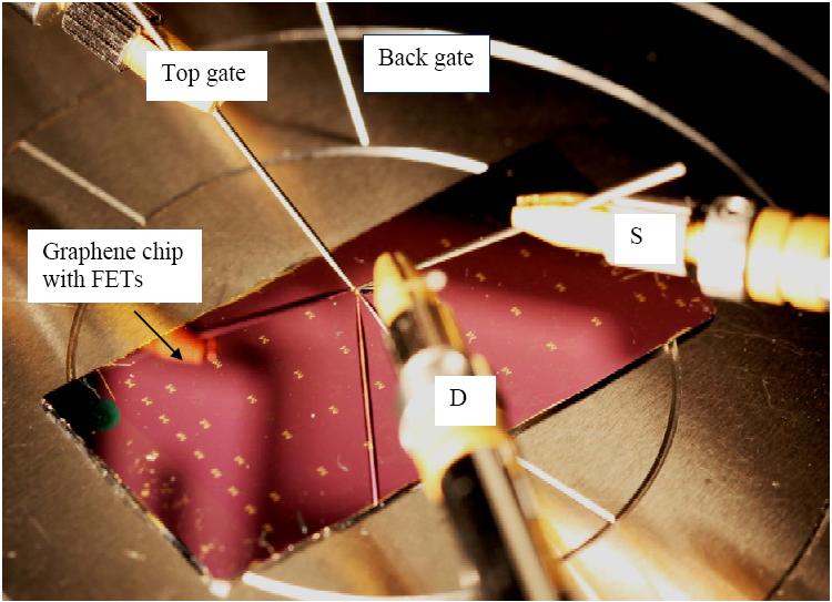
5 5 The graphene CVD transferred on the 4 inch Si/SiO 2 wafer displays two main distinct features: (i) about 70 % of the monolayer graphene area is practically defectless, (ii) 30 % of the graphene area contains defects (cracks, wrinkles, multilayer graphene). The Raman signature of the defectless graphene monolayer in Fig. 2(a) contains the G band at cm -1 and the 2D peak located at cm -1, the ratio between the 2D and G bands being about 2. No defect band D appears in this Raman signal. On the contrary, the Raman spectrum in Fig. 2(b), taken in a graphene area with defects, shows a peak associated to the D band, which indicates that the area under investigation is no longer an ideal graphene monolayer. In principle, it is a very tedious task to perform a Raman map of such a big chip, but a couple of Raman measurements must be done to locate the monolayer areas.the Raman spectra were obtained with a Labram Hr800 spectrometer and a laser excitation wavelength of 633 nm. All 60 graphene FETs fabricated on the graphene chip were measured in DC with the help of a Keithley 4200 SCS equipment with low noise amplifiers at its outputs. The DC probes connected to the Keithley 4200 were placed together with the probe station in a Faraday cage provided by Keithley. This system also allows the application of a back gate voltage up to 100 V via an interlock circuit. The graphene FET chip connected with the electrical probes for measurements is shown in Fig. 3. All measurements were done at room temperature with the source electrode connected to the ground. In the monolayer graphene regions we have seen NDR in all measured graphene FETs, whereas in the graphene area with defects the NDR behavior was not observed, the ballistic transport was lost, and the devices displayed FET-like I D -V D dependences that could be tuned by top and back gate voltages. From the 60 graphene FETs, 8 did not worked at all. As an example, a NDR with a tunable PVR depending on the top-gate voltage is represented in Fig. 4, where the I D -V D curves were measured at top gates of V TG = 0 V (red
6 6 dashed line), 0.5 V (blue dotted line) and 1 V (solid magenta line). The PVR ratio is enhanced by the gate voltage, as predicted in Ref. [11] in the case of a ballistic graphene FET with an oblique gate. The top gate voltage changes the Fermi level in graphene and thus modifies the shape of the NDR. For a top gate voltage of 1 V, the maximum drain current attains 105 A at a drain voltage of 1.5 V, and decreases to about 12 A at V D = 2 V. The PVR for this top gate voltage value is about On the contrary, when no gate voltage is applied the maximum and minimum I D values are about 95 A and 12 A, respectively, the corresponding PVR being 7.9. This NDR behavior was retrieved in many graphene FETs with oblique gates having PVRs in the 6-8 range, tunable by top gate voltages. The cutoff frequency of such a ballistic and tunable NDR device depends only on the transit time of carriers between drain and source. Thus, the cutoff frequency of the ballistic NDR in Fig. 1, with a drain-source distance of 400 nm and a Fermi velocity of 10 6 m/s, is in the THz range. However, the NDR behavior is lost in a non-ballistic transport regime. A typical I D -V D dependence in this case, shown in Fig. 5 for several top and gate voltages, looks different compared to a typical graphene FET. Unlike in the latter device, in which the I D -V D dependences are linear, in our graphene FETs they are clearly nonlinear. Because the graphene-cr/au contact is ohmic (Cr has the same workfunction as graphene monolayer, i.e. 4.5 ev), the nonlinearity can be attributed to the oblique gate. The various I D -V D curves in Fig. 5 correspond to: V TG = 2 V (green solid line), V TG = 1 V (magenta dotted line), V TG = 0 V(red dotted line), V TG = 1 V (blue dotted line), V TG = 2 V (solid blue line), V TG = 2 V and V BG = 40 V (solid magenta line), V TG = 2 V and V BG = 50 V (green dotted line), and V TG = 2 V and V BG = 60 V (solid red line). The different I D -V D characteristics in the graphene region with defects compared to those in defectless monolayer graphene can be explained by the fact that scattering on defects and impurities
7 7 randomize the propagation direction of charge carriers, changing also their energy if the scattering is inelastic. Because the position and width of the transmission gap that gives rise to NDR depends on the energy and propagation direction of charge carriers, it follows that the NDR disappears due to scattering-induced averaging, even if the phase of charge carrier wavefunction is preserved at scattering. From Fig. 5 it can be seen that the I D -V D characteristic is influenced by the top and gate voltages, the graphene FET being practically blocked for V TG = 2 V and V BG = 60 V, the corresponding characteristic being superimposed on the horizontal axis. At such a high back gate voltage the spatial charge of the very large number of charge carriers screens the applied source-drain voltage. Another effect of the non-ballistic transport regime is that the maxim drain current is now about 40 A i.e. it is reduced with more than 50% compared to the ballistic device in Fig. 4. Conclusions We have fabricated tens of graphene FETs having a tilted top gate on a CVD grown graphene monolayer chip. A large part of them, situated in the defect-free areas of the chip, are working in the ballistic regime and display NDR with a large PVR, having cutoff frequencies in the THz region. The other devices, situated in the area where defects are present, lose the NDR behavior, but display nonlinear I D -V D dependences tuned by top and back gate voltages. In the non-ballistic propagation regime, due to the scattering-induced lengthening of the charge carriers path in th device, the graphene FETs have a lower cutoff than those working in the ballistic regime, but could still be used in various RF applications.
8 8 References [1] X.Q. Deng, J.C. Zhou, Z. H. Zhang, H. Zhang, M. Qiu, Electrode conformation-induced negative differential resistance and rectifying performances in a molecular device, Appl. Phys. Lett. 95, (2009). [2] Y. Ya, J. Qui, W. Guo, Z. Qi, Y. Zhang, Electrical instability and negative differential resistance in single Sb-doped ZnO nanobelts/sio x /p-si heterostructure device, Appl. Phys. Lett. 96, (2010). [3] N.M. Park, S.H. Kim, S. Maeng, S.-J. Park, Negative differential resistance in silicon quantum dot metal-insulator semiconductor structure, Appl. Phys. Lett. 89, (2006). [4] M. Dragoman, G. Konstantinidis, A. Cismaru, D. Vasilache, A. Dinescu, D. Dragoman, D. Neculoiu, R. Buiculescu, G. Deligiorgis, A.P. Vajpeyi, A. Georgakilas, Negative differential resitance in GaN nanowire network, Appl. Phys. Lett. 96, (2010). [5] A. Radoi, M. Dragoman, A. Cismaru, G. Konstantinidis, D. Dragoman, Self-powered microwave devices based on graphene ink decorated with gold nanoislands, J. Appl. Phys. 112, (2012). [6] L. Britnell, R.V. Gorbachev, A.K. Geim, L.A. Ponomarenko, A. Mishchenko, M.T. Greenaway, T.M. Fromhold, K.S. Novoselov, L. Eaves, Resonant tunneling and negative differential conductance in graphene transistors, Nature Communications 4, 1794 (2013). [7] Y. Wu, D.B. Farmer, W. Zhu, S.-J. Han, C.D. Dimitripoulos, A.A. Bol, P. Avouris, Y.M. Lin, Three terminal graphene negative differential resistance devices, ACS Nano 4, (2012). [8] G. Liu, S. Ahsan, A.G. Khitun, R.K. Lake, A. Balandin, Graphene-based non-boolean logic circuits, J. Appl. Phys. 114, (2013).
9 9 [9] M. Dragoman, D. Dragoman, Nanoelectronics: Principles and Devices, 2 nd edition, Artech House, Boston (2009). [10] M.I. Katsnelson, K.S. Novoselov, A. K. Geim, Chiral tunnelling and the Klein paradox in graphene, Nature Physics 2, 620 (2006). [11] D. Dragoman, M. Dragoman, Negative differential resistance of electrons in graphene barrier, Appl. Phys. Lett. 90, (2007). [12] D. Dragoman, M. Dragoman, R. Plana, Graphene-based ultrafast diode, J. Appl. Phys. 108, (2010). [13] L. Liao, J. Bai, R. Cheng, Y.-C. Lin, S. Jiang, Y. Qu, Y. Huang, X. Duan, Sub-100 nm channel length graphene transistors, Nano Lett. 10, (2010). Acknowledgements We thank the European Commission for the financial support via the FP 7 NANO RF (grant agreement ). We also thank to eng. Adrian Albu for his help in the DC measurements of the graphene FET devices.
10 10 FIGURE CAPTIONS Fig. 1 SEM photo of the FET based on a graphene monolayer, with an oblique gate. Fig. 2 (a) Raman signature of the defectless graphene monolayer, and (b) Raman signature of the graphene region with defects. Fig. 3 The graphene FET chip under preparation to be measured on Keithley 4200 SCS. Fig. 4 NDR behavior in the ballistic regime of the graphene FET with oblique gate at V TG = 0 V (red dashed line), 0.5 V (blue dotted line) and 1 V (solid red line). Fig. 5 Drain current-drain voltage dependences of the graphene FET at various top and back gate voltages: V TG = 2 V (green solid line), V TG = 1 V (magenta dotted line), V TG = 0 V(red dotted line), V TG = 1 V (blue dotted line), V TG = 2 V (solid blue line), V TG = 2 V and V BG = 40 V (solid magenta line), V TG = 2 V and V BG = 50 V (green dotted line), and V TG = 2 V and V BG = 60 V (solid red line).
11 11 Oblique gate 40 nm D S 400 nm Graphene monolayer Fig. 1
12 12 (a. u.) Raman Shift (cm -1 ) (a) Intensity (a. u.) Raman shift (cm -1 ) (b) Fig. 2
13 Fig. 3 13
14 Fig. 4 14
15 Fig. 5 15
MICROWAVE AND MILLIMETERWAVE ELECTRICAL PERMITTIVITY OF GRAPHENE MONOLAYER. G. Konstantinidis 3
 1 MICROWAVE AND MILLIMETERWAVE ELECTRICAL PERMITTIVITY OF GRAPHENE MONOLAYER Alina Cismaru 1, Mircea Dragoman 1*, Adrian Dinescu 1, Daniela Dragoman 2, G. Stavrinidis, G. Konstantinidis 3 1 National Institute
Nanoscale Diodes Without p-n Junctions
 Nanoscale Diodes Without p-n Junctions Mircea DRAGOMAN National Institute for Research and Development in Microtechnology (IMT), P.O. Box 38-160, 023573 Bucharest, Romania E-mail: mircea.dragoman@imt.ro
ROOM TEMPERATURE ON-WAFER BALLISTIC GRAPHENE FIELD- EFFECT-TRANSISTOR WITH OBLIQUE DOUBLE-GATE , Bucharest, Romania, Romania
 1 ROOM TEMPERATURE ON-WAFER BALLISTIC GRAPHENE FIELD- EFFECT-TRANSISTOR WITH OBLIQUE DOUBLE-GATE Mircea Dragoman 1*, Adrian Dinescu 1, and Daniela Dragoman 2,3 1 National Institute for Research and Development
Graphene A One-Atom-Thick Material for Microwave Devices
 ROMANIAN JOURNAL OF INFORMATION SCIENCE AND TECHNOLOGY Volume 11, Number 1, 2008, 29 35 Graphene A One-Atom-Thick Material for Microwave Devices D. DRAGOMAN 1, M. DRAGOMAN 2, A. A. MÜLLER3 1 University
Beyond silicon electronics-fets with nanostructured graphene channels with high on-off ratio and highmobility
 Beyond silicon electronics-fets with nanostructured graphene channels with high on-off ratio and highmobility M.Dragoman 1, A.Dinescu 1, and D.Dragoman 2 1 National Institute for Research and Development
Ph.D. students, postdocs, and young researchers, which need to absorb a lot of new knowledge, not taught at universities, in a rather short time.
 We have started to work in the area of graphene at the end of 2006, discovering that the fascinating Dirac equations could drive to new discoveries in solid-state physics. At that time, although the Dirac
Nanoscale diodes without p-n junctions. Mircea Dragoman IMT Bucharest
 Nanoscale diodes without p-n junctions. Mircea Dragoman IMT Bucharest Coplanar electrodes on graphene-graphene radio Dissimilar electrodes Schottky diode Geometric diodesgraphene on wafer Schottky contact
Multicolor Graphene Nanoribbon/Semiconductor Nanowire. Heterojunction Light-Emitting Diodes
 Multicolor Graphene Nanoribbon/Semiconductor Nanowire Heterojunction Light-Emitting Diodes Yu Ye, a Lin Gan, b Lun Dai, *a Hu Meng, a Feng Wei, a Yu Dai, a Zujin Shi, b Bin Yu, a Xuefeng Guo, b and Guogang
Supporting Online Material for
 www.sciencemag.org/cgi/content/full/327/5966/662/dc Supporting Online Material for 00-GHz Transistors from Wafer-Scale Epitaxial Graphene Y.-M. Lin,* C. Dimitrakopoulos, K. A. Jenkins, D. B. Farmer, H.-Y.
ROOM TEMPERATURE NANOSTRUCTURED GRAPHENE TRANSISTOR WITH HIGH ON/OFF RATIO Bucharest, Romania,
 1 ROOM TEMPERATURE NANOSTRUCTURE GRAPHENE TRANSISTOR WITH HIGH ON/OFF RATIO Mircea ragoman 1*, Adrian inescu 1, and aniela ragoman 2,3 1 National Institute for Research and evelopment in Microtechnology
SUPPLEMENTARY INFORMATION
 doi:.38/nature09979 I. Graphene material growth and transistor fabrication Top-gated graphene RF transistors were fabricated based on chemical vapor deposition (CVD) grown graphene on copper (Cu). Cu foil
Impact of intrinsic deformations on the negative differential resistance of monolayer MoS 2 ultrashort channel MOSFET
 Impact of intrinsic deformations on the negative differential resistance of monolayer MoS 2 ultrashort channel MOSFET Amretashis Sengupta*, Santanu Mahapatra Nano-Scale Device Research Laboratory, Dept.
(a) (b) Supplementary Figure 1. (a) (b) (a) Supplementary Figure 2. (a) (b) (c) (d) (e)
 (b) Supplementary Figure 1. (a) (b) (a) Supplementary Figure 2. (a) (b) (c) (d) (e)") (a) (b) Supplementary Figure 1. (a) An AFM image of the device after the formation of the contact electrodes and the top gate dielectric Al 2 O 3. (b) A line scan performed along the white dashed line
(a) (b) Supplementary Figure 1. (a) An AFM image of the device after the formation of the contact electrodes and the top gate dielectric Al 2 O 3. (b) A line scan performed along the white dashed line
ELECTRONIC DEVICES BASED ON CARBON NANOTUBES AND GRAPHENE
 THE PUBLISHING HOUSE PROCEEDINGS OF THE ROMANIAN ACADEMY, Series A, OF THE ROMANIAN ACADEMY Volume 10, Number 1/2009, pp. 000 000 ELECTRONIC DEVICES BASED ON CARBON NANOTUBES AND GRAPHENE Mircea DRAGOMAN
Supporting Information. by Hexagonal Boron Nitride
 Supporting Information High Velocity Saturation in Graphene Encapsulated by Hexagonal Boron Nitride Megan A. Yamoah 1,2,, Wenmin Yang 1,3, Eric Pop 4,5,6, David Goldhaber-Gordon 1 * 1 Department of Physics,
TWO- AND THREE-QUBIT ROOM-TEMPERATURE GRAPHENE QUANTUM GATES. Daniela Dragoman 1 and Mircea Dragoman Bucharest, Romania
 1 TWO- AND THREE-QUBIT ROOM-TEMPERATURE GRAPHENE QUANTUM GATES Daniela Dragoman 1 and Mircea Dragoman 2 1 Univ. Bucharest, Faculty of Physics, P.O. Box MG-11, 077125 Bucharest, Romania 2 National Institute
Black phosphorus: A new bandgap tuning knob
 Black phosphorus: A new bandgap tuning knob Rafael Roldán and Andres Castellanos-Gomez Modern electronics rely on devices whose functionality can be adjusted by the end-user with an external knob. A new
Quantum Phenomena & Nanotechnology (4B5)
") Quantum Phenomena & Nanotechnology (4B5) The 2-dimensional electron gas (2DEG), Resonant Tunneling diodes, Hot electron transistors Lecture 11 In this lecture, we are going to look at 2-dimensional electron
Quantum Phenomena & Nanotechnology (4B5) The 2-dimensional electron gas (2DEG), Resonant Tunneling diodes, Hot electron transistors Lecture 11 In this lecture, we are going to look at 2-dimensional electron
Operating Principles of Vertical Transistors Based on Monolayer Two-Dimensional Semiconductor Heterojunctions
 Operating Principles of Vertical Transistors Based on Monolayer Two-Dimensional Semiconductor Heterojunctions Kai Tak Lam, Gyungseon Seol and Jing Guo Department of Electrical and Computer Engineering,
Tunneling characteristics of graphene
 Tunneling characteristics of graphene Young Jun Shin, 1,2 Gopinadhan Kalon, 1,2 Jaesung Son, 1 Jae Hyun Kwon, 1,2 Jing Niu, 1 Charanjit S. Bhatia, 1 Gengchiau Liang, 1 and Hyunsoo Yang 1,2,a) 1 Department
Graphene photodetectors with ultra-broadband and high responsivity at room temperature
 SUPPLEMENTARY INFORMATION DOI: 10.1038/NNANO.2014.31 Graphene photodetectors with ultra-broadband and high responsivity at room temperature Chang-Hua Liu 1, You-Chia Chang 2, Ted Norris 1.2* and Zhaohui
Formation of unintentional dots in small Si nanostructures
 Superlattices and Microstructures, Vol. 28, No. 5/6, 2000 doi:10.1006/spmi.2000.0942 Available online at http://www.idealibrary.com on Formation of unintentional dots in small Si nanostructures L. P. ROKHINSON,
GHZ ELECTRICAL PROPERTIES OF CARBON NANOTUBES ON SILICON DIOXIDE MICRO BRIDGES
 GHZ ELECTRICAL PROPERTIES OF CARBON NANOTUBES ON SILICON DIOXIDE MICRO BRIDGES SHENG F. YEN 1, HAROON LAIS 1, ZHEN YU 1, SHENGDONG LI 1, WILLIAM C. TANG 1,2, AND PETER J. BURKE 1,2 1 Electrical Engineering
Electric Field-Dependent Charge-Carrier Velocity in Semiconducting Carbon. Nanotubes. Yung-Fu Chen and M. S. Fuhrer
 Electric Field-Dependent Charge-Carrier Velocity in Semiconducting Carbon Nanotubes Yung-Fu Chen and M. S. Fuhrer Department of Physics and Center for Superconductivity Research, University of Maryland,
From nanophysics research labs to cell phones. Dr. András Halbritter Department of Physics associate professor
 From nanophysics research labs to cell phones Dr. András Halbritter Department of Physics associate professor Curriculum Vitae Birth: 1976. High-school graduation: 1994. Master degree: 1999. PhD: 2003.
NiCl2 Solution concentration. Etching Duration. Aspect ratio. Experiment Atmosphere Temperature. Length(µm) Width (nm) Ar:H2=9:1, 150Pa
 Width (nm) Ar:H2=9:1, 150Pa") Experiment Atmosphere Temperature #1 # 2 # 3 # 4 # 5 # 6 # 7 # 8 # 9 # 10 Ar:H2=9:1, 150Pa Ar:H2=9:1, 150Pa Ar:H2=9:1, 150Pa Ar:H2=9:1, 150Pa Ar:H2=9:1, 150Pa Ar:H2=9:1, 150Pa Ar:H2=9:1, 150Pa Ar:H2=9:1,
Experiment Atmosphere Temperature #1 # 2 # 3 # 4 # 5 # 6 # 7 # 8 # 9 # 10 Ar:H2=9:1, 150Pa Ar:H2=9:1, 150Pa Ar:H2=9:1, 150Pa Ar:H2=9:1, 150Pa Ar:H2=9:1, 150Pa Ar:H2=9:1, 150Pa Ar:H2=9:1, 150Pa Ar:H2=9:1,
Supporting Online Material for
 www.sciencemag.org/cgi/content/full/320/5874/356/dc1 Supporting Online Material for Chaotic Dirac Billiard in Graphene Quantum Dots L. A. Ponomarenko, F. Schedin, M. I. Katsnelson, R. Yang, E. W. Hill,
SUPPLEMENTARY INFORMATION
 SUPPLEMENTARY INFORMATION DOI: 10.1038/NNANO.2011.138 Graphene Nanoribbons with Smooth Edges as Quantum Wires Xinran Wang, Yijian Ouyang, Liying Jiao, Hailiang Wang, Liming Xie, Justin Wu, Jing Guo, and
Graphene Field Effect Devices Operating in Differential Circuit Configuration
 Graphene Field Effect Devices Operating in Differential Circuit Configuration C. Nyffeler a,*, M.S. Hanay b,c, D. Sacchetto a, Y. Leblebici a a Institute of Electrical Engineering, EPFL, Lausanne, Switzerland
A. Optimizing the growth conditions of large-scale graphene films
 1 A. Optimizing the growth conditions of large-scale graphene films Figure S1. Optical microscope images of graphene films transferred on 300 nm SiO 2 /Si substrates. a, Images of the graphene films grown
SUPPLEMENTARY INFORMATION. Observation of tunable electrical bandgap in large-area twisted bilayer graphene synthesized by chemical vapor deposition
 SUPPLEMENTARY INFORMATION Observation of tunable electrical bandgap in large-area twisted bilayer graphene synthesized by chemical vapor deposition Jing-Bo Liu 1 *, Ping-Jian Li 1 *, Yuan-Fu Chen 1, Ze-Gao
SUPPLEMENTARY INFORMATION
 doi:10.1038/nature11231 Materials and Methods: Sample fabrication: Highly oriented VO 2 thin films on Al 2 O 3 (0001) substrates were deposited by reactive sputtering from a vanadium target through reactive
IS THERE ANY KLEIN PARADOX? LOOK AT GRAPHENE! D. Dragoman Univ. Bucharest, Physics Dept., P.O. Box MG-11, Bucharest,
 1 IS THERE ANY KLEIN PARADOX? LOOK AT GRAPHENE! D. Dragoman Univ. Bucharest, Physics Dept., P.O. Box MG-11, 077125 Bucharest, Romania, e-mail: danieladragoman@yahoo.com Abstract It is demonstrated that
Title: Ultrafast photocurrent measurement of the escape time of electrons and holes from
 Title: Ultrafast photocurrent measurement of the escape time of electrons and holes from carbon nanotube PN junction photodiodes Authors: Nathaniel. M. Gabor 1,*, Zhaohui Zhong 2, Ken Bosnick 3, Paul L.
Wafer-Scale Single-Domain-Like Graphene by. Defect-Selective Atomic Layer Deposition of
 Electronic Supplementary Material (ESI) for Nanoscale. This journal is The Royal Society of Chemistry 2015 Wafer-Scale Single-Domain-Like Graphene by Defect-Selective Atomic Layer Deposition of Hexagonal
Supplementary Figure S1. AFM images of GraNRs grown with standard growth process. Each of these pictures show GraNRs prepared independently,
 Supplementary Figure S1. AFM images of GraNRs grown with standard growth process. Each of these pictures show GraNRs prepared independently, suggesting that the results is reproducible. Supplementary Figure
Transport through Andreev Bound States in a Superconductor-Quantum Dot-Graphene System
 Transport through Andreev Bound States in a Superconductor-Quantum Dot-Graphene System Nadya Mason Travis Dirk, Yung-Fu Chen, Cesar Chialvo Taylor Hughes, Siddhartha Lal, Bruno Uchoa Paul Goldbart University
Transport Properties of Graphene Nanoribbon Transistors on. Chemical-Vapor-Deposition Grown Wafer-Scale Graphene
 Transport Properties of Graphene Nanoribbon Transistors on Chemical-Vapor-Deposition Grown Wafer-Scale Graphene Wan Sik Hwang 1, a), Kristof Tahy 1, Xuesong Li 2, Huili (Grace) Xing 1, Alan C. Seabaugh
Session Chair: Prof. Haiping Cheng (University of Florida) Dr. Lei Shen. National University of Singapore
 Dr. Lei Shen. National University of Singapore") B1. Modeling Quantum Transport at Nanoscale Chair(s): Chun ZHANG, National University of Singapore, Singapore Session s Title (if available) Tue - 17 Jan 2017 13:00 ~ 14:30 Room 2 Session Chair: Prof.
B1. Modeling Quantum Transport at Nanoscale Chair(s): Chun ZHANG, National University of Singapore, Singapore Session s Title (if available) Tue - 17 Jan 2017 13:00 ~ 14:30 Room 2 Session Chair: Prof.
Explicit drain current, charge and capacitance model of graphene field-effect transistors. David Jiménez
 Explicit drain current, charge and capacitance model of graphene field-effect transistors David Jiménez Departament d'enginyeria Electrònica, Escola d'enginyeria, Universitat Autònoma de Barcelona, 08193-Bellaterra,
Supplementary Figure 1. Supplementary Figure 1 Characterization of another locally gated PN junction based on boron
 Supplementary Figure 1 Supplementary Figure 1 Characterization of another locally gated PN junction based on boron nitride and few-layer black phosphorus (device S1). (a) Optical micrograph of device S1.
Nanocarbon Technology for Development of Innovative Devices
 Nanocarbon Technology for Development of Innovative Devices Shintaro Sato Daiyu Kondo Shinichi Hirose Junichi Yamaguchi Graphene, a one-atom-thick honeycomb lattice made of carbon, and a carbon nanotube,
M R S Internet Journal of Nitride Semiconductor Research
 Page 1 of 6 M R S Internet Journal of Nitride Semiconductor Research Volume 9, Article 7 The Ambient Temperature Effect on Current-Voltage Characteristics of Surface-Passivated GaN-Based Field-Effect Transistors
A Bottom-gate Depletion-mode Nanowire Field Effect Transistor (NWFET) Model Including a Schottky Diode Model
 Model Including a Schottky Diode Model") Journal of the Korean Physical Society, Vol. 55, No. 3, September 2009, pp. 1162 1166 A Bottom-gate Depletion-mode Nanowire Field Effect Transistor (NWFET) Model Including a Schottky Diode Model Y. S.
Journal of the Korean Physical Society, Vol. 55, No. 3, September 2009, pp. 1162 1166 A Bottom-gate Depletion-mode Nanowire Field Effect Transistor (NWFET) Model Including a Schottky Diode Model Y. S.
1. Nanotechnology & nanomaterials -- Functional nanomaterials enabled by nanotechnologies.
 Novel Nano-Engineered Semiconductors for Possible Photon Sources and Detectors NAI-CHANG YEH Department of Physics, California Institute of Technology 1. Nanotechnology & nanomaterials -- Functional nanomaterials
Normally-Off GaN Field Effect Power Transistors: Device Design and Process Technology Development
 Center for High Performance Power Electronics Normally-Off GaN Field Effect Power Transistors: Device Design and Process Technology Development Dr. Wu Lu (614-292-3462, lu.173@osu.edu) Dr. Siddharth Rajan
Supplementary Figure 1 Dark-field optical images of as prepared PMMA-assisted transferred CVD graphene films on silicon substrates (a) and the one
 and the one") Supplementary Figure 1 Dark-field optical images of as prepared PMMA-assisted transferred CVD graphene films on silicon substrates (a) and the one after PBASE monolayer growth (b). 1 Supplementary Figure
Supplementary Figure 1 Dark-field optical images of as prepared PMMA-assisted transferred CVD graphene films on silicon substrates (a) and the one after PBASE monolayer growth (b). 1 Supplementary Figure
Extrinsic Origin of Persistent Photoconductivity in
 Supporting Information Extrinsic Origin of Persistent Photoconductivity in Monolayer MoS2 Field Effect Transistors Yueh-Chun Wu 1, Cheng-Hua Liu 1,2, Shao-Yu Chen 1, Fu-Yu Shih 1,2, Po-Hsun Ho 3, Chun-Wei
Giant Gating Tunability of Optical Refractive Index in Transition Metal Dichalcogenide Monolayers
 Supporting Information Giant Gating Tunability of Optical Refractive Index in Transition Metal Dichalcogenide Monolayers Yiling Yu 1,2, Yifei Yu 1, Lujun Huang 1, Haowei Peng 3, Liwei Xiong 1,4 and Linyou
Terahertz sensing and imaging based on carbon nanotubes:
 Terahertz sensing and imaging based on carbon nanotubes: Frequency-selective detection and near-field imaging Yukio Kawano RIKEN, JST PRESTO ykawano@riken.jp http://www.riken.jp/lab-www/adv_device/kawano/index.html
Monolayer Semiconductors
 Monolayer Semiconductors Gilbert Arias California State University San Bernardino University of Washington INT REU, 2013 Advisor: Xiaodong Xu (Dated: August 24, 2013) Abstract Silicon may be unable to
Supplementary Methods A. Sample fabrication
 Supplementary Methods A. Sample fabrication Supplementary Figure 1(a) shows the SEM photograph of a typical sample, with three suspended graphene resonators in an array. The cross-section schematic is
GaN based transistors
 GaN based transistors S FP FP dielectric G SiO 2 Al x Ga 1-x N barrier i-gan Buffer i-sic D Transistors "The Transistor was probably the most important invention of the 20th Century The American Institute
Theoretical Study on Graphene Silicon Heterojunction Solar Cell
 Copyright 2015 American Scientific Publishers All rights reserved Printed in the United States of America Journal of Nanoelectronics and Optoelectronics Vol. 10, 1 5, 2015 Theoretical Study on Graphene
2D MBE Activities in Sheffield. I. Farrer, J. Heffernan Electronic and Electrical Engineering The University of Sheffield
 2D MBE Activities in Sheffield I. Farrer, J. Heffernan Electronic and Electrical Engineering The University of Sheffield Outline Motivation Van der Waals crystals The Transition Metal Di-Chalcogenides
Hopping in CVD Grown Single-layer MoS 2
 Supporting Information for Large Thermoelectricity via Variable Range Hopping in CVD Grown Single-layer MoS 2 Jing Wu 1,2,3, Hennrik Schmidt 1,2, Kiran Kumar Amara 4, Xiangfan Xu 5, Goki Eda 1,2,4, and
Impact of disorder and topology in two dimensional systems at low carrier densities
 Impact of disorder and topology in two dimensional systems at low carrier densities A Thesis Submitted For the Degree of Doctor of Philosophy in the Faculty of Science by Mohammed Ali Aamir Department
Chapter 3 The InAs-Based nbn Photodetector and Dark Current
 68 Chapter 3 The InAs-Based nbn Photodetector and Dark Current The InAs-based nbn photodetector, which possesses a design that suppresses surface leakage current, is compared with both a commercially available
Supporting Information Available:
 Supporting Information Available: Photoresponsive and Gas Sensing Field-Effect Transistors based on Multilayer WS 2 Nanoflakes Nengjie Huo 1, Shengxue Yang 1, Zhongming Wei 2, Shu-Shen Li 1, Jian-Bai Xia
THz operation of self-switching nano-diodes and nano-transistors
 THz operation of self-switching nano-diodes and nano-transistors J. Mateos 1, A.M. Song 2, B.G. Vasallo 1, D. Pardo 1, and T. González 1 1 Departamento de Física Aplicada, Universidad de Salamanca, Salamanca,
Nanoelectronics. Topics
 Nanoelectronics Topics Moore s Law Inorganic nanoelectronic devices Resonant tunneling Quantum dots Single electron transistors Motivation for molecular electronics The review article Overview of Nanoelectronic
Suppression of 1/f Noise in Near-Ballistic h-bn-graphene-h-bn Heterostructure Field-Effect Transistors
 Suppression of 1/f Noise in Near-Ballistic h-bn-graphene-h-bn Heterostructure Field-Effect Transistors Maxim A. Stolyarov 1, Guanxiong Liu 1, Sergey L. Rumyantsev 2,3, Michael Shur 2 and Alexander A. Balandin
Graphene for Microwaves
 T hese days, electronics are moving toward faster, smaller, more efficient, yet cost effective, solutions. In doing so, the limits of what materials are currently available within the technologies are
Intrinsic Electronic Transport Properties of High. Information
 Intrinsic Electronic Transport Properties of High Quality and MoS 2 : Supporting Information Britton W. H. Baugher, Hugh O. H. Churchill, Yafang Yang, and Pablo Jarillo-Herrero Department of Physics, Massachusetts
DETECTION OF ELECTROMAGNETIC WAVES WITH A SINGLE CARBON ATOM SHEET
 THE PUBLISHING HOUSE PROCEEDINGS OF THE ROMANIAN ACADEMY, Series A, OF THE ROMANIAN ACADEMY Volume 15, Number 2/2014, pp. 208 215 DETECTION OF ELECTROMAGNETIC WAVES WITH A SINGLE CARBON ATOM SHEET Mircea
SUPPLEMENTARY INFORMATION
 SUPPLEMENTARY INFORMATION Flexible, high-performance carbon nanotube integrated circuits Dong-ming Sun, Marina Y. Timmermans, Ying Tian, Albert G. Nasibulin, Esko I. Kauppinen, Shigeru Kishimoto, Takashi
Graphene and Carbon Nanotubes
 Graphene and Carbon Nanotubes 1 atom thick films of graphite atomic chicken wire Novoselov et al - Science 306, 666 (004) 100μm Geim s group at Manchester Novoselov et al - Nature 438, 197 (005) Kim-Stormer
Large Scale Direct Synthesis of Graphene on Sapphire and Transfer-free Device Fabrication
 Supplementary Information Large Scale Direct Synthesis of Graphene on Sapphire and Transfer-free Device Fabrication Hyun Jae Song a, Minhyeok Son a, Chibeom Park a, Hyunseob Lim a, Mark P. Levendorf b,
Fermi Level Pinning at Electrical Metal Contacts. of Monolayer Molybdenum Dichalcogenides
 Supporting information Fermi Level Pinning at Electrical Metal Contacts of Monolayer Molybdenum Dichalcogenides Changsik Kim 1,, Inyong Moon 1,, Daeyeong Lee 1, Min Sup Choi 1, Faisal Ahmed 1,2, Seunggeol
vapour deposition. Raman peaks of the monolayer sample grown by chemical vapour
 Supplementary Figure 1 Raman spectrum of monolayer MoS 2 grown by chemical vapour deposition. Raman peaks of the monolayer sample grown by chemical vapour deposition (S-CVD) are peak which is at 385 cm
Carbon Nanotube Devices for GHz to THz Applications
 Invited Paper Carbon Nanotube Devices for GHz to THz Applications Peter J. Burke * Department of Electrical Engineering and Computer Science University of California, Irvine Irvine, CA 92697-2625 ABSTRACT
Chapter 3 Properties of Nanostructures
 Chapter 3 Properties of Nanostructures In Chapter 2, the reduction of the extent of a solid in one or more dimensions was shown to lead to a dramatic alteration of the overall behavior of the solids. Generally,
Current mechanisms Exam January 27, 2012
 Current mechanisms Exam January 27, 2012 There are four mechanisms that typically cause currents to flow: thermionic emission, diffusion, drift, and tunneling. Explain briefly which kind of current mechanisms
smal band gap Saturday, April 9, 2011
 small band gap upper (conduction) band empty small gap valence band filled 2s 2p 2s 2p hybrid (s+p)band 2p no gap 2s (depend on the crystallographic orientation) extrinsic semiconductor semi-metal electron
Diameter Optimization for Highest Degree of Ballisticity of Carbon Nanotube Field Effect Transistors I. Khan, O. Morshed and S. M.
 Diameter Optimization for Highest Degree of Ballisticity of Carbon Nanotube Field Effect Transistors I. Khan, O. Morshed and S. M. Mominuzzaman Department of Electrical and Electronic Engineering, Bangladesh
Figure 1: Graphene release, transfer and stacking processes. The graphene stacking began with CVD
 Supplementary figure 1 Graphene Growth and Transfer Graphene PMMA FeCl 3 DI water Copper foil CVD growth Back side etch PMMA coating Copper etch in 0.25M FeCl 3 DI water rinse 1 st transfer DI water 1:10
Spatially resolving density-dependent screening around a single charged atom in graphene
 Supplementary Information for Spatially resolving density-dependent screening around a single charged atom in graphene Dillon Wong, Fabiano Corsetti, Yang Wang, Victor W. Brar, Hsin-Zon Tsai, Qiong Wu,
Supplementary Materials for
 advances.sciencemag.org/cgi/content/full/2/9/e1601240/dc1 Supplementary Materials for Quasi-ballistic carbon nanotube array transistors with current density exceeding Si and GaAs Gerald J. Brady, Austin
Evaluation of Electronic Characteristics of Double Gate Graphene Nanoribbon Field Effect Transistor for Wide Range of Temperatures
 Evaluation of Electronic Characteristics of Double Gate Graphene Nanoribbon Field Effect Transistor for Wide Range of Temperatures 1 Milad Abtin, 2 Ali Naderi 1 Department of electrical engineering, Masjed
Transport properties through double-magnetic-barrier structures in graphene
 Chin. Phys. B Vol. 20, No. 7 (20) 077305 Transport properties through double-magnetic-barrier structures in graphene Wang Su-Xin( ) a)b), Li Zhi-Wen( ) a)b), Liu Jian-Jun( ) c), and Li Yu-Xian( ) c) a)
Supplementary information for Tunneling Spectroscopy of Graphene-Boron Nitride Heterostructures
 Supplementary information for Tunneling Spectroscopy of Graphene-Boron Nitride Heterostructures F. Amet, 1 J. R. Williams, 2 A. G. F. Garcia, 2 M. Yankowitz, 2 K.Watanabe, 3 T.Taniguchi, 3 and D. Goldhaber-Gordon
Electronic Supplementary Information for
 Electronic Supplementary Material (ESI) for Journal of Materials Chemistry C. This journal is The Royal Society of Chemistry 018 Electronic Supplementary Information for Broadband Photoresponse Based on
Tunneling transport. Courtesy Prof. S. Sawyer, RPI Also Davies Ch. 5
 unneling transport Courtesy Prof. S. Sawyer, RPI Also Davies Ch. 5 Electron transport properties l e : electronic mean free path l φ : phase coherence length λ F : Fermi wavelength ecture Outline Important
Supplementary Information for
 Supplementary Information for Highly Stable, Dual-Gated MoS 2 Transistors Encapsulated by Hexagonal Boron Nitride with Gate-Controllable Contact Resistance and Threshold Voltage Gwan-Hyoung Lee, Xu Cui,
Contact Engineering of Two-Dimensional Layered Semiconductors beyond Graphene
 Contact Engineering of Two-Dimensional Layered Semiconductors beyond Graphene Zhixian Zhou Department of Physics and Astronomy Wayne State University Detroit, Michigan Outline Introduction Ionic liquid
Detection of Ionizing Radiations with Graphene Field Effect Transistors (GFET) Yong P. Chen Purdue University
 Yong P. Chen Purdue University") Detection of Ionizing Radiations with Graphene Field Effect Transistors (GFET) Yong P. Chen (yongchen@purdue.edu), Purdue University IEEE NSS 10/26/2009 Team Members: Isaac Childres, Mike Foxe, Gabriel
Detection of Ionizing Radiations with Graphene Field Effect Transistors (GFET) Yong P. Chen (yongchen@purdue.edu), Purdue University IEEE NSS 10/26/2009 Team Members: Isaac Childres, Mike Foxe, Gabriel
The effect of light illumination in photoionization of deep traps in GaN MESFETs buffer layer using an ensemble Monte Carlo simulation
 International Journal of Physical Sciences Vol. 6(2), pp. 273-279, 18 January, 2011 Available online at http://www.academicjournals.org/ijps ISSN 1992-1950 2011 Academic Journals Full Length Research Paper
Carbon based Nanoscale Electronics
 Carbon based Nanoscale Electronics 09 02 200802 2008 ME class Outline driving force for the carbon nanomaterial electronic properties of fullerene exploration of electronic carbon nanotube gold rush of
Drift-diffusion model for single layer transition metal dichalcogenide field-effect transistors
 Drift-diffusion model for single layer transition metal dichalcogenide field-effect transistors David Jiménez Departament d'enginyeria Electrònica, Escola d'enginyeria, Universitat Autònoma de Barcelona,
SUPPLEMENTARY INFORMATION
 Supplementary Information: Photocurrent generation in semiconducting and metallic carbon nanotubes Maria Barkelid 1*, Val Zwiller 1 1 Kavli Institute of Nanoscience, Delft University of Technology, Delft,
TRANSVERSE SPIN TRANSPORT IN GRAPHENE
 International Journal of Modern Physics B Vol. 23, Nos. 12 & 13 (2009) 2641 2646 World Scientific Publishing Company TRANSVERSE SPIN TRANSPORT IN GRAPHENE TARIQ M. G. MOHIUDDIN, A. A. ZHUKOV, D. C. ELIAS,
Planar Organic Photovoltaic Device. Saiful I. Khondaker
 Planar Organic Photovoltaic Device Saiful I. Khondaker Nanoscience Technology Center and Department of Physics University of Central Florida http://www.physics.ucf.edu/~khondaker W Metal 1 L ch Metal 2
Electrostatics of Nanowire Transistors
 Electrostatics of Nanowire Transistors Jing Guo, Jing Wang, Eric Polizzi, Supriyo Datta and Mark Lundstrom School of Electrical and Computer Engineering Purdue University, West Lafayette, IN, 47907 ABSTRACTS
Supplementary Figure 1. Selected area electron diffraction (SAED) of bilayer graphene and tblg. (a) AB
 of bilayer graphene and tblg. (a) AB") Supplementary Figure 1. Selected area electron diffraction (SAED) of bilayer graphene and tblg. (a) AB stacked bilayer graphene (b), (c), (d), (e), and (f) are twisted bilayer graphene with twist angle
Supplementary Figure 1. Selected area electron diffraction (SAED) of bilayer graphene and tblg. (a) AB stacked bilayer graphene (b), (c), (d), (e), and (f) are twisted bilayer graphene with twist angle
Raman spectroscopy at the edges of multilayer graphene
 Raman spectroscopy at the edges of multilayer graphene Q. -Q. Li, X. Zhang, W. -P. Han, Y. Lu, W. Shi, J. -B. Wu, P. -H. Tan* State Key Laboratory of Superlattices and Microstructures, Institute of Semiconductors,
single-electron electron tunneling (SET)
") single-electron electron tunneling (SET) classical dots (SET islands): level spacing is NOT important; only the charging energy (=classical effect, many electrons on the island) quantum dots: : level spacing
single-electron electron tunneling (SET) classical dots (SET islands): level spacing is NOT important; only the charging energy (=classical effect, many electrons on the island) quantum dots: : level spacing
Supporting Information
 Electronic Supplementary Material (ESI) for ChemComm. This journal is The Royal Society of Chemistry 2014 Supporting Information Controllable Atmospheric Pressure Growth of Mono-layer, Bi-layer and Tri-layer
A Graphene-based Hot Electron Transistor
 This work has been published in Nano Letters (ACS Publications) Nano Lett., 2013, 13 (4), pp 1435 1439 DOI: 10.1021/nl304305x A Graphene-based Hot Electron Transistor Sam Vaziri 1,#, Grzegorz Lupina 2,#,
NANOELECTRONICS ON A SINGLE ATOM SHEET
 Romanian Reports in Physics, Vol. 65, No. 3, P. 792 804, 2013 Dedicated to Professor Valentin I. Vlad s 70 th Anniversary NANOELECTRONICS ON A SINGLE ATOM SHEET MIRCEA DRAGOMAN National Institute for Research
Raman Imaging and Electronic Properties of Graphene
 Raman Imaging and Electronic Properties of Graphene F. Molitor, D. Graf, C. Stampfer, T. Ihn, and K. Ensslin Laboratory for Solid State Physics, ETH Zurich, 8093 Zurich, Switzerland ensslin@phys.ethz.ch