Nanoscale diodes without p-n junctions. Mircea Dragoman IMT Bucharest
|
|
|
- Geraldine Grant
- 5 years ago
- Views:
Transcription


 (100 nm width)")
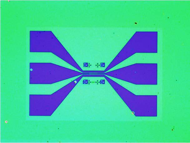
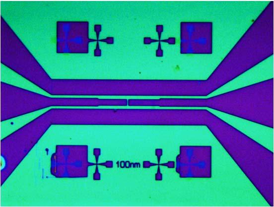
1 Nanoscale diodes without p-n junctions. Mircea Dragoman IMT Bucharest Coplanar electrodes on graphene-graphene radio Dissimilar electrodes Schottky diode Geometric diodesgraphene on wafer Schottky contact (Ti) (100 nm width) Ohmic contact-pt graphene


2 Carbon-based materials K.S. Novoselov et al., Science 306 (2004) 666 Theory: P.R. Wallace, Phys. Rev. 71 (1947) 622 S. Iijima, Nature 354 (1991) 56 H.W. Kroto et al., Nature 318 (1985) 162


 250 L.D.")


3 Graphene: Should it exist? Two-dimensional crystals are thermodinamically unstable! R.E. Peierls, Ann. I.H. Poincare 5 (1935) 177 N.D. Mermin, Phys. Rev. 176 (1968) 250 L.D. Landau, E.M. Lifshitz, Statistical Physics, Pergamon (1980) thickness < 20 nm However.. HOPG G. Reiter, Langmuir 9 (1993) 1344 rub deposit on 300 μm SiO 2 A.K. Geim, P. Kim, Sci. Am., April 2008, 90 thickness 0.34 nm


4 Why the current is flowing in graphene? Isolated atom orbitals σ-electrons p orbitals sp 2 orbitals sp 2 carbon sp 2 carbon Molecule-hybridization of orbitals; localized electrons Current flow pi orbitals π-electrons not hybridized, are not localized Carbon-carbon double bond n αv g K.S. Novoselov et al., Science 315 (2007) 1379
 How we can identify graphene? Z.H. Ni et. al.")
 Raman signature Number of layers A.C.")
5 Optical view of different graphene layers (mono, bi and multilayers) How we can identify graphene? Z.H. Ni et. al., Nano Lett., pp (2007) Raman signature Number of layers A.C. Ferrari et. al., Pyhs. Rev. Lett. 97, (2006)


6 Band structure E± ( k) = ± vf k v F c / 300 E m = = 0, m 2 c c D.L. Miller et al., Science 324 (2009) = + v F p 2 c 2 S.Y.Zhou et al., Nature Physics 2 (2006) 595
 maximum mobility : 200 000 cm 2 V 1 s 1 ) on suspended graphene or")
7 Parameter Value and units Observations Thermal conductivity 5000 W/mK Better thermal conductivity than in most crystals Young modulus 1.5 TPa Ten times greater than in steel bilayer monolayer Mobility cm 2 V 1 s 1 At room temperature (intrinsic mobility) maximum mobility : cm 2 V 1 s 1 ) on suspended graphene or graphene on hexagonal BN substrate Mean free path (ballistic transport) 400 nm At room temperature, but exceeds 1 μm in graphene on hexagonal BN substrate at room temeperature Electron effective mass 0 At room temperature BALLISTIC TRANSPORT Hole effective mass 0 At room temperature Fermi velocity c/300= m/s At room temperature


8 80 μm coplanar waveguide on graphene Simulation done at 100 GHz

9 Graphene on Si with 300 nm oxide SiO 2 Si high resistivity graphene PMMA Graphene Industries Dr. P. Blake e-beam lithography develop PMMA metal The report between the intensities of 2D and G peaks is around 2 telling us that we have a single layer graphene. The 2D and G Raman peaks positions are 2640 cm -1 and 1586cm -1,respectively metal despostion lift off

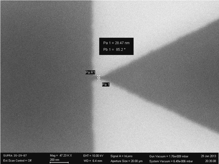
10 A CLOSER LOOK VIA SEM
11 Negative DC voltages A SIMPLE MODEL Positive DC voltages CPW R C CPW
12 V bias [V] R[Ω] C[pF] Resistance [Ω] Capacitance [pf]
13 I = I0[exp( V / V0 ) 1] (1) I 0 and V 0 have the values 3.65 ma and 4.68 V for the positive polarization and -2.6 ma and V for the negative polarization regime, respectively. Slightly asymmetric characteristics are typical in graphene devices and are due to graphene-substrate (in our case to graphene-cpw as well) interactions. Choosing a operating point I av and V av and developing (1) in a Taylor series, around an operating point it results the demodulating term arround (I av, V av ): ΔI = I I av = 2 VRF I0 exp( V / V 2 av 4V V RF -the value of the RF signal 0 0 ) (2)
")
14 GRAPHENE RADIO Bias tee 2 Current source (from Keithley 4200 SCS) + I V AM microwave generator Bias tee 1 CPW on graphene Amplifier (LNA) Oscilloscope
15 Input power 0 dbm Max responsivity 1100 V/W at 3.5GHz Input power 0 dbm No bias-rectenna? The detected DC voltage as a function of frequency for various DC currents: 1 ma (thin gray line), 2 ma (black line), 3 ma (thick gray line).

16 Demodulated signal in time 1 khz
 (100 nm width) Ohmic contact-pt Ti -4..3 3 ev Graphene work function -4.")
17 SCHOTTKY DIODE VIA DISSIMILAR METALS Schottky metals for graphene Metal Work function (ev) Al ev (the best) Cr -4.5 ev Schottky contact (Ti) (100 nm width) Ohmic contact-pt Ti ev Graphene work function -4.5 ev Ohmic metals for graphene Metal Work function (ev) graphene Pd Pt ev -5.6 ev

18 Our results-currents at ma level!
![Bias voltage (V) R S [Ω] R J [kω] C J [ff] 0V 60 12 3.](/docs-images/86/93183129/images/19-3.jpg "5 1V 60 8 3.5 2V 60 8 3.5 3V 60 0.85 3.5 4V 60 0.61 3.")
19 Bias voltage (V) R S [Ω] R J [kω] C J [ff] 0V V V V V

20 MEASURED SIMULATED A GRAPHENE PHASE SHIFTER
21 BALLISTIC GEOMETRIC GRAPHENE DIODE d in y rectification x d out d > in D out =100nm D in =20 nm L=200nm d out d j = d ( d d ) j /( N + 1) in in out metallic contact L metallic contact We compute: n, j = sgn( E V j ) ( E V j ) /( vf ) ( nπ / d j ) A n,j j = in,out are calculated by imposing the continuity conditions at each interface for the spinorial solutions of the Dirac equation in region j: N j [ An, j exp( ikn, j x) + Bn, j exp( ikn, j x)]sin(2nπy / d j ) Ψ (, ) = n= 1 j x y N j [ An, j exp( ikn, j x) Bn, j exp( ikn, j x)]sin(2nπy / d j ) n= 1 k V j = jev /( N +1) T = Nout N in A 2 n out A 2, n, in n= 1 n= 1 Potential energy
22 N j = Int[ d E V /( π v )] Number of modes j j F The results are independent on the number of discretization regions N. Although there are a finite number of outgoing modes for both voltage polarizations, in all cases there is a voltage range in which no charge carriers are transmitted since for these V values the number of outgoing modes, and hence the current, vanishes. This region, with a width given byπ v F / d out E F E F = 0 (blue dashed line), 0.1 ev (solid black line) and 0.2 ev (red dotted line).
23


24 PMMA 100 nm A 12-a A 12-a ediţie ediţie aa Seminarului SeminaruluiNaţional Naţionaldede Nanoştiinţă Nanoştiinţă şi Nanotehnologie, şi Nanotehnologie, Biblioteca BibliotecaAcademiei AcademieiRomâne, Române, Bucureşti Bucureşti
25 60 mv k b T=27 mev at room temperature E g =60 mev C=3 af R=10K Ω τ= 30fs fc=6 THz Phys. Rev. Lett. 98, (2007) Energy Band-Gap Engineering of Graphene Nanoribbons
26 ACKNODLEGEMENTS I would like to thank to many scientists which helped me in the quest in the area of carbon nanoelectronics, most of them being co-authors of many papers published in the last period of time. My wife Daniela has helped me with her deep knowledge in the area of quantum mechanics,solid state physics and graphene physics. My colleagues from IMT Bucharest (Alex Muller, Dan Neculoiu, Adrian Dinescu, Alina Cismaru, Antonio Radoi,), dr. George Konstantinidis from FORTH Heraklion, dr. George Deligeorgis from LAAS Toulouse were behind almost any device reported in this talk especially due to their invaluable knowledge in the area of semiconductor technology. I am grateful Prof. Hans Hartnagel who during many years has helped and guided me in the area of microwaves and nanoelectronics. This work was supported by a grant of Romanian National Authority for Scientific Research, CNCS-UEFISCDI, project number PN-II-ID-PCE , and the the European Commission for the financial support via the FP 7 NANO RF ( grant agreement
Nanoscale Diodes Without p-n Junctions
 Nanoscale Diodes Without p-n Junctions Mircea DRAGOMAN National Institute for Research and Development in Microtechnology (IMT), P.O. Box 38-160, 023573 Bucharest, Romania E-mail: mircea.dragoman@imt.ro
MICROWAVE AND MILLIMETERWAVE ELECTRICAL PERMITTIVITY OF GRAPHENE MONOLAYER. G. Konstantinidis 3
 1 MICROWAVE AND MILLIMETERWAVE ELECTRICAL PERMITTIVITY OF GRAPHENE MONOLAYER Alina Cismaru 1, Mircea Dragoman 1*, Adrian Dinescu 1, Daniela Dragoman 2, G. Stavrinidis, G. Konstantinidis 3 1 National Institute
Ph.D. students, postdocs, and young researchers, which need to absorb a lot of new knowledge, not taught at universities, in a rather short time.
 We have started to work in the area of graphene at the end of 2006, discovering that the fascinating Dirac equations could drive to new discoveries in solid-state physics. At that time, although the Dirac
Graphene A One-Atom-Thick Material for Microwave Devices
 ROMANIAN JOURNAL OF INFORMATION SCIENCE AND TECHNOLOGY Volume 11, Number 1, 2008, 29 35 Graphene A One-Atom-Thick Material for Microwave Devices D. DRAGOMAN 1, M. DRAGOMAN 2, A. A. MÜLLER3 1 University
DETECTION OF ELECTROMAGNETIC WAVES WITH A SINGLE CARBON ATOM SHEET
 THE PUBLISHING HOUSE PROCEEDINGS OF THE ROMANIAN ACADEMY, Series A, OF THE ROMANIAN ACADEMY Volume 15, Number 2/2014, pp. 208 215 DETECTION OF ELECTROMAGNETIC WAVES WITH A SINGLE CARBON ATOM SHEET Mircea
NEGATIVE DIFFERENTIAL RESISTANCE IN GRAPHENE-BASED BALLISTIC FIELD-EFFECT-TRANSISTOR WITH OBLIQUE TOP GATE Bucharest, Romania,
 1 NEGATIVE DIFFERENTIAL RESISTANCE IN GRAPHENE-BASED BALLISTIC FIELD-EFFECT-TRANSISTOR WITH OBLIQUE TOP GATE Mircea Dragoman 1*, Adrian Dinescu 1, and Daniela Dragoman 2 1 National Institute for Research
ELECTRONIC DEVICES BASED ON CARBON NANOTUBES AND GRAPHENE
 THE PUBLISHING HOUSE PROCEEDINGS OF THE ROMANIAN ACADEMY, Series A, OF THE ROMANIAN ACADEMY Volume 10, Number 1/2009, pp. 000 000 ELECTRONIC DEVICES BASED ON CARBON NANOTUBES AND GRAPHENE Mircea DRAGOMAN
Overview. Carbon in all its forms. Background & Discovery Fabrication. Important properties. Summary & References. Overview of current research
 Graphene Prepared for Solid State Physics II Pr Dagotto Spring 2009 Laurene Tetard 03/23/09 Overview Carbon in all its forms Background & Discovery Fabrication Important properties Overview of current
NANOELECTRONICS ON A SINGLE ATOM SHEET
 Romanian Reports in Physics, Vol. 65, No. 3, P. 792 804, 2013 Dedicated to Professor Valentin I. Vlad s 70 th Anniversary NANOELECTRONICS ON A SINGLE ATOM SHEET MIRCEA DRAGOMAN National Institute for Research
Wafer-scale fabrication of graphene
 Wafer-scale fabrication of graphene Sten Vollebregt, MSc Delft University of Technology, Delft Institute of Mircosystems and Nanotechnology Delft University of Technology Challenge the future Delft University
ROOM TEMPERATURE ON-WAFER BALLISTIC GRAPHENE FIELD- EFFECT-TRANSISTOR WITH OBLIQUE DOUBLE-GATE , Bucharest, Romania, Romania
 1 ROOM TEMPERATURE ON-WAFER BALLISTIC GRAPHENE FIELD- EFFECT-TRANSISTOR WITH OBLIQUE DOUBLE-GATE Mircea Dragoman 1*, Adrian Dinescu 1, and Daniela Dragoman 2,3 1 National Institute for Research and Development
TRANSVERSE SPIN TRANSPORT IN GRAPHENE
 International Journal of Modern Physics B Vol. 23, Nos. 12 & 13 (2009) 2641 2646 World Scientific Publishing Company TRANSVERSE SPIN TRANSPORT IN GRAPHENE TARIQ M. G. MOHIUDDIN, A. A. ZHUKOV, D. C. ELIAS,
Graphene for Microwaves
 T hese days, electronics are moving toward faster, smaller, more efficient, yet cost effective, solutions. In doing so, the limits of what materials are currently available within the technologies are
Carbon based Nanoscale Electronics
 Carbon based Nanoscale Electronics 09 02 200802 2008 ME class Outline driving force for the carbon nanomaterial electronic properties of fullerene exploration of electronic carbon nanotube gold rush of
Transport through Andreev Bound States in a Superconductor-Quantum Dot-Graphene System
 Transport through Andreev Bound States in a Superconductor-Quantum Dot-Graphene System Nadya Mason Travis Dirk, Yung-Fu Chen, Cesar Chialvo Taylor Hughes, Siddhartha Lal, Bruno Uchoa Paul Goldbart University
NiCl2 Solution concentration. Etching Duration. Aspect ratio. Experiment Atmosphere Temperature. Length(µm) Width (nm) Ar:H2=9:1, 150Pa
 Width (nm) Ar:H2=9:1, 150Pa") Experiment Atmosphere Temperature #1 # 2 # 3 # 4 # 5 # 6 # 7 # 8 # 9 # 10 Ar:H2=9:1, 150Pa Ar:H2=9:1, 150Pa Ar:H2=9:1, 150Pa Ar:H2=9:1, 150Pa Ar:H2=9:1, 150Pa Ar:H2=9:1, 150Pa Ar:H2=9:1, 150Pa Ar:H2=9:1,
Experiment Atmosphere Temperature #1 # 2 # 3 # 4 # 5 # 6 # 7 # 8 # 9 # 10 Ar:H2=9:1, 150Pa Ar:H2=9:1, 150Pa Ar:H2=9:1, 150Pa Ar:H2=9:1, 150Pa Ar:H2=9:1, 150Pa Ar:H2=9:1, 150Pa Ar:H2=9:1, 150Pa Ar:H2=9:1,
Supporting Information. by Hexagonal Boron Nitride
 Supporting Information High Velocity Saturation in Graphene Encapsulated by Hexagonal Boron Nitride Megan A. Yamoah 1,2,, Wenmin Yang 1,3, Eric Pop 4,5,6, David Goldhaber-Gordon 1 * 1 Department of Physics,
Lecture 2. Introduction to semiconductors Structures and characteristics in semiconductors
 Lecture 2 Introduction to semiconductors Structures and characteristics in semiconductors Semiconductor p-n junction Metal Oxide Silicon structure Semiconductor contact Literature Glen F. Knoll, Radiation
A Phenomenological Model for the Quantum Capacitance of Monolayer and Bilayer Graphene Devices
 A Phenomenological Model for the Quantum Capacitance of Monolayer and Bilayer Graphene Devices George S. KLIROS Hellenic Air-orce Academy, Department of Electronics and Communication Engineering, Dekeleia
Carbon Nanotubes in Interconnect Applications
 Carbon Nanotubes in Interconnect Applications Page 1 What are Carbon Nanotubes? What are they good for? Why are we interested in them? - Interconnects of the future? Comparison of electrical properties
A. Optimizing the growth conditions of large-scale graphene films
 1 A. Optimizing the growth conditions of large-scale graphene films Figure S1. Optical microscope images of graphene films transferred on 300 nm SiO 2 /Si substrates. a, Images of the graphene films grown
Beyond silicon electronics-fets with nanostructured graphene channels with high on-off ratio and highmobility
 Beyond silicon electronics-fets with nanostructured graphene channels with high on-off ratio and highmobility M.Dragoman 1, A.Dinescu 1, and D.Dragoman 2 1 National Institute for Research and Development
Solid State Device Fundamentals
 Solid State Device Fundamentals ENS 345 Lecture Course by Alexander M. Zaitsev alexander.zaitsev@csi.cuny.edu Tel: 718 982 2812 Office 4N101b 1 Outline - Goals of the course. What is electronic device?
Probing Wigner Crystals in the 2DEG using Microwaves
 Probing Wigner Crystals in the 2DEG using Microwaves G. Steele CMX Journal Club Talk 9 September 2003 Based on work from the groups of: L. W. Engel (NHMFL), D. C. Tsui (Princeton), and collaborators. CMX
Raman spectroscopy at the edges of multilayer graphene
 Raman spectroscopy at the edges of multilayer graphene Q. -Q. Li, X. Zhang, W. -P. Han, Y. Lu, W. Shi, J. -B. Wu, P. -H. Tan* State Key Laboratory of Superlattices and Microstructures, Institute of Semiconductors,
Fermi Level Pinning at Electrical Metal Contacts. of Monolayer Molybdenum Dichalcogenides
 Supporting information Fermi Level Pinning at Electrical Metal Contacts of Monolayer Molybdenum Dichalcogenides Changsik Kim 1,, Inyong Moon 1,, Daeyeong Lee 1, Min Sup Choi 1, Faisal Ahmed 1,2, Seunggeol
3-month progress Report
 3-month progress Report Graphene Devices and Circuits Supervisor Dr. P.A Childs Table of Content Abstract... 1 1. Introduction... 1 1.1 Graphene gold rush... 1 1.2 Properties of graphene... 3 1.3 Semiconductor
Supporting Online Material for
 www.sciencemag.org/cgi/content/full/327/5966/662/dc Supporting Online Material for 00-GHz Transistors from Wafer-Scale Epitaxial Graphene Y.-M. Lin,* C. Dimitrakopoulos, K. A. Jenkins, D. B. Farmer, H.-Y.
MSE 310/ECE 340: Electrical Properties of Materials Fall 2014 Department of Materials Science and Engineering Boise State University
 MSE 310/ECE 340: Electrical Properties of Materials Fall 2014 Department of Materials Science and Engineering Boise State University Practice Final Exam 1 Read the questions carefully Label all figures
Schottky Rectifiers Zheng Yang (ERF 3017,
 ECE442 Power Semiconductor Devices and Integrated Circuits Schottky Rectifiers Zheng Yang (ERF 3017, email: yangzhen@uic.edu) Power Schottky Rectifier Structure 2 Metal-Semiconductor Contact The work function
Lecture 2. Introduction to semiconductors Structures and characteristics in semiconductors
 Lecture 2 Introduction to semiconductors Structures and characteristics in semiconductors Semiconductor p-n junction Metal Oxide Silicon structure Semiconductor contact Literature Glen F. Knoll, Radiation
Graphene devices and integration: A primer on challenges
 Graphene devices and integration: A primer on challenges Archana Venugopal (TI) 8 Nov 2016 Acknowledgments: Luigi Colombo (TI) UT Dallas and UT Austin 1 Outline Where we are Issues o Contact resistance
Classification of Solids
 Classification of Solids Classification by conductivity, which is related to the band structure: (Filled bands are shown dark; D(E) = Density of states) Class Electron Density Density of States D(E) Examples
(a) (b) Supplementary Figure 1. (a) (b) (a) Supplementary Figure 2. (a) (b) (c) (d) (e)
 (b) Supplementary Figure 1. (a) (b) (a) Supplementary Figure 2. (a) (b) (c) (d) (e)") (a) (b) Supplementary Figure 1. (a) An AFM image of the device after the formation of the contact electrodes and the top gate dielectric Al 2 O 3. (b) A line scan performed along the white dashed line
(a) (b) Supplementary Figure 1. (a) An AFM image of the device after the formation of the contact electrodes and the top gate dielectric Al 2 O 3. (b) A line scan performed along the white dashed line
For the following statements, mark ( ) for true statement and (X) for wrong statement and correct it.
 for true statement and (X) for wrong statement and correct it.") Benha University Faculty of Engineering Shoubra Electrical Engineering Department First Year communications. Answer all the following questions Illustrate your answers with sketches when necessary. The
Benha University Faculty of Engineering Shoubra Electrical Engineering Department First Year communications. Answer all the following questions Illustrate your answers with sketches when necessary. The
Center for Spintronic Materials, Interfaces, and Novel Architectures. Voltage Controlled Antiferromagnetics and Future Spin Memory
 Center for Spintronic Materials, Interfaces, and Novel Architectures Voltage Controlled Antiferromagnetics and Future Spin Memory Maxim Tsoi The University of Texas at Austin Acknowledgments: H. Seinige,
Final Examination EE 130 December 16, 1997 Time allotted: 180 minutes
 Final Examination EE 130 December 16, 1997 Time allotted: 180 minutes Problem 1: Semiconductor Fundamentals [30 points] A uniformly doped silicon sample of length 100µm and cross-sectional area 100µm 2
Conventional Paper I-2010
 Conventional Paper I-010 1. (a) Sketch the covalent bonding of Si atoms in a intrinsic Si crystal Illustrate with sketches the formation of bonding in presence of donor and acceptor atoms. Sketch the energy
Molecular Dynamics Study of Thermal Rectification in Graphene Nanoribbons
 Int J Thermophys (2012) 33:986 991 DOI 10.1007/s10765-012-1216-y Molecular Dynamics Study of Thermal Rectification in Graphene Nanoribbons Jiuning Hu Xiulin Ruan Yong P. Chen Received: 26 June 2009 / Accepted:
Conference Return Seminar- NANO2014,Moscow State University,Moscow,Russia Date: th July 2014
 Conference Return Seminar- NANO2014,Moscow State University,Moscow,Russia Date:13-1818 th July 2014 An electrochemical method for the synthesis of single and few layers graphene sheets for high temperature
Semiconductor Detectors are Ionization Chambers. Detection volume with electric field Energy deposited positive and negative charge pairs
 1 V. Semiconductor Detectors V.1. Principles Semiconductor Detectors are Ionization Chambers Detection volume with electric field Energy deposited positive and negative charge pairs Charges move in field
Graphene. Tianyu Ye November 30th, 2011
 Graphene Tianyu Ye November 30th, 2011 Outline What is graphene? How to make graphene? (Exfoliation, Epitaxial, CVD) Is it graphene? (Identification methods) Transport properties; Other properties; Applications;
Multicolor Graphene Nanoribbon/Semiconductor Nanowire. Heterojunction Light-Emitting Diodes
 Multicolor Graphene Nanoribbon/Semiconductor Nanowire Heterojunction Light-Emitting Diodes Yu Ye, a Lin Gan, b Lun Dai, *a Hu Meng, a Feng Wei, a Yu Dai, a Zujin Shi, b Bin Yu, a Xuefeng Guo, b and Guogang
SUPPLEMENTARY INFORMATION
 SUPPLEMENTARY INFORMATION DOI: 10.1038/NNANO.2011.138 Graphene Nanoribbons with Smooth Edges as Quantum Wires Xinran Wang, Yijian Ouyang, Liying Jiao, Hailiang Wang, Liming Xie, Justin Wu, Jing Guo, and
Effective masses in semiconductors
 Effective masses in semiconductors The effective mass is defined as: In a solid, the electron (hole) effective mass represents how electrons move in an applied field. The effective mass reflects the inverse
Supplementary Figure 1. Supplementary Figure 1 Characterization of another locally gated PN junction based on boron
 Supplementary Figure 1 Supplementary Figure 1 Characterization of another locally gated PN junction based on boron nitride and few-layer black phosphorus (device S1). (a) Optical micrograph of device S1.
Supplementary Figure 1 Dark-field optical images of as prepared PMMA-assisted transferred CVD graphene films on silicon substrates (a) and the one
 and the one") Supplementary Figure 1 Dark-field optical images of as prepared PMMA-assisted transferred CVD graphene films on silicon substrates (a) and the one after PBASE monolayer growth (b). 1 Supplementary Figure
Supplementary Figure 1 Dark-field optical images of as prepared PMMA-assisted transferred CVD graphene films on silicon substrates (a) and the one after PBASE monolayer growth (b). 1 Supplementary Figure
Supplementary Materials for
 advances.sciencemag.org/cgi/content/full/3/4/e1602726/dc1 Supplementary Materials for Selective control of electron and hole tunneling in 2D assembly This PDF file includes: Dongil Chu, Young Hee Lee,
Section 12: Intro to Devices
 Section 12: Intro to Devices Extensive reading materials on reserve, including Robert F. Pierret, Semiconductor Device Fundamentals EE143 Ali Javey Bond Model of Electrons and Holes Si Si Si Si Si Si Si
Supporting Information for: Electrical probing and tuning of molecular. physisorption on graphene
 Supporting Information for: Electrical probing and tuning of molecular physisorption on graphene Girish S. Kulkarni, Karthik Reddy #, Wenzhe Zang, Kyunghoon Lee, Xudong Fan *, and Zhaohui Zhong * Department
1 Name: Student number: DEPARTMENT OF PHYSICS AND PHYSICAL OCEANOGRAPHY MEMORIAL UNIVERSITY OF NEWFOUNDLAND. Fall :00-11:00
 1 Name: DEPARTMENT OF PHYSICS AND PHYSICAL OCEANOGRAPHY MEMORIAL UNIVERSITY OF NEWFOUNDLAND Final Exam Physics 3000 December 11, 2012 Fall 2012 9:00-11:00 INSTRUCTIONS: 1. Answer all seven (7) questions.
UNIVERSITY OF CALIFORNIA, BERKELEY College of Engineering Department of Electrical Engineering and Computer Sciences
 UNIVERSITY OF CALIFORNIA, BERKELEY College of Engineering Department of Electrical Engineering and Computer Sciences EE 105: Microelectronic Devices and Circuits Spring 2008 MIDTERM EXAMINATION #1 Time
UNIVERSITY OF CALIFORNIA College of Engineering Department of Electrical Engineering and Computer Sciences. EECS 130 Professor Ali Javey Fall 2006
 UNIVERSITY OF CALIFORNIA College of Engineering Department of Electrical Engineering and Computer Sciences EECS 130 Professor Ali Javey Fall 2006 Midterm 2 Name: SID: Closed book. Two sheets of notes are
Graphene and new 2D materials: Opportunities for High Frequencies applications
 Graphene and new 2D materials: Opportunities for High Frequencies applications April 21th, 2015 H. Happy, E. Pallecchi, B. Plaçais, D. Jiménez, R. Sordan, D. Neumaier Graphene Flagship WP4 HF electronic
UNIVERSITY OF CALIFORNIA College of Engineering Department of Electrical Engineering and Computer Sciences. Professor Chenming Hu.
 UNIVERSITY OF CALIFORNIA College of Engineering Department of Electrical Engineering and Computer Sciences EECS 130 Spring 2009 Professor Chenming Hu Midterm I Name: Closed book. One sheet of notes is
Theory of Electrical Characterization of Semiconductors
 Theory of Electrical Characterization of Semiconductors P. Stallinga Universidade do Algarve U.C.E.H. A.D.E.E.C. OptoElectronics SELOA Summer School May 2000, Bologna (It) Overview Devices: bulk Schottky
Supporting Information
 Supporting Information Monolithically Integrated Flexible Black Phosphorus Complementary Inverter Circuits Yuanda Liu, and Kah-Wee Ang* Department of Electrical and Computer Engineering National University
Midterm I - Solutions
 UNIVERSITY OF CALIFORNIA College of Engineering Department of Electrical Engineering and Computer Sciences EECS 130 Spring 2008 Professor Chenming Hu Midterm I - Solutions Name: SID: Grad/Undergrad: Closed
Optimizing Graphene Morphology on SiC(0001)
") Optimizing Graphene Morphology on SiC(0001) James B. Hannon Rudolf M. Tromp Graphene sheets Graphene sheets can be formed into 0D,1D, 2D, and 3D structures Chemically inert Intrinsically high carrier mobility
Optimizing Graphene Morphology on SiC(0001) James B. Hannon Rudolf M. Tromp Graphene sheets Graphene sheets can be formed into 0D,1D, 2D, and 3D structures Chemically inert Intrinsically high carrier mobility
Supplementary Figure 1. Selected area electron diffraction (SAED) of bilayer graphene and tblg. (a) AB
 of bilayer graphene and tblg. (a) AB") Supplementary Figure 1. Selected area electron diffraction (SAED) of bilayer graphene and tblg. (a) AB stacked bilayer graphene (b), (c), (d), (e), and (f) are twisted bilayer graphene with twist angle
Supplementary Figure 1. Selected area electron diffraction (SAED) of bilayer graphene and tblg. (a) AB stacked bilayer graphene (b), (c), (d), (e), and (f) are twisted bilayer graphene with twist angle
PHYSICAL ELECTRONICS(ECE3540) CHAPTER 9 METAL SEMICONDUCTOR AND SEMICONDUCTOR HETERO-JUNCTIONS
 CHAPTER 9 METAL SEMICONDUCTOR AND SEMICONDUCTOR HETERO-JUNCTIONS") PHYSICAL ELECTRONICS(ECE3540) CHAPTER 9 METAL SEMICONDUCTOR AND SEMICONDUCTOR HETERO-JUNCTIONS Tennessee Technological University Wednesday, October 30, 013 1 Introduction Chapter 4: we considered the
PHYSICAL ELECTRONICS(ECE3540) CHAPTER 9 METAL SEMICONDUCTOR AND SEMICONDUCTOR HETERO-JUNCTIONS Tennessee Technological University Wednesday, October 30, 013 1 Introduction Chapter 4: we considered the
ELECTRONIC DEVICES AND CIRCUITS SUMMARY
 ELECTRONIC DEVICES AND CIRCUITS SUMMARY Classification of Materials: Insulator: An insulator is a material that offers a very low level (or negligible) of conductivity when voltage is applied. Eg: Paper,
SUPPLEMENTARY INFORMATION
 Dirac cones reshaped by interaction effects in suspended graphene D. C. Elias et al #1. Experimental devices Graphene monolayers were obtained by micromechanical cleavage of graphite on top of an oxidized
8. Schottky contacts / JFETs
 Technische Universität Graz Institute of Solid State Physics 8. Schottky contacts / JFETs Nov. 21, 2018 Technische Universität Graz Institute of Solid State Physics metal - semiconductor contacts Photoelectric
Metal Semiconductor Contacts
 Metal Semiconductor Contacts The investigation of rectification in metal-semiconductor contacts was first described by Braun [33-35], who discovered in 1874 the asymmetric nature of electrical conduction
Solid State Device Fundamentals
 Solid State Device Fundamentals ENS 345 Lecture Course by Alexander M. Zaitsev alexander.zaitsev@csi.cuny.edu Tel: 718 982 2812 Office 4N101b 1 Outline - Goals of the course. What is electronic device?
A BIT OF MATERIALS SCIENCE THEN PHYSICS
 GRAPHENE AND OTHER D ATOMIC CRYSTALS Andre Geim with many thanks to K. Novoselov, S. Morozov, D. Jiang, F. Schedin, I. Grigorieva, J. Meyer, M. Katsnelson A BIT OF MATERIALS SCIENCE THEN PHYSICS CARBON
Center for Integrated Nanostructure Physics (CINAP)
") Center for Integrated Nanostructure Physics (CINAP) - Institute for Basic Science (IBS) was launched in 2012 by the Korean government to promote basic science in Korea - Our Center was established in 2012
Center for Integrated Nanostructure Physics (CINAP) - Institute for Basic Science (IBS) was launched in 2012 by the Korean government to promote basic science in Korea - Our Center was established in 2012
Planar Organic Photovoltaic Device. Saiful I. Khondaker
 Planar Organic Photovoltaic Device Saiful I. Khondaker Nanoscience Technology Center and Department of Physics University of Central Florida http://www.physics.ucf.edu/~khondaker W Metal 1 L ch Metal 2
Tunneling characteristics of graphene
 Tunneling characteristics of graphene Young Jun Shin, 1,2 Gopinadhan Kalon, 1,2 Jaesung Son, 1 Jae Hyun Kwon, 1,2 Jing Niu, 1 Charanjit S. Bhatia, 1 Gengchiau Liang, 1 and Hyunsoo Yang 1,2,a) 1 Department
Supplementary material for High responsivity mid-infrared graphene detectors with antenna-enhanced photo-carrier generation and collection
 Supplementary material for High responsivity mid-infrared graphene detectors with antenna-enhanced photo-carrier generation and collection Yu Yao 1, Raji Shankar 1, Patrick Rauter 1, Yi Song 2, Jing Kong
arxiv: v1 [cond-mat.mes-hall] 22 Dec 2011
![arxiv: v1 [cond-mat.mes-hall] 22 Dec 2011](/thumbs/76/73542175.jpg "arxiv: v1 [cond-mat.mes-hall] 22 Dec 2011") Direct Measurement of the Fermi Energy in Graphene Using a Double Layer Structure Seyoung Kim, 1 Insun Jo, 2 D. C. Dillen, 1 D. A. Ferrer, 1 B. Fallahazad, 1 Z. Yao, 2 S. K. Banerjee, 1 and E. Tutuc 1
Direct Measurement of the Fermi Energy in Graphene Using a Double Layer Structure Seyoung Kim, 1 Insun Jo, 2 D. C. Dillen, 1 D. A. Ferrer, 1 B. Fallahazad, 1 Z. Yao, 2 S. K. Banerjee, 1 and E. Tutuc 1
Nanoscience, MCC026 2nd quarter, fall Quantum Transport, Lecture 1/2. Tomas Löfwander Applied Quantum Physics Lab
 Nanoscience, MCC026 2nd quarter, fall 2012 Quantum Transport, Lecture 1/2 Tomas Löfwander Applied Quantum Physics Lab Quantum Transport Nanoscience: Quantum transport: control and making of useful things
Lecture 18. New gas detectors Solid state trackers
 Lecture 18 New gas detectors Solid state trackers Time projection Chamber Full 3-D track reconstruction x-y from wires and segmented cathode of MWPC z from drift time de/dx information (extra) Drift over
Ultra-low noise HEMTs for deep cryogenic lowfrequency and high-impedance readout electronics
 Ultra-low noise HEMTs for deep cryogenic lowfrequency and high-impedance readout electronics Y. Jin, Q. Dong, Y.X. Liang, A. Cavanna, U. Gennser, L Couraud - Why cryoelectronics - Why HEMT - Noise characterization
Avalanche breakdown. Impact ionization causes an avalanche of current. Occurs at low doping
 Avalanche breakdown Impact ionization causes an avalanche of current Occurs at low doping Zener tunneling Electrons tunnel from valence band to conduction band Occurs at high doping Tunneling wave decays
Gate-induced insulating state in bilayer graphene devices
 Gate-induced insulating state in bilayer graphene devices Jeroen B. Oostinga, Hubert B. Heersche, Xinglan Liu, Alberto F. Morpurgo and Lieven M. K. Vandersypen Kavli Institute of Nanoscience, Delft University
Lecture 2. Introduction to semiconductors Structures and characteristics in semiconductors. Fabrication of semiconductor sensor
 Lecture 2 Introduction to semiconductors Structures and characteristics in semiconductors Semiconductor p-n junction Metal Oxide Silicon structure Semiconductor contact Fabrication of semiconductor sensor
Schottky diodes. JFETs - MESFETs - MODFETs
 Technische Universität Graz Institute of Solid State Physics Schottky diodes JFETs - MESFETs - MODFETs Quasi Fermi level When the charge carriers are not in equilibrium the Fermi energy can be different
Electrical Characteristics of Multilayer MoS 2 FET s
 Electrical Characteristics of Multilayer MoS 2 FET s with MoS 2 /Graphene Hetero-Junction Contacts Joon Young Kwak,* Jeonghyun Hwang, Brian Calderon, Hussain Alsalman, Nini Munoz, Brian Schutter, and Michael
Introduction to Nanotechnology Chapter 5 Carbon Nanostructures Lecture 1
 Introduction to Nanotechnology Chapter 5 Carbon Nanostructures Lecture 1 ChiiDong Chen Institute of Physics, Academia Sinica chiidong@phys.sinica.edu.tw 02 27896766 Carbon contains 6 electrons: (1s) 2,
Bilayer GNR Mobility Model in Ballistic Transport Limit
 ilayer GNR Mobility Model in allistic Transport Limit S. Mahdi Mousavi, M.Taghi Ahmadi, Hatef Sadeghi, and Razali Ismail Computational Nanoelectronics (CoNE) Research Group, Electrical Engineering Faculty,
Raman Imaging and Electronic Properties of Graphene
 Raman Imaging and Electronic Properties of Graphene F. Molitor, D. Graf, C. Stampfer, T. Ihn, and K. Ensslin Laboratory for Solid State Physics, ETH Zurich, 8093 Zurich, Switzerland ensslin@phys.ethz.ch
Tunnel Diodes (Esaki Diode)
") Tunnel Diodes (Esaki Diode) Tunnel diode is the p-n junction device that exhibits negative resistance. That means when the voltage is increased the current through it decreases. Esaki diodes was named
Tunnel Diodes (Esaki Diode) Tunnel diode is the p-n junction device that exhibits negative resistance. That means when the voltage is increased the current through it decreases. Esaki diodes was named
Semiconductor Physics Problems 2015
 Semiconductor Physics Problems 2015 Page and figure numbers refer to Semiconductor Devices Physics and Technology, 3rd edition, by SM Sze and M-K Lee 1. The purest semiconductor crystals it is possible
Physics of Semiconductors
 Physics of Semiconductors 9 th 2016.6.13 Shingo Katsumoto Department of Physics and Institute for Solid State Physics University of Tokyo Site for uploading answer sheet Outline today Answer to the question
Graphene and Carbon Nanotubes
 Graphene and Carbon Nanotubes 1 atom thick films of graphite atomic chicken wire Novoselov et al - Science 306, 666 (004) 100μm Geim s group at Manchester Novoselov et al - Nature 438, 197 (005) Kim-Stormer
Electric Field-Dependent Charge-Carrier Velocity in Semiconducting Carbon. Nanotubes. Yung-Fu Chen and M. S. Fuhrer
 Electric Field-Dependent Charge-Carrier Velocity in Semiconducting Carbon Nanotubes Yung-Fu Chen and M. S. Fuhrer Department of Physics and Center for Superconductivity Research, University of Maryland,
Elementary Process of Electromigration at Metallic Nanojunctions in the Ballistic Regime
 Elementary Process of Electromigration at Metallic Nanojunctions in the Ballistic Regime Kaz Hirakawa Institute of Industrial Science, University of Tokyo CREST, JST collaborators: Akinori Umeno, Kenji
electronics fundamentals
 electronics fundamentals circuits, devices, and applications THOMAS L. FLOYD DAVID M. BUCHLA Lesson 1: Diodes and Applications Semiconductors Figure 1-1 The Bohr model of an atom showing electrons in orbits
Electrostatics of Nanowire Transistors
 Electrostatics of Nanowire Transistors Jing Guo, Jing Wang, Eric Polizzi, Supriyo Datta and Mark Lundstrom School of Electrical and Computer Engineering Purdue University, West Lafayette, IN, 47907 ABSTRACTS
EN2912C: Future Directions in Computing Lecture 08: Overview of Near-Term Emerging Computing Technologies
 EN2912C: Future Directions in Computing Lecture 08: Overview of Near-Term Emerging Computing Technologies Prof. Sherief Reda Division of Engineering Brown University Fall 2008 1 Near-term emerging computing
Spring Semester 2012 Final Exam
 Spring Semester 2012 Final Exam Note: Show your work, underline results, and always show units. Official exam time: 2.0 hours; an extension of at least 1.0 hour will be granted to anyone. Materials parameters
Intrinsic Electronic Transport Properties of High. Information
 Intrinsic Electronic Transport Properties of High Quality and MoS 2 : Supporting Information Britton W. H. Baugher, Hugh O. H. Churchill, Yafang Yang, and Pablo Jarillo-Herrero Department of Physics, Massachusetts
EE 5344 Introduction to MEMS CHAPTER 5 Radiation Sensors
 EE 5344 Introduction to MEMS CHAPTER 5 Radiation Sensors 5. Radiation Microsensors Radiation µ-sensors convert incident radiant signals into standard electrical out put signals. Radiant Signals Classification
1. Nanotechnology & nanomaterials -- Functional nanomaterials enabled by nanotechnologies.
 Novel Nano-Engineered Semiconductors for Possible Photon Sources and Detectors NAI-CHANG YEH Department of Physics, California Institute of Technology 1. Nanotechnology & nanomaterials -- Functional nanomaterials
Semi-insulating SiC substrates for high frequency devices
 Klausurtagung Silberbach, 19. - 21. Feb. 2002 Institut für Werkstoffwissenschaften - WW 6 Semi-insulating SiC substrates for high frequency devices Vortrag von Matthias Bickermann Semi-insulating SiC substrates
2) Atom manipulation. Xe / Ni(110) Model: Experiment:
 Atom manipulation. Xe / Ni(110) Model: Experiment:") 2) Atom manipulation D. Eigler & E. Schweizer, Nature 344, 524 (1990) Xe / Ni(110) Model: Experiment: G.Meyer, et al. Applied Physics A 68, 125 (1999) First the tip is approached close to the adsorbate
2) Atom manipulation D. Eigler & E. Schweizer, Nature 344, 524 (1990) Xe / Ni(110) Model: Experiment: G.Meyer, et al. Applied Physics A 68, 125 (1999) First the tip is approached close to the adsorbate
OPTI510R: Photonics. Khanh Kieu College of Optical Sciences, University of Arizona Meinel building R.626
 OPTI510R: Photonics Khanh Kieu College of Optical Sciences, University of Arizona kkieu@optics.arizona.edu Meinel building R.626 Announcements Homework #6 is assigned, due May 1 st Final exam May 8, 10:30-12:30pm
Contact Engineering of Two-Dimensional Layered Semiconductors beyond Graphene
 Contact Engineering of Two-Dimensional Layered Semiconductors beyond Graphene Zhixian Zhou Department of Physics and Astronomy Wayne State University Detroit, Michigan Outline Introduction Ionic liquid