TWO- AND THREE-QUBIT ROOM-TEMPERATURE GRAPHENE QUANTUM GATES. Daniela Dragoman 1 and Mircea Dragoman Bucharest, Romania
|
|
|
- Pamela Shelton
- 6 years ago
- Views:
Transcription
1 1 TWO- AND THREE-QUBIT ROOM-TEMPERATURE GRAPHENE QUANTUM GATES Daniela Dragoman 1 and Mircea Dragoman 2 1 Univ. Bucharest, Faculty of Physics, P.O. Box MG-11, Bucharest, Romania 2 National Institute for Research and Development in Microtechnology (IMT), P.O. Box , Bucharest, Romania Abstract Proposed configurations for the implementation of graphene-based CNOT and Toffoli gates working at room temperature are presented. These two logic gates, essential for any quantum computing algorithm, involve ballistic Y junctions for qubit implementation, quantum interference for qubit interaction and oblique gates for optimizing the output, and can be fabricated using existing nanolitographical techniques. The proposed configurations of CNOT and Toffoli quantum logic gates are based on the very large mean-free-paths of carriers in graphene at room temperature.
2 2 Quantum computers promise massive parallel computation with the help of quantum gates, which process quantum bits, known as qubits [1]. The implementation, manipulation and read-out of qubits, which are a superposition of states governed by the laws of quantum mechanics, is completely different from that of the classical bits 0 and 1, implemented by transistors with two switching states. However, despite the impressive progress in the implementation of quantum gates and algorithms [2], quantum computer technology is very far from superseding classical computation, which has attained a high degree of integration, of about one billion transistors on a single silicon chip. The main difficulty faced by quantum computation is the rapid loss of coherence of quantum states, attempts to alleviate this problem including the use of atomic clock transitions [3] and quantum error correction algorithms [4]. Many solutions to overcome quantum decoherence and to assure integration and miniaturization of solid-state quantum computers have been proposed in the last years. Promising results have been obtained, for example, using the well-developed semiconductor nanotechnology, especially the silicon nanotechnology [5], and in superconductors [4], where quantum circuits containing thousands of elements on a chip were fabricated. Spin qubits, in particular, have received a lot of attention [6-9]. Even if the decoherence time is now as large as a few seconds, allowing tens of thousands of qubit operations to be performed [2,6], the presentday solid-state quantum computing systems work at extreme low temperatures (not to mention other requirements on pressure, magnetic fields, etc.), such that a commercially available quantum computer is still far away. New hope has emerged with the discovery of graphene, in which charge carriers obey unique physical principles. Proposals of quantum computation based on spin qubits in graphene nanoribbons [10], graphene quantum dots [11], and graphene antidot lattices [12] require extremely small temperatures and/or specific carving of the graphene sheet, while valley-based qubits [13] require particular magnetic field configurations.
3 3 In this paper we propose an implementation of room-temperature two- and three-qubit logic gates in graphene based on the ballistic transport regime in this material, without the requirement of additional magnetic fields. The 0 and 1 quantum states are encoded using Y- branch switches [14,15], and the coupling between qubits is optimized using oblique electrostatic gates. We have demonstrated recently that ballistic graphene field effect transistors using oblique electrostatic gates can be fabricated on 60-70% of the surface of a 4 inch wafer chip covered with graphene monolayer grown by CVD [16], which demonstrates that the technology to fabricate our proposed graphene-based quantum gates shows relatively high reproducibility on large surfaces. Thus, circuits containing successions of quantum graphene gates could be fabricated on such areas, with minimum nanolithography features of about nm and even less, the room-temperature ballistic transport regime in high-quality graphene monolayers being preserved for mean-free paths of up to 400 nm if graphene is deposited on SiO 2, or up to 1 m in graphene deposited over boron nitride [17]. Very recently, it was demonstrated that these already impressive mean-free paths at room temperatures could attain even larger values, of more than 10 m [18], for nm wide graphene nanoribbons epitaxially grown on SiC. Such huge room-temperature mean-free paths are the main advantage of graphene over any other materials, which could eventually attain comparable mean-free path values only at very low temperatures. This advantage implies that quantum circuits based on ballistic transport in graphene could be easily fabricated using standard nanolithography methods, such as electron-beam lithography. The schematic configuration of a two-qubit CNOT graphene gate is represented in Fig. 1. It consists of two nanoribbons, corresponding to the two entries: the control qubit C and the input qubit denoted by in in Fig. 1, which interact/interfere in a region of length L and width W when the control qubit is in the logic state. The two logic states of C, 0 and, are identified with the outputs of the Y-junction following the entry C, the charge carriers with the wavefunction passing also through a region in which an electrostatic potential V G induced by an oblique gate modifies their amplitude and phase. Note that the Y-junction implements also
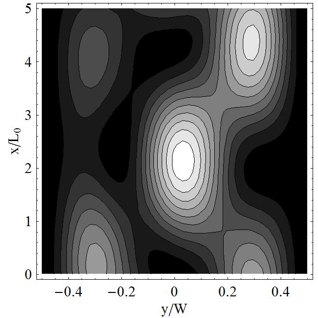
4 4 the superposition of the logic states 0 and, essential for quantum computing [14,15]. The inset in Fig. 1 illustrates the dependence of the transmission coefficient 2 T t through the gate on V G for electrons with energy E = 0.1 ev, an incidence angle of 15 o and a gate length L 0 = 50 nm. Assuming that the width of the interference region is W = 100 nm, and that the wavefunction in the input nanoribbon i, with i = 1,2, has the form ( y; y, y) a i i i exp[ ( y y ) i 6 /( y) 6 ], we have represented in Figs. 2(a) and 2(b) the evolution of the modulus of the wavefunction in the interference region as a function of x for the cases when the logical value of the control bit is 0 and, respectively. In these simulations a1 t, y1 W / 4 for the input corresponding to the logical value of C ( a 1 = 0 when C is 0 ) and a 2 1, y2 W / 4 for the in qubit and y W / 7. 5 in both cases, V G = 40 mev, the incidence angle on the oblique gate is 15 o, and a phase difference between the wavefunction of the C and in qubits corresponding to a difference between path lengths L = 10 nm was considered. In calculating the wavefunction in the interference region, we have added the contribution of each mode in the interference region. In order to implement a CNOT gate, the two outputs, out1 and out2, with definite logic states, should interchange their logic states when the control qubit is. Assuming that the output nanoribbons are identical, the fraction of the total transmission coefficient in these nanoribbons, denoted by T 1 and T 2, respectively, are shown in Fig. 3 as a function of the length of the interference region L. The red and blue curves represent T 1 and, respectively, T 2, while with solid and dotted lines we have illustrated the cases when the logic values of C are, correspondingly, and 0. The transmission fractions T 1 and T 2 (as well as the form and evolution of the total wavefunction in the interference region) depend on the voltage applied on the oblique gate and the angle of incidence. These parameters can be chosen such that T 1 and T 2 are separated as well as possible for a given L value. For an unambiguous operation of the
5 5 CNOT gate, the logical states of out1 and out2 can be well defined if the dotted (and solid) curves of different colors are well separated and if the dotted curves are well separated from the solid curves of the same color. This can be achieved in our CNOT configuration if L 3L0 = 150 nm. Over propagation lengths of about 150 nm the transport should be ballistic, condition that could easily be met in graphene-based devices. Under these conditions, logical values and 0 (or vice-versa) can be assigned to out1 and out2, respectively, if T and T , these two values being interchanged if C is in the state. To implement the universal three-qubit Toffoli gate, for example, we need three entries: two control qubits, C1 and C2 and an input qubit in, the interaction between them interchanging the logical value of in only when both C1 and C2 are in the state. A possible graphene-based implementation of such a Toffoli gate is represented in Fig. 4, Y-junctions being again used to define the logical states of the control bits and the output states with well defined logic values. In this configuration, the in qubit interacts in the interference region of width W and length L with control qubits when the logic states of C1 and C2 are 10, 01 and 11. We can distinguish between these cases assuming that in the first two situations a 1 (1/ 2) t and in the last one a t 1. Then, the evolution of the modulus of the wavefunction in the interference region when the logic states of C1 and C2 are 00, 10 or 01, and 11 are illustrated in Figs. 5(a)-(c), respectively, for the same parameters as above, except that V G = 45 mev and L = 20 nm. The corresponding fractions of the transmitted coefficient collected by the outputs out1 and out2 are represented in Fig. 6 with red and blue curves, respectively, as a function of the length of the interference region L. The solid, dotted and dashed-dotted lines correspond to the cases when the logic states of C1 and C2 are 11, 00, and 10 or 01, respectively. For the Toffoli gate, unambiguous computing is achieved when the solid lines for each color are well separated from the dotted and dashed-dotted lines of the same color, condition that can be achieved for small L values, L 1.5L0 = 75 nm; ballistic transport over such propagation lengths is not difficult to
6 6 achieve. For the example chosen in the simulations in Fig. 6, the logical values and 0 (or vice-versa) can be assigned to out1 and out2, respectively, if T and T , respectively, these values being interchanged if both C1 and C2 are in the logical state. In conclusion, we have demonstrated that room-temperature CNOT and Toffoli logic gates can be implemented using the ballistic transport regime in graphene. These quantum gates can then be cascaded and form quantum circuits, the decoherence being avoided as long as the total dimension of the circuit is smaller than the mean-free path, parameter which takes a very large value in graphene, even at room temperature. The proposed configurations of CNOT and Toffoli gates are based on Y junctions to achieve superpositions of quantum logic states and on interference regions to assure interactions between qubits. Oblique gates are used in both cases to optimize the outputs. The CNOT and Toffoli gates can be implemented at room temperature with the existing nanotechnologies of a standard clean room, while the input, manipulation and readout of these quantum gates involve measurements of charge flow and application of gate voltages, procedures that are well controlled experimentally.
7 7 References [1] M.A. Nielsen, I.L. Chuang, Quantum Computation and Quantum Information, 10 th Edition, Cambridge Univ. Press, Cambridge, U.K. (2010). [2] T.D. Ladd, F. Jelezko, R. Laflamme, Y. Nakamura, C. Monroe, J.L. O Brien, Quantum computers, Nature 464, (2010). [3] G. Wolfowicz, A.M. Tyryshkin, R.E. George, H. Riemann, N.V. Abrosimov, P. Becker, H,-J, Pohl, M.L.W. Thewalt, S.A. Lyon, J.J.L. Morton, Atomic clock transitions in silicon-based spin qubits, Nature Nanotechnology 8, (2013). [4] M.H. Devoret, R.J. Schoelkopf, Superconducting circuits for quantum information: an outlook, Science 329, (2013). [5] F.A. Zwanenburg, A.S. Dzurak, A. Morello, M.Y. Simmons, C.L. Hollenberg, G. Klimeck, S. Rogge, S.N. Coppersmith, M.A. Eriksson, Silicon quantum electronics, Rev. Mod. Phys. 85, (2013). [6] D.D. Awshalom, L.C. Basset, A.D. Dzurak, E.L. Hu, J.R. Petta, Quantum spintronics: engineering and manipulating atom-like spins in semiconductors, Science 339, (2013). [7] J.J.L. Morton, D.R. McCarney, M.A. Eriksson, S.A. Lyon, Embracing the quantum limit in silicon computing, Nature 479, (2011). [8] C. Kloeffel, D. Loss, Prospects for spin-based quantum computing in quantum dots, Annual Review of Condensed Matter Physics 4, (2013). [9] M. Fuechsle, J.A. Miwa, S. Mahapatra, H. Ryu, S. Lee, O.Warschkow, L.C.L. Hollenberg, G. Klimeck, M.Y. Simmons, A single-atom transistor, Nature Nanotechnology 7, (2012). [10] G.-P. Guo, Z.-R. Lin, T. Tu, G. Cao, X.-P. Li, G.-C. Guo, Quantum computation with graphene nanoribbon, New J. Phys. 11, (2009).
8 8 [11] B. Trauzettel, D.V. Bulaev, D. Loss, G. Burkard, Spin qubits in graphene quantum dots, Nature Physics 3, (2007). [12] T.G. Pedersen, C. Flindt, J. Pedersen, N.A. Mortensen, A.-P. Jauho, K. Pedersen, Graphene antidot lattices: designed defects and spin qubits, Phys. Rev. Lett. 100, (2008). [13] G.Y. Wu, N.-Y. Lue, Graphene-based qubits in quantum communications, Phys. Rev. B 86, (2012). [14] O.A. Tkachenko, V.A. Tkachenko, Z.D. Kvon, A.L. Aseev, J.-C. Portal, Quantum interferential Y-junction switch, Nanotechnology 23, (2012). [15] G.M. Jones, C.H. Yang, M.J. Yang, Y.B. Lyanda-Geller, Quantum steering of electron wave function in an InAs Y-branch switch, Appl. Phys. Lett. 86, (2005). [16] M. Dragoman, A. Dinescu, D. Dragoman, Negative differential resistance in graphenebased ballistic field effect transistor with oblique top gate, Nanotechnolgy 25, (2014). [17] A.S. Mayorov, R.V. Gorbachev, S.V. Morozov, L. Britnell, R. Jail, L.A. Ponomarenko, K.S. Novoselov, K. Watanabe, T. Taniguchi, A.K. Geim, Micrometer-scale ballistic transport in encapsulated graphene at room temperature, Nano Lett. 11, 2396 (2011). [18] J. Baringhaus, J.M. Ruan, F. Edler, A. Tejeda, M. Sicot, A.Taleb-Ibrahimi, A.-P. Li, Z. Jiang, E.H. Conrad, C. Berger, C. Tegenkamp, and W.A. de Heer, Exceptional ballistic transport in epitaxial graphene nanoribbons, Nature 506, (2014).
9 9 Figure Captions Fig. 1 Schematic configuration of a two-qubit CNOT graphene gate. Inset: Dependence of the transmission coefficient on the potential energy on an oblique gate. Fig. 2 Evolution of the modulus of the wavefunction in the interference region for the cases when the logical value of the control bit is (a) 0 and (b). Fig. 3 Fraction of the total transmission coefficient in the output nanoribbons, T 1 (red lines) and T 2 (blue lines), as a function of the length of the interference region when the logic values of C are (solid lines) and 0 (dotted lines). Fig. 4 Schematic representation of a graphene-based Toffoli gate. Fig. 5 Evolution of the modulus of the wavefunction in the interference region when the logic states of C1 and C2 are (a) 00, (b) 10 or 01, and (c) 11. Fig. 6 Fraction of the transmitted coefficient collected by the outputs out1 (red lines) and out2 (blue lines) as a function of the length of the interference region when the logic states of C1 and C2 are 11 (solid lines), 00 (dotted lines), and 10 or 01 (dashed-dotted lines).
10 10 0> C gate L 0 1> out1 in W y x substrate graphene L out2 Fig. 1
 Fig.")
11 11 (a) (b) Fig. 2
12 12 Fig. 3 substrate 0> 0> C1 C2 1> 1> out1 gate graphene x y W in out2 L Fig. 4
")
13 13 (a) (b) Fig. 5 (c)
14 Fig. 6 14
ROOM TEMPERATURE ON-WAFER BALLISTIC GRAPHENE FIELD- EFFECT-TRANSISTOR WITH OBLIQUE DOUBLE-GATE , Bucharest, Romania, Romania
 1 ROOM TEMPERATURE ON-WAFER BALLISTIC GRAPHENE FIELD- EFFECT-TRANSISTOR WITH OBLIQUE DOUBLE-GATE Mircea Dragoman 1*, Adrian Dinescu 1, and Daniela Dragoman 2,3 1 National Institute for Research and Development
MICROWAVE AND MILLIMETERWAVE ELECTRICAL PERMITTIVITY OF GRAPHENE MONOLAYER. G. Konstantinidis 3
 1 MICROWAVE AND MILLIMETERWAVE ELECTRICAL PERMITTIVITY OF GRAPHENE MONOLAYER Alina Cismaru 1, Mircea Dragoman 1*, Adrian Dinescu 1, Daniela Dragoman 2, G. Stavrinidis, G. Konstantinidis 3 1 National Institute
NEGATIVE DIFFERENTIAL RESISTANCE IN GRAPHENE-BASED BALLISTIC FIELD-EFFECT-TRANSISTOR WITH OBLIQUE TOP GATE Bucharest, Romania,
 1 NEGATIVE DIFFERENTIAL RESISTANCE IN GRAPHENE-BASED BALLISTIC FIELD-EFFECT-TRANSISTOR WITH OBLIQUE TOP GATE Mircea Dragoman 1*, Adrian Dinescu 1, and Daniela Dragoman 2 1 National Institute for Research
Graphene A One-Atom-Thick Material for Microwave Devices
 ROMANIAN JOURNAL OF INFORMATION SCIENCE AND TECHNOLOGY Volume 11, Number 1, 2008, 29 35 Graphene A One-Atom-Thick Material for Microwave Devices D. DRAGOMAN 1, M. DRAGOMAN 2, A. A. MÜLLER3 1 University
Beyond silicon electronics-fets with nanostructured graphene channels with high on-off ratio and highmobility
 Beyond silicon electronics-fets with nanostructured graphene channels with high on-off ratio and highmobility M.Dragoman 1, A.Dinescu 1, and D.Dragoman 2 1 National Institute for Research and Development
Ph.D. students, postdocs, and young researchers, which need to absorb a lot of new knowledge, not taught at universities, in a rather short time.
 We have started to work in the area of graphene at the end of 2006, discovering that the fascinating Dirac equations could drive to new discoveries in solid-state physics. At that time, although the Dirac
Monolayer Semiconductors
 Monolayer Semiconductors Gilbert Arias California State University San Bernardino University of Washington INT REU, 2013 Advisor: Xiaodong Xu (Dated: August 24, 2013) Abstract Silicon may be unable to
Enhancement-mode quantum transistors for single electron spin
 Purdue University Purdue e-pubs Other Nanotechnology Publications Birck Nanotechnology Center 8-1-2006 Enhancement-mode quantum transistors for single electron spin G. M. Jones B. H. Hu C. H. Yang M. J.
Martes cuántico Zaragoza, 8 th October Atomic and molecular spin qubits. Fernando LUIS Instituto de Ciencia de Materiales de Aragón
 Martes cuántico Zaragoza, 8 th October 2013 Atomic and molecular spin qubits Fernando LUIS Instituto de Ciencia de Materiales de Aragón Outline Quantum information with spins 1 0 Atomic defects in semiconductors
Supporting Information. by Hexagonal Boron Nitride
 Supporting Information High Velocity Saturation in Graphene Encapsulated by Hexagonal Boron Nitride Megan A. Yamoah 1,2,, Wenmin Yang 1,3, Eric Pop 4,5,6, David Goldhaber-Gordon 1 * 1 Department of Physics,
The Development of a Quantum Computer in Silicon
 The Development of a Quantum Computer in Silicon Professor Michelle Simmons Director, Centre of Excellence for Quantum Computation and Communication Technology, Sydney, Australia December 4th, 2013 Outline
Nanoscale Diodes Without p-n Junctions
 Nanoscale Diodes Without p-n Junctions Mircea DRAGOMAN National Institute for Research and Development in Microtechnology (IMT), P.O. Box 38-160, 023573 Bucharest, Romania E-mail: mircea.dragoman@imt.ro
phys4.20 Page 1 - the ac Josephson effect relates the voltage V across a Junction to the temporal change of the phase difference
 Josephson Effect - the Josephson effect describes tunneling of Cooper pairs through a barrier - a Josephson junction is a contact between two superconductors separated from each other by a thin (< 2 nm)
SiC Graphene Suitable For Quantum Hall Resistance Metrology.
 SiC Graphene Suitable For Quantum Hall Resistance Metrology. Samuel Lara-Avila 1, Alexei Kalaboukhov 1, Sara Paolillo, Mikael Syväjärvi 3, Rositza Yakimova 3, Vladimir Fal'ko 4, Alexander Tzalenchuk 5,
TRANSVERSE SPIN TRANSPORT IN GRAPHENE
 International Journal of Modern Physics B Vol. 23, Nos. 12 & 13 (2009) 2641 2646 World Scientific Publishing Company TRANSVERSE SPIN TRANSPORT IN GRAPHENE TARIQ M. G. MOHIUDDIN, A. A. ZHUKOV, D. C. ELIAS,
Circuit Quantum Electrodynamics. Mark David Jenkins Martes cúantico, February 25th, 2014
 Circuit Quantum Electrodynamics Mark David Jenkins Martes cúantico, February 25th, 2014 Introduction Theory details Strong coupling experiment Cavity quantum electrodynamics for superconducting electrical
ROOM TEMPERATURE NANOSTRUCTURED GRAPHENE TRANSISTOR WITH HIGH ON/OFF RATIO Bucharest, Romania,
 1 ROOM TEMPERATURE NANOSTRUCTURE GRAPHENE TRANSISTOR WITH HIGH ON/OFF RATIO Mircea ragoman 1*, Adrian inescu 1, and aniela ragoman 2,3 1 National Institute for Research and evelopment in Microtechnology
NiCl2 Solution concentration. Etching Duration. Aspect ratio. Experiment Atmosphere Temperature. Length(µm) Width (nm) Ar:H2=9:1, 150Pa
 Width (nm) Ar:H2=9:1, 150Pa") Experiment Atmosphere Temperature #1 # 2 # 3 # 4 # 5 # 6 # 7 # 8 # 9 # 10 Ar:H2=9:1, 150Pa Ar:H2=9:1, 150Pa Ar:H2=9:1, 150Pa Ar:H2=9:1, 150Pa Ar:H2=9:1, 150Pa Ar:H2=9:1, 150Pa Ar:H2=9:1, 150Pa Ar:H2=9:1,
Experiment Atmosphere Temperature #1 # 2 # 3 # 4 # 5 # 6 # 7 # 8 # 9 # 10 Ar:H2=9:1, 150Pa Ar:H2=9:1, 150Pa Ar:H2=9:1, 150Pa Ar:H2=9:1, 150Pa Ar:H2=9:1, 150Pa Ar:H2=9:1, 150Pa Ar:H2=9:1, 150Pa Ar:H2=9:1,
Exceptional ballistic transport in epigraphene. Walt de Heer Georgia Institute of Technology
 Exceptional ballistic transport in epigraphene Walt de Heer Georgia Institute of Technology Program Objective First formulated in 2001 and patented in 2003, our objective is to develop nanoelectronics
Supercondcting Qubits
 Supercondcting Qubits Patricia Thrasher University of Washington, Seattle, Washington 98195 Superconducting qubits are electrical circuits based on the Josephson tunnel junctions and have the ability to
2.0 Basic Elements of a Quantum Information Processor. 2.1 Classical information processing The carrier of information
 QSIT09.L03 Page 1 2.0 Basic Elements of a Quantum Information Processor 2.1 Classical information processing 2.1.1 The carrier of information - binary representation of information as bits (Binary digits).
Transport properties through double-magnetic-barrier structures in graphene
 Chin. Phys. B Vol. 20, No. 7 (20) 077305 Transport properties through double-magnetic-barrier structures in graphene Wang Su-Xin( ) a)b), Li Zhi-Wen( ) a)b), Liu Jian-Jun( ) c), and Li Yu-Xian( ) c) a)
IS THERE ANY KLEIN PARADOX? LOOK AT GRAPHENE! D. Dragoman Univ. Bucharest, Physics Dept., P.O. Box MG-11, Bucharest,
 1 IS THERE ANY KLEIN PARADOX? LOOK AT GRAPHENE! D. Dragoman Univ. Bucharest, Physics Dept., P.O. Box MG-11, 077125 Bucharest, Romania, e-mail: danieladragoman@yahoo.com Abstract It is demonstrated that
Quantum transport through graphene nanostructures
 Quantum transport through graphene nanostructures S. Rotter, F. Libisch, L. Wirtz, C. Stampfer, F. Aigner, I. Březinová, and J. Burgdörfer Institute for Theoretical Physics/E136 December 9, 2009 Graphene
Intrinsic Electronic Transport Properties of High. Information
 Intrinsic Electronic Transport Properties of High Quality and MoS 2 : Supporting Information Britton W. H. Baugher, Hugh O. H. Churchill, Yafang Yang, and Pablo Jarillo-Herrero Department of Physics, Massachusetts
DEVELOPING A QUANTUM CIRCUIT SIMULATOR API
 ACTA UNIVERSITATIS CIBINIENSIS TECHNICAL SERIES Vol. LXVII 2015 DOI: 10.1515/aucts-2015-0084 DEVELOPING A QUANTUM CIRCUIT SIMULATOR API MIHAI DORIAN Stancu Ph.D. student, Faculty of Economic Sciences/Cybernetics
GaAs and InGaAs Single Electron Hex. Title. Author(s) Kasai, Seiya; Hasegawa, Hideki. Citation 13(2-4): Issue Date DOI
 Kasai, Seiya; Hasegawa, Hideki. Citation 13(2-4): Issue Date DOI") Title GaAs and InGaAs Single Electron Hex Circuits Based on Binary Decision D Author(s) Kasai, Seiya; Hasegawa, Hideki Citation Physica E: Low-dimensional Systems 3(2-4): 925-929 Issue Date 2002-03 DOI
Title GaAs and InGaAs Single Electron Hex Circuits Based on Binary Decision D Author(s) Kasai, Seiya; Hasegawa, Hideki Citation Physica E: Low-dimensional Systems 3(2-4): 925-929 Issue Date 2002-03 DOI
Introduction to Nanotechnology Chapter 5 Carbon Nanostructures Lecture 1
 Introduction to Nanotechnology Chapter 5 Carbon Nanostructures Lecture 1 ChiiDong Chen Institute of Physics, Academia Sinica chiidong@phys.sinica.edu.tw 02 27896766 Carbon contains 6 electrons: (1s) 2,
Quantum Computing An Overview
 Quantum Computing An Overview NAS Division NASA Ames Research Center TR Govindan Program Manager, QIS U.S. Army Research Office Outline Motivation Essentials of the Quantum Computing (QC) model Challenges
Evaluation of Electronic Characteristics of Double Gate Graphene Nanoribbon Field Effect Transistor for Wide Range of Temperatures
 Evaluation of Electronic Characteristics of Double Gate Graphene Nanoribbon Field Effect Transistor for Wide Range of Temperatures 1 Milad Abtin, 2 Ali Naderi 1 Department of electrical engineering, Masjed
SUPPLEMENTARY INFORMATION
 Dirac cones reshaped by interaction effects in suspended graphene D. C. Elias et al #1. Experimental devices Graphene monolayers were obtained by micromechanical cleavage of graphite on top of an oxidized
Wafer-scale fabrication of graphene
 Wafer-scale fabrication of graphene Sten Vollebregt, MSc Delft University of Technology, Delft Institute of Mircosystems and Nanotechnology Delft University of Technology Challenge the future Delft University
Graphene devices and integration: A primer on challenges
 Graphene devices and integration: A primer on challenges Archana Venugopal (TI) 8 Nov 2016 Acknowledgments: Luigi Colombo (TI) UT Dallas and UT Austin 1 Outline Where we are Issues o Contact resistance
3-month progress Report
 3-month progress Report Graphene Devices and Circuits Supervisor Dr. P.A Childs Table of Content Abstract... 1 1. Introduction... 1 1.1 Graphene gold rush... 1 1.2 Properties of graphene... 3 1.3 Semiconductor
Lecture 0: Introduction
 Lecture 0: Introduction Introduction q Integrated circuits: many transistors on one chip q Very Large Scale Integration (VLSI): bucketloads! q Complementary Metal Oxide Semiconductor Fast, cheap, low power
Supplementary Figure 1. Supplementary Figure 1 Characterization of another locally gated PN junction based on boron
 Supplementary Figure 1 Supplementary Figure 1 Characterization of another locally gated PN junction based on boron nitride and few-layer black phosphorus (device S1). (a) Optical micrograph of device S1.
Design Considerations for Integrated Semiconductor Control Electronics for a Large-scale Solid State Quantum Processor
 Design Considerations for Integrated Semiconductor Control Electronics for a Large-scale Solid State Quantum Processor Hendrik Bluhm Andre Kruth Lotte Geck Carsten Degenhardt 1 0 Ψ 1 Quantum Computing
Drift-diffusion model for single layer transition metal dichalcogenide field-effect transistors
 Drift-diffusion model for single layer transition metal dichalcogenide field-effect transistors David Jiménez Departament d'enginyeria Electrònica, Escola d'enginyeria, Universitat Autònoma de Barcelona,
Nanoscale diodes without p-n junctions. Mircea Dragoman IMT Bucharest
 Nanoscale diodes without p-n junctions. Mircea Dragoman IMT Bucharest Coplanar electrodes on graphene-graphene radio Dissimilar electrodes Schottky diode Geometric diodesgraphene on wafer Schottky contact
Overview. Carbon in all its forms. Background & Discovery Fabrication. Important properties. Summary & References. Overview of current research
 Graphene Prepared for Solid State Physics II Pr Dagotto Spring 2009 Laurene Tetard 03/23/09 Overview Carbon in all its forms Background & Discovery Fabrication Important properties Overview of current
state spectroscopy Xing Lan Liu, Dorothee Hug, Lieven M. K. Vandersypen Netherlands
 Gate-defined graphene double quantum dot and excited state spectroscopy Xing Lan Liu, Dorothee Hug, Lieven M. K. Vandersypen Kavli Institute of Nanoscience, Delft University of Technology, P.O. Box 5046,
Controlling the carriers in graphene via antidot lattices. Project description Page 1 of 6
 Controlling the carriers in graphene via antidot lattices. Project description Page 1 of 6 Controlling the carriers in graphene via antidot lattices The discovery in 2004 of graphene [1], an atomically
Graphene films on silicon carbide (SiC) wafers supplied by Nitride Crystals, Inc.
 wafers supplied by Nitride Crystals, Inc.") 9702 Gayton Road, Suite 320, Richmond, VA 23238, USA Phone: +1 (804) 709-6696 info@nitride-crystals.com www.nitride-crystals.com Graphene films on silicon carbide (SiC) wafers supplied by Nitride Crystals,
9702 Gayton Road, Suite 320, Richmond, VA 23238, USA Phone: +1 (804) 709-6696 info@nitride-crystals.com www.nitride-crystals.com Graphene films on silicon carbide (SiC) wafers supplied by Nitride Crystals,
Ambipolar Graphene Field Effect Transistors by Local Metal Side Gates USA. Indiana 47907, USA. Abstract
 Ambipolar Graphene Field Effect Transistors by Local Metal Side Gates J. F. Tian *, a, b, L. A. Jauregui c, b, G. Lopez c, b, H. Cao a, b *, a, b, c, and Y. P. Chen a Department of Physics, Purdue University,
Directions for simulation of beyond-cmos devices. Dmitri Nikonov, George Bourianoff, Mark Stettler
 Directions for simulation of beyond-cmos devices Dmitri Nikonov, George Bourianoff, Mark Stettler Outline Challenges and responses in nanoelectronic simulation Limits for electronic devices and motivation
Electronics with 2D Crystals: Scaling extender, or harbinger of new functions?
 Electronics with 2D Crystals: Scaling extender, or harbinger of new functions? 1 st Workshop on Data Abundant Systems Technology Stanford, April 2014 Debdeep Jena (djena@nd.edu) Electrical Engineering,
PHYS 3313 Section 001 Lecture #21 Monday, Nov. 26, 2012
 PHYS 3313 Section 001 Lecture #21 Monday, Nov. 26, 2012 Superconductivity Theory, The Cooper Pair Application of Superconductivity Semi-Conductor Nano-technology Graphene 1 Announcements Your presentations
Molecular Dynamics Study of Thermal Rectification in Graphene Nanoribbons
 Int J Thermophys (2012) 33:986 991 DOI 10.1007/s10765-012-1216-y Molecular Dynamics Study of Thermal Rectification in Graphene Nanoribbons Jiuning Hu Xiulin Ruan Yong P. Chen Received: 26 June 2009 / Accepted:
Supporting Information
 Supporting Information Monolithically Integrated Flexible Black Phosphorus Complementary Inverter Circuits Yuanda Liu, and Kah-Wee Ang* Department of Electrical and Computer Engineering National University
A Graphene Quantum Dot with a Single Electron
 A Graphene Quantum Dot with a Single Electron Transistor as Integrated Charge Sensor Ling-Jun Wang, Gang Cao, Tao Tu, Hai-Ou Li, Cheng Zhou, Xiao-Jie Hao, Zhan Su, Guang- Can Guo, Guo-Ping Guo *, and Hong-Wen
Shallow Donors in Silicon as Electron and Nuclear Spin Qubits Johan van Tol National High Magnetic Field Lab Florida State University
 Shallow Donors in Silicon as Electron and Nuclear Spin Qubits Johan van Tol National High Magnetic Field Lab Florida State University Overview Electronics The end of Moore s law? Quantum computing Spin
Magnetic field induced confinement-deconfinement transition in graphene quantum dots
 Magnetic field induced confinement-deconfinement transition in graphene quantum dots G. Giavaras, P. A. Maksym, and M. Roy Department of Physics and Astronomy, University of Leicester, Leicester LE1 7RH,
vapour deposition. Raman peaks of the monolayer sample grown by chemical vapour
 Supplementary Figure 1 Raman spectrum of monolayer MoS 2 grown by chemical vapour deposition. Raman peaks of the monolayer sample grown by chemical vapour deposition (S-CVD) are peak which is at 385 cm
Lecture 2, March 2, 2017
 Lecture 2, March 2, 2017 Last week: Introduction to topics of lecture Algorithms Physical Systems The development of Quantum Information Science Quantum physics perspective Computer science perspective
Supplementary Figure 1 Magneto-transmission spectra of graphene/h-bn sample 2 and Landau level transition energies of three other samples.
 Supplementary Figure 1 Magneto-transmission spectra of graphene/h-bn sample 2 and Landau level transition energies of three other samples. (a,b) Magneto-transmission ratio spectra T(B)/T(B 0 ) of graphene/h-bn
+ - Indirect excitons. Exciton: bound pair of an electron and a hole.
 Control of excitons in multi-layer van der Waals heterostructures E. V. Calman, C. J. Dorow, M. M. Fogler, L. V. Butov University of California at San Diego, S. Hu, A. Mishchenko, A. K. Geim University
Nanocarbon Technology for Development of Innovative Devices
 Nanocarbon Technology for Development of Innovative Devices Shintaro Sato Daiyu Kondo Shinichi Hirose Junichi Yamaguchi Graphene, a one-atom-thick honeycomb lattice made of carbon, and a carbon nanotube,
single-electron electron tunneling (SET)
") single-electron electron tunneling (SET) classical dots (SET islands): level spacing is NOT important; only the charging energy (=classical effect, many electrons on the island) quantum dots: : level spacing
single-electron electron tunneling (SET) classical dots (SET islands): level spacing is NOT important; only the charging energy (=classical effect, many electrons on the island) quantum dots: : level spacing
EN2912C: Future Directions in Computing Lecture 08: Overview of Near-Term Emerging Computing Technologies
 EN2912C: Future Directions in Computing Lecture 08: Overview of Near-Term Emerging Computing Technologies Prof. Sherief Reda Division of Engineering Brown University Fall 2008 1 Near-term emerging computing
Electron spin qubits in P donors in Silicon
 Electron spin qubits in P donors in Silicon IDEA League lectures on Quantum Information Processing 7 September 2015 Lieven Vandersypen http://vandersypenlab.tudelft.nl Slides with black background courtesy
Supplementary Figure 1 Experimental setup for crystal growth. Schematic drawing of the experimental setup for C 8 -BTBT crystal growth.
 Supplementary Figure 1 Experimental setup for crystal growth. Schematic drawing of the experimental setup for C 8 -BTBT crystal growth. Supplementary Figure 2 AFM study of the C 8 -BTBT crystal growth
Transport Properties of Graphene Nanoribbon Transistors on. Chemical-Vapor-Deposition Grown Wafer-Scale Graphene
 Transport Properties of Graphene Nanoribbon Transistors on Chemical-Vapor-Deposition Grown Wafer-Scale Graphene Wan Sik Hwang 1, a), Kristof Tahy 1, Xuesong Li 2, Huili (Grace) Xing 1, Alan C. Seabaugh
2D MBE Activities in Sheffield. I. Farrer, J. Heffernan Electronic and Electrical Engineering The University of Sheffield
 2D MBE Activities in Sheffield I. Farrer, J. Heffernan Electronic and Electrical Engineering The University of Sheffield Outline Motivation Van der Waals crystals The Transition Metal Di-Chalcogenides
Understanding the effect of n-type and p-type doping in the channel of graphene nanoribbon transistor
 Bull. Mater. Sci., Vol. 39, No. 5, September 2016, pp. 1303 1309. DOI 10.1007/s12034-016-1277-9 c Indian Academy of Sciences. Understanding the effect of n-type and p-type doping in the channel of graphene
Supporting information
 Supporting information Design, Modeling and Fabrication of CVD Grown MoS 2 Circuits with E-Mode FETs for Large-Area Electronics Lili Yu 1*, Dina El-Damak 1*, Ujwal Radhakrishna 1, Xi Ling 1, Ahmad Zubair
Quantum physics in quantum dots
 Quantum physics in quantum dots Klaus Ensslin Solid State Physics Zürich AFM nanolithography Multi-terminal tunneling Rings and dots Time-resolved charge detection Moore s Law Transistors per chip 10 9
Supporting Information Available:
 Supporting Information Available: Photoresponsive and Gas Sensing Field-Effect Transistors based on Multilayer WS 2 Nanoflakes Nengjie Huo 1, Shengxue Yang 1, Zhongming Wei 2, Shu-Shen Li 1, Jian-Bai Xia
Impact of Calcium on Transport Property of Graphene. Jyoti Katoch and Masa Ishigami*
 Impact of Calcium on Transport Property of Graphene Jyoti Katoch and Masa Ishigami* Department of Physics and Nanoscience Technology Center, University of Central Florida, Orlando, FL, 32816 *Corresponding
Transport through Andreev Bound States in a Superconductor-Quantum Dot-Graphene System
 Transport through Andreev Bound States in a Superconductor-Quantum Dot-Graphene System Nadya Mason Travis Dirk, Yung-Fu Chen, Cesar Chialvo Taylor Hughes, Siddhartha Lal, Bruno Uchoa Paul Goldbart University
A. Optimizing the growth conditions of large-scale graphene films
 1 A. Optimizing the growth conditions of large-scale graphene films Figure S1. Optical microscope images of graphene films transferred on 300 nm SiO 2 /Si substrates. a, Images of the graphene films grown
Graphene Devices, Interconnect and Circuits Challenges and Opportunities
 Graphene Devices, Interconnect and Circuits Challenges and Opportunities Mircea R. Stan, Dincer Unluer, Avik Ghosh, Frank Tseng Univ. of Virginia, ECE Dept., Charlottesville, VA 22904 {mircea,du7x,ag7rq,ft8e}@virginia.edu
arxiv: v1 [cond-mat.mes-hall] 29 Nov 2013
![arxiv: v1 [cond-mat.mes-hall] 29 Nov 2013](/thumbs/74/71156913.jpg "arxiv: v1 [cond-mat.mes-hall] 29 Nov 2013") Transport Spectroscopy of a Graphene Quantum Dot Fabricated by Atomic Force Microscope Nanolithography R.K. Puddy, 1 C.J. Chua, 1 1,2, 3, and M.R. Buitelaar 1 Cavendish Laboratory, University of Cambridge,
Transport Spectroscopy of a Graphene Quantum Dot Fabricated by Atomic Force Microscope Nanolithography R.K. Puddy, 1 C.J. Chua, 1 1,2, 3, and M.R. Buitelaar 1 Cavendish Laboratory, University of Cambridge,
Final Report. Superconducting Qubits for Quantum Computation Contract MDA C-A821/0000
 Final Report Superconducting Qubits for Quantum Computation Contract MDA904-98-C-A821/0000 Project Director: Prof. J. Lukens Co-project Director: Prof. D. Averin Co-project Director: Prof. K. Likharev
Conductance of Graphene Nanoribbon Junctions and the Tight Binding Model
 Wu and Childs Nanoscale es Lett, 6:6 http://www.nanoscalereslett.com/content/6//6 NANO EXPE Open Access Conductance of Graphene Nanoribbon Junctions and the Tight Binding Model Y Wu, PA Childs * Abstract
Supplementary Information
 Supplementary Information Supplementary Figure 1. fabrication. A schematic of the experimental setup used for graphene Supplementary Figure 2. Emission spectrum of the plasma: Negative peaks indicate an
are microscopically large but macroscopically small contacts which may be connected to a battery to provide the bias voltage across the junction.
 At present, we observe a long-lasting process of miniaturization of electronic devices. The ultimate limit for the miniaturization of electronic components is set by the atomic scale. However, in the case
1. Introduction : 1.2 New properties:
 Nanodevices In Electronics Rakesh Kasaraneni(PID : 4672248) Department of Electrical Engineering EEL 5425 Introduction to Nanotechnology Florida International University Abstract : This paper describes
Optical Control of Coherent Interactions between Electron Spins in InGaAs Quantum Dots
 Optical Control of Coherent Interactions between Electron Spins in InGaAs Quantum Dots S. Spatzek, 1 A. Greilich, 1, * Sophia E. Economou, 2 S. Varwig, 1 A. Schwan, 1 D. R. Yakovlev, 1,3 D. Reuter, 4 A.
Supporting Online Material for
 www.sciencemag.org/cgi/content/full/327/5966/662/dc Supporting Online Material for 00-GHz Transistors from Wafer-Scale Epitaxial Graphene Y.-M. Lin,* C. Dimitrakopoulos, K. A. Jenkins, D. B. Farmer, H.-Y.
Valley Hall effect in electrically spatial inversion symmetry broken bilayer graphene
 NPSMP2015 Symposium 2015/6/11 Valley Hall effect in electrically spatial inversion symmetry broken bilayer graphene Yuya Shimazaki 1, Michihisa Yamamoto 1, 2, Ivan V. Borzenets 1, Kenji Watanabe 3, Takashi
Nanoscience, MCC026 2nd quarter, fall Quantum Transport, Lecture 1/2. Tomas Löfwander Applied Quantum Physics Lab
 Nanoscience, MCC026 2nd quarter, fall 2012 Quantum Transport, Lecture 1/2 Tomas Löfwander Applied Quantum Physics Lab Quantum Transport Nanoscience: Quantum transport: control and making of useful things
Demonstration of conditional gate operation using superconducting charge qubits
 Demonstration of conditional gate operation using superconducting charge qubits T. Yamamoto, Yu. A. Pashkin, * O. Astafiev, Y. Nakamura, & J. S. Tsai NEC Fundamental Research Laboratories, Tsukuba, Ibaraki
ELECTRONIC ENERGY DISPERSION AND STRUCTURAL PROPERTIES ON GRAPHENE AND CARBON NANOTUBES
 ELECTRONIC ENERGY DISPERSION AND STRUCTURAL PROPERTIES ON GRAPHENE AND CARBON NANOTUBES D. RACOLTA, C. ANDRONACHE, D. TODORAN, R. TODORAN Technical University of Cluj Napoca, North University Center of
Self-Doping Effects in Epitaxially-Grown Graphene. Abstract
 Self-Doping Effects in Epitaxially-Grown Graphene D.A.Siegel, 1,2 S.Y.Zhou, 1,2 F.ElGabaly, 3 A.V.Fedorov, 4 A.K.Schmid, 3 anda.lanzara 1,2 1 Department of Physics, University of California, Berkeley,
Ideal Discrete Energy Levels in Synthesized Au. Nanoparticle for Chemically Assembled. Single-Electron Transistors
 Ideal Discrete Energy Levels in Synthesized Au Nanoparticle for Chemically Assembled Single-Electron Transistors Shinya Kano,, Yasuo Azuma,, Kosuke Maeda,, Daisuke Tanaka,, Masanori Sakamoto,,, Toshiharu
Molecular Dynamics Study of Thermal Rectification in Graphene Nanoribbons
 Molecular Dynamics Study of Thermal Rectification in Graphene Nanoribbons Jiuning Hu 1* Xiulin Ruan 2 Yong P. Chen 3# 1School of Electrical and Computer Engineering and Birck Nanotechnology Center, Purdue
SUPPLEMENTARY INFORMATION
 SUPPLEMENTARY INFORMATION DOI: 10.1038/NNANO.2011.138 Graphene Nanoribbons with Smooth Edges as Quantum Wires Xinran Wang, Yijian Ouyang, Liying Jiao, Hailiang Wang, Liming Xie, Justin Wu, Jing Guo, and
Supplementary Information for
 Supplementary Information for Highly Stable, Dual-Gated MoS 2 Transistors Encapsulated by Hexagonal Boron Nitride with Gate-Controllable Contact Resistance and Threshold Voltage Gwan-Hyoung Lee, Xu Cui,
Motion and motional qubit
 Quantized motion Motion and motional qubit... > > n=> > > motional qubit N ions 3 N oscillators Motional sidebands Excitation spectrum of the S / transition -level-atom harmonic trap coupled system & transitions
The effect of surface conductance on lateral gated quantum devices in Si/SiGe heterostructures
 The effect of surface conductance on lateral gated quantum devices in Si/SiGe heterostructures The MIT Faculty has made this article openly available. Please share how this access benefits you. Your story
Gate-defined graphene double quantum dot and excited state spectroscopy
 pubs.acs.org/nanolett Gate-defined graphene double quantum dot and excited state spectroscopy Xing Lan Liu,* Dorothee Hug, and Lieven M. K. Vandersypen Kavli Institute of Nanoscience, Delft University
Quantum information processing. Two become one
 Quantum information processing Two become one Scientists experimentally demonstrate a scheme for quantum joining, which allow the number of qubits encoded per photon to be varied while keeping the overall
Lecture 2, March 1, 2018
 Lecture 2, March 1, 2018 Last week: Introduction to topics of lecture Algorithms Physical Systems The development of Quantum Information Science Quantum physics perspective Computer science perspective
Formation of unintentional dots in small Si nanostructures
 Superlattices and Microstructures, Vol. 28, No. 5/6, 2000 doi:10.1006/spmi.2000.0942 Available online at http://www.idealibrary.com on Formation of unintentional dots in small Si nanostructures L. P. ROKHINSON,
Non-volatile switching in graphene field effect devices. Abstract
 Non-volatile switching in graphene field effect devices T.J. Echtermeyer a1, M.C. Lemme a, M. Baus a, B.N. Szafranek a, A.K. Geim b, H. Kurz a a Advanced Microelectronic Center Aachen (AMICA), AMO GmbH,
Wide-gap Semiconducting Graphene from Nitrogen-seeded SiC
 Wide-gap Semiconducting Graphene from Nitrogen-seeded SiC F. Wang, 1 G. Liu, 2 S. Rothwell, 3 M. Nevius, 1 A. Tejeda, 4, 5 A. Taleb-Ibrahimi, 6 L.C. Feldman, 2 P.I. Cohen, 3 and E.H. Conrad 1 1 School
Spin Injection into a Graphene Thin Film at Room Temperature
 Spin Injection into a Graphene Thin Film at Room Temperature Megumi Ohishi, Masashi Shiraishi*, Ryo Nouchi, Takayuki Nozaki, Teruya Shinjo, and Yoshishige Suzuki Graduate School of Engineering Science,
Superconducting Qubits. Nathan Kurz PHYS January 2007
 Superconducting Qubits Nathan Kurz PHYS 576 19 January 2007 Outline How do we get macroscopic quantum behavior out of a many-electron system? The basic building block the Josephson junction, how do we
A comparative study of quantum gates and classical logic gates implemented using Solid-State Double-Gate Nano-MOSFETs
 Int. J. Nanoelectronics and Materials 9 (2016) 123-132 A comparative study of quantum gates and classical logic gates implemented using Solid-State Double-Gate Nano-MOSFETs Ooi Chek Yee 1*, Lim Soo King
Impact of intrinsic deformations on the negative differential resistance of monolayer MoS 2 ultrashort channel MOSFET
 Impact of intrinsic deformations on the negative differential resistance of monolayer MoS 2 ultrashort channel MOSFET Amretashis Sengupta*, Santanu Mahapatra Nano-Scale Device Research Laboratory, Dept.