Ambipolar Graphene Field Effect Transistors by Local Metal Side Gates USA. Indiana 47907, USA. Abstract
|
|
|
- Vincent Daniels
- 6 years ago
- Views:
Transcription
1 Ambipolar Graphene Field Effect Transistors by Local Metal Side Gates J. F. Tian *, a, b, L. A. Jauregui c, b, G. Lopez c, b, H. Cao a, b *, a, b, c, and Y. P. Chen a Department of Physics, Purdue University, West Lafayette, Indiana 47907, USA b Birck Nanotechnology Center, Purdue University, West Lafayette, Indiana 47907, USA c School of Electrical and Computer Engineering, Purdue University, West Lafayette, Indiana 47907, USA Abstract We demonstrate ambipolar graphene field effect transistors individually controlled by local metal side gates. The side gated field effect can have on/off ratio comparable with that of the global back gate, and can be tuned in a large range by the back gate and/or a second side gate. We also find that the side gated field effect is significantly stronger by electrically floating the back gate compared to grounding the back gate, consistent with the finding from electrostatic simulation. * s: tian5@purdue.edu, yongchen@purdue.edu 1
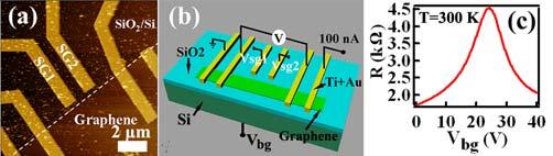
2 Graphene, composed of a two-dimensional (2D) hexagonal carbon lattice, stands out as a potential candidate for nanoelectronics and devices applications. 1-3 Its unusual band structure has a linear energy-momentum relation near the Dirac point where the valence and conduction bands meet, making graphene a zero-gap semiconductor. Both the type (electron or hole) and density of carriers in graphene can be easily controlled by using an electric field. Such an ambipolar electric field effect underlies a large number of work on graphene studying its electronic transport 4-7 as well as sensing 8,9 and other device-related applications The simplest and most common graphene field effect transistors (GFET) employ a heavily doped Si substrate as a global back gate. Such a global back gate tunes all the devices on the same substrate. In order to control individual GFETs (required in integrated circuits) and to realize more complex graphene devices, local gating using either top gates or side gates is required For example, top gates have been used to realize graphene-based bipolar devices (such as p-n junctions) within a single sheet. 14,16,17 However, deposition of dielectric required in the top gate fabrication could potentially lead to degradation of graphene mobility, and care must be taken and only very recently progresses have been made to overcome the detrimental effect Molitor et al. and Li et al. reported using graphene as side gates fabricated by reactive ion 15 and oxygen plasma etching 18, respectively. While capable to realize lateral modulation of charge density, this approach is limited by the size of graphene and the etching process can also degrade the graphene quality. Therefore, developing an easy and clean way of local gating on graphene is still desirable. Graf et al. gated a mesoscopic graphite wire 24 using metal side gates, with only limited efficacy due to the relative thickness of the graphite. In this work, we demonstrate ambipolar graphene field effect transistors (GFET) individually gated by local metal side gates, and investigate and analyze the widely tunable field effect transport in such graphene nanodevices. Our graphene samples are prepared by micromechanical exfoliation of graphite on top of 300 nm SiO 2 on heavily doped p-type (p ++ ) Si substrate. 25 Monolayer graphene can be identified by its optical contrast 25 and distinctive Raman spectrum 26. Metal side gates and contacts electrodes (5nm Ti+30nm Au) are fabricated in a one-step process 2
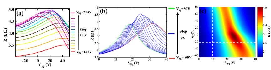
3 using e-beam lithography, metal deposition, and lift-off. No gate dielectric deposition or etching of graphene is needed in the process. Figure 1a shows the atomic force microscopy (AFM) image of a representative GFET device with two metal side gates (device 1 ). The typical distance between the side gate electrodes and edge of graphene ranges from several tens to hundreds of nanometers and is ~370nm for this device. A smaller distance gives stronger capacitive coupling between the side gate and graphene. Figure 1b shows the 3D schematic structure of the device and the corresponding circuits used in the measurements. All resistance measurements (4-terminals, see Fig. 1b) are performed at room temperature and in vacuum (<6 mtorr) by lock-in detection with a driving current of 100 na. All the gate voltages are applied by DC source meters. Figure 1d shows the room temperature back gate field effect for device 1. A characteristic ambipolar field effect is observed with a global Dirac point (V DP ) at 24V. The positive V DP indicates p-type doping, probably due to polymethyl methacrylate (PMMA) residue or adsorption of molecules (such as water) on the graphene surface. Our fabricated graphene devices have typical carrier mobilities of ~ cm 2 /Vs extracted from both Hall effect and back-gated field effect measurements. We have investigated the field effect controlled by both side and back gates. Data measured in device 1 are presented in Fig. 2. For simplicity, only one of the side gates (SG1, Fig. 1a) is used (using SG2 gives similar results). Figure 2a shows the resistance (R) as a function of the side gate voltage (V sg ) at a series of back gate voltages (V bg ) varied from 14.2V to 25.4V with a step of 0.8V. When the V bg =14.2V (much lower than V DP =24V, and the entire graphene being heavily p-type), R increases with the increasing V sg within the measurement range. When the V bg ~15.8V, a clear side gate Dirac point (V SDP ) with maximal R appears around 40V. Upon further increasing V bg, V SDP decreases (from positive toward negative) while the maximal R of the device increases till V bg reaches ~21.4V then decreases again. These results show that the side-gated field effect can be tuned by the back gate. We have also studied tuning of the back gated field effect for this device by the side gate, by measuring R as a function of V bg at various V sg (Fig. 2b). We observe similar as in Fig. 2a, that is, the back-gate 3
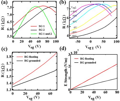
4 charge neutral point (V DP ) of the device continuously decreases as V sg increases (from -60 to 80V), while the R maximum in the V bg sweep first increases then decreases (reaching a peak at V sg ~7.5V). Figure 2c shows the 2D color-scale plot of R as a function of both V bg and V sg. The vertical and horizontal cuts in such a color plot correspond to similar side-gated and back-gated field effect curves shown in Fig. 2a and 2b respectively. The color plot (Fig. 2c) clearly shows the shift of side/back gated field effect as controlled by the back/side gate, as well as a global maximum in resistance as V sg ~0V and V bg ~25V. Qualitatively similar tuning of back and side gated field effect were previously demonstrated with graphene side gates. 15 We have also investigated the field effect due to the side gate only and how it may be affected by another side gate as shown in Fig. 3a and b. An ambipolar field effect is observed by sweeping the side gate voltage only. In Fig. 3a, all of the curves show clear side gate Dirac points. For SG1, V SDP1 ~ 70V, which is lower than V SDP2 ~90V. This difference may be due to the better capacitive coupling between SG1 and graphene or the charge inhomogeneity in the graphene. 27 When both side gates are used simultaneously, the joint field effect has a further reduced V SDP ~50V. Furthermore, we find that the side-gated field effect due to SG1 can be continuously tuned by applying a voltage to SG2 (V sg2 ) as shown in Fig. 3b. Increasing V sg2 from -80V to 80V tunes the field effect due to SG1 from p-type behavior (R increases with increasing V sg2 within the measurement range) to ambipolar, with V SDP1 decreasing from positive to 0V and even to negative (Fig. 3b). Similar results are also obtained when we sweep V sg2 at various V sg1. The on/off resistance modulation ratio of side-gated field effect can reach ~2 and become comparable to that of back gated field effect (Fig. 1c). The limited on/off ratio from side gated graphene FET may be related to the charge inhomogeneity 23, 28 induced by the non-uniform electric field from the side gate. We have also observed that the side-gated field effect is sensitive to the electrical grounding of the back gate. This is demonstrated in Fig. 3c, with measurements performed on a device 2 with only one local metal side gate but otherwise similar to 4
5 device 1. It can be seen that the side-gated field effect with the back gate floating is much stronger than the case with the back gate grounded. We have performed finite element (COMSOL Multiphysics 3.5a) simulations to calculate the spatial electric field profile with various gate configurations. Figure 3d shows the calculated electric field strength at a representative point above graphene as a function of V sg for the two different back gate conditions. It can be seen that the electric field at graphene is stronger with a floating back gate (than a grounded back gate), leading to the stronger field effect observed (Fig. 3c). In summary, we have demonstrated metal-side-gated ambipolar graphene field effect transistors, fabricated in a one-step process without any gate dielectric deposition or graphene etching. The local metal side gates show promising ability to tune the field effect in graphene and can be used to control individual graphene nanodevices, with many potential applications in carbon-based electronics. We thank Miller Family Endowment, Midwest Institute for Nanoelectronics Discovery (MIND), Indiana Economic Development Corporation (IEDC), NSF (ECCS ), DHS and DTRA for partial support of this research. 5
6 References: 1 A. K. Geim and K. S. Novoselov, Nature Mater. 6, 183 (2007). 2 A. K. Geim, Science 324, 1530 (2009). 3 C. Berger, Z. Song, X. Li, X. Wu, N. Brown, C. Naud, D. Mayou, T. Li, J. Hass, A. N. Marchenkov, E. H. Conrad, P. N. First, and W. A. de Heer, Science 312, 1191 (2006). 4 K. S. Novoselov, A. K. Geim, S. V. Morozov, D. Jiang, M. I. Katsnelson, I. V. Grigorieva, S. V. Dubonos, and A. A. Firsov, Nature (London) 438, 197 (2005). 5 Y. Zhang, Y.W. Tan, H. L. Stormer, and P. Kim, Nature (London) 438, 201 (2005). 6 K. I. Bolotin, F. Ghahari, M. D. Shulman, H. L. Stormer, and P. Kim, Nature 462, 196 (2009). 7 X. Du, I. Skachko, F. Duerr, A. Luican, and E. Y. Andrei, Nature 462, 192 (2009). 8 F. Schedin, A. K. Geim, S. V. Morozov, D. Jiang, E. H. Hill, P. Blake, and K. S. Novoselov, Nature Mater. 6, 652 (2007). 9 S. Pisana, P. M. Braganca, E. E. Marinero, and B. A Gurney, Nano Lett. 10, 341 (2010). 10 H. Wang, D. Nezich, J. Kong, and T. Palacios, IEEE Electron Device Lett. 30, 547 (2009). 11 M. Y. Han, B. Oezyilmaz, Y. Zhang, and P. Kim, Phys. Rev. Lett. 98, (2007). 12 Z. Chen, Y. -M. Lin, M. J. Rooks, and P. Avouris, Physica E 40, 228 (2007). 13 M. C. Lemme, T. J. Echtermeyer, M. Baus, and H. Kurz, IEEE Electron Device Lett. 28, 283 (2007). 6
7 14 J. R. Williams, L. DiCarlo, and C. M. Marcus, Science 317, 638 (2007). 15 F. Molitor, J. Guttinger, C. Stampfer, D. Graf, T. Ihn, and K. Ensslin, Phys. Rev. B 76, (2007). 16 B. Huard, J. A. Sulpizio, N. Stander, K. Todd, B. Yang, and D. Goldhaber-Gordon, Phys. Rev. Lett. 98, (2007). 17 B. Ozyilmaz, P. Jarillo-Herrero, D. Efetov, D. A. Abanin, L. S. Levitov, and P. Kim, Phys. Rev. Lett. 99, (2007). 18 X. Li, X. Wu, M. Sprinkle, F. Ming, M. Ruan, Y. Hu, C. Berger, and W. A. de Heer, Phys. Status Solidi A 207, 286 (2010). 19 K. Zou, X. Hong, D. Keefer, and J. Zhu, arxiv: v2 (2009). 20 D. B. Farmer, H. -Y Chiu, Y. -M Lin, K. A. Jenkins, F. Xia, and P. Avouris, Nano Lett. 9, 4474 (2009). 21 T. Shen, J. J. Gu, M. Xu, Y. Q. Wu, M. L. Bolen, M. A. Capano, L. W. Engel, and P. D. Ye, Appl. Phys. Lett. 95, (2009). 22 G. Liu, J. Velasco, W. Bao, and C.N. Lau, Appl. Phys. Lett. 92, (2008). 23 J. S. Moon, D. Curtis, S. Bui, M. Hu, D. K. Gaskill, J. L. Tedesco, P. Asbeck, G. G. Jernigan, B. L. VanMil, R. L. Myers-Ward, C. R. Eddy, Jr., P. M. Campbell, and X. Weng, IEEE Electron Device Lett. 31, 260 (2010). 24 D. Graf, F. Molitor, T. Ihn, and K. Ensslin, Phys Rev. B (2007). 25 K. S. Novoselov, A. K. Geim, S. V. Morozov, D. Jiang, Y. Zhang, S. V. Dubonos, I. V. Grigorieva, and A. A. Firsov, Science (2004). 26 A. C. Ferrari, Solid State Commun. 143, 47 (2007). 27 P. Blake, R. Wang, S. V. Morozov, F. Schedin, L. A. Ponomarenko, A. A. Zhukov, R. R. Nair, I. V. Grigorieva, K. S. Novoselov, and A. K. Geim, Solid State Commun. 149, 1068 (2009). 7
8 28 I. Meric, M. Y. Han, A. F. Young, B. Ozyilmaz, P. Kim, and K. L. Sheppard, Nat. Nanotechnol. 3, 654 (2008). Figure captions: FIG. 1. (a) AFM image of a graphene FET (device 1 ) with two local metal side gates ( SG1 and SG2 ). The dash line marks the edge of graphene, separated by ~370 nm from the side gates for this device. (b) The 3D schematic of the device and corresponding circuits used in the measurements. (c) The global field effect of device 1 by sweeping the back gate voltage. The FET mobility of this device is ~ 3500 cm 2 /Vs. FIG. 2. (a) Resistance (R) of the graphene device as a function of side gate voltage (V sg ) at various back gate voltages (V bg ). (b) R as a function of V bg at various V sg. (c) Two-dimensional (2D) color plot of R as a function of V bg and V sg. Curves in (a) and (b) correspond to vertical and horizontal line cuts in the color plot. All data measured in device 1 using SG1 as the side gate (Fig.1). FIG. 3. (a) Field effect controlled by one or two side gates (device 1 ). (b) R of device 1 as a function of V sg1 at various V sg2. (c) The side gated field effect measured in another device 2 (similar to device 1, but with one side gate only) with back gate grounded or floating respectively. (d) Calculated electric field strength (by COMSOL, for a device structure similar to that of device 2 ) at a representative point (1 nm above graphene and 250 nm from the left edge) as a function of V sg at different back gate conditions. 8
9 9
10 10
Non-volatile switching in graphene field effect devices. Abstract
 Non-volatile switching in graphene field effect devices T.J. Echtermeyer a1, M.C. Lemme a, M. Baus a, B.N. Szafranek a, A.K. Geim b, H. Kurz a a Advanced Microelectronic Center Aachen (AMICA), AMO GmbH,
Etching of Graphene Devices with a Helium Ion Beam
 Etching of Graphene Devices with a Helium Ion Beam The Harvard community has made this article openly available. Please share how this access benefits you. Your story matters Citation Lemme, Max C., David
Transport Properties of Graphene Nanoribbon Transistors on. Chemical-Vapor-Deposition Grown Wafer-Scale Graphene
 Transport Properties of Graphene Nanoribbon Transistors on Chemical-Vapor-Deposition Grown Wafer-Scale Graphene Wan Sik Hwang 1, a), Kristof Tahy 1, Xuesong Li 2, Huili (Grace) Xing 1, Alan C. Seabaugh
Tunneling characteristics of graphene
 Tunneling characteristics of graphene Young Jun Shin, 1,2 Gopinadhan Kalon, 1,2 Jaesung Son, 1 Jae Hyun Kwon, 1,2 Jing Niu, 1 Charanjit S. Bhatia, 1 Gengchiau Liang, 1 and Hyunsoo Yang 1,2,a) 1 Department
Ambipolar bistable switching effect of graphene
 Ambipolar bistable switching effect of graphene Young Jun Shin, 1,2 Jae Hyun Kwon, 1,2 Gopinadhan Kalon, 1,2 Kai-Tak Lam, 1 Charanjit S. Bhatia, 1 Gengchiau Liang, 1 and Hyunsoo Yang 1,2,a) 1 Department
Intrinsic Electronic Transport Properties of High. Information
 Intrinsic Electronic Transport Properties of High Quality and MoS 2 : Supporting Information Britton W. H. Baugher, Hugh O. H. Churchill, Yafang Yang, and Pablo Jarillo-Herrero Department of Physics, Massachusetts
Molecular Dynamics Study of Thermal Rectification in Graphene Nanoribbons
 Molecular Dynamics Study of Thermal Rectification in Graphene Nanoribbons Jiuning Hu 1* Xiulin Ruan 2 Yong P. Chen 3# 1School of Electrical and Computer Engineering and Birck Nanotechnology Center, Purdue
Molecular Dynamics Study of Thermal Rectification in Graphene Nanoribbons
 Int J Thermophys (2012) 33:986 991 DOI 10.1007/s10765-012-1216-y Molecular Dynamics Study of Thermal Rectification in Graphene Nanoribbons Jiuning Hu Xiulin Ruan Yong P. Chen Received: 26 June 2009 / Accepted:
Effect of electron-beam irradiation on graphene field effect devices
 Effect of electron-beam irradiation on graphene field effect devices Isaac Childres 1,2, Luis A. Jauregui 2,3, Mike Foxe 4,#, Jifa Tian 1,2, Romaneh Jalilian 1,2,*, Igor Jovanovic 4,#, Yong P. Chen 1,2,3,$
Raman Imaging and Electronic Properties of Graphene
 Raman Imaging and Electronic Properties of Graphene F. Molitor, D. Graf, C. Stampfer, T. Ihn, and K. Ensslin Laboratory for Solid State Physics, ETH Zurich, 8093 Zurich, Switzerland ensslin@phys.ethz.ch
High-Quality BN-Graphene-BN Nanoribbon Capacitors Modulated by Graphene Side-gate Electrodes
 High-Quality BN-Graphene-BN Nanoribbon Capacitors Modulated by Graphene Side-gate Electrodes Yang Wang, Xiaolong Chen, Weiguang Ye, Zefei Wu, Yu Han, Tianyi Han, Yuheng He, Yuan Cai and Ning Wang* Department
The role of charge traps in inducing hysteresis: capacitance voltage measurements on top gated bilayer graphene
 The role of charge traps in inducing hysteresis: capacitance voltage measurements on top gated bilayer graphene Gopinadhan Kalon, Young Jun Shin, Viet Giang Truong, Alan Kalitsov, and Hyunsoo Yang a) Department
Quantum transport through graphene nanostructures
 Quantum transport through graphene nanostructures S. Rotter, F. Libisch, L. Wirtz, C. Stampfer, F. Aigner, I. Březinová, and J. Burgdörfer Institute for Theoretical Physics/E136 December 9, 2009 Graphene
From One Electron to One Hole: Quasiparticle Counting in Graphene Quantum Dots Determined by Electrochemical and Plasma Etching
 From One Electron to One Hole: Quasiparticle Counting in Graphene Quantum Dots Determined by Electrochemical and Plasma Etching S. Neubeck 1, L. A. Ponomarenko 1, F. Freitag 1, A. J. M. Giesbers 2, U.
Precision Cutting and Patterning of Graphene with Helium Ions. 1.School of Engineering and Applied Sciences, Harvard University, Cambridge MA 02138
 Precision Cutting and Patterning of Graphene with Helium Ions D.C. Bell 1,2, M.C. Lemme 3, L. A. Stern 4, J.R. Williams 1,3, C. M. Marcus 3 1.School of Engineering and Applied Sciences, Harvard University,
TRANSVERSE SPIN TRANSPORT IN GRAPHENE
 International Journal of Modern Physics B Vol. 23, Nos. 12 & 13 (2009) 2641 2646 World Scientific Publishing Company TRANSVERSE SPIN TRANSPORT IN GRAPHENE TARIQ M. G. MOHIUDDIN, A. A. ZHUKOV, D. C. ELIAS,
Reduction of Fermi velocity in folded graphene observed by resonance Raman spectroscopy
 Reduction of Fermi velocity in folded graphene observed by resonance Raman spectroscopy Zhenhua Ni, Yingying Wang, Ting Yu, Yumeng You, and Zexiang Shen* Division of Physics and Applied Physics, School
Graphene Transistors Fabricated via Transfer-Printing In Device Active-Areas on Large Wafer
 Graphene Transistors Fabricated via Transfer-Printing In Device Active-Areas on Large Wafer NANO LETTERS 2007 Vol. 7, No. 12 3840-3844 Xiaogan Liang, Zengli Fu, and Stephen Y. Chou* NanoStructure Laboratory,
Hybrid Surface-Phonon-Plasmon Polariton Modes in Graphene /
 Supplementary Information: Hybrid Surface-Phonon-Plasmon Polariton Modes in Graphene / Monolayer h-bn stacks Victor W. Brar 1,2, Min Seok Jang 3,, Michelle Sherrott 1, Seyoon Kim 1, Josue J. Lopez 1, Laura
RF Performance Projections of Graphene FETs vs. Silicon MOSFETs
 1 RF Performance Projections of Graphene FETs vs. Silicon MOSFETs S. Rodriguez *, S. Vaziri *, M. Ostling *, A. Rusu *, E. Alarcon *,#, M.C. Lemme *1 * KTH Royal Institute of Technology, School of ICT,
ICTP Conference Graphene Week 2008
 1960-3 ICTP Conference Graphene Week 2008 25-29 August 2008 Current-induced cleaning of graphene J. Moser CIN2 Barcelona, Campus UAB, Bellaterra, Spain A. Barreiro CIN2 Barcelona, Campus UAB, Bellaterra,
Supplementary Information for
 Supplementary Information for Highly Stable, Dual-Gated MoS 2 Transistors Encapsulated by Hexagonal Boron Nitride with Gate-Controllable Contact Resistance and Threshold Voltage Gwan-Hyoung Lee, Xu Cui,
arxiv: v1 [cond-mat.mes-hall] 22 Dec 2011
![arxiv: v1 [cond-mat.mes-hall] 22 Dec 2011](/thumbs/76/73542175.jpg "arxiv: v1 [cond-mat.mes-hall] 22 Dec 2011") Direct Measurement of the Fermi Energy in Graphene Using a Double Layer Structure Seyoung Kim, 1 Insun Jo, 2 D. C. Dillen, 1 D. A. Ferrer, 1 B. Fallahazad, 1 Z. Yao, 2 S. K. Banerjee, 1 and E. Tutuc 1
Direct Measurement of the Fermi Energy in Graphene Using a Double Layer Structure Seyoung Kim, 1 Insun Jo, 2 D. C. Dillen, 1 D. A. Ferrer, 1 B. Fallahazad, 1 Z. Yao, 2 S. K. Banerjee, 1 and E. Tutuc 1
crystals were phase-pure as determined by x-ray diffraction. Atomically thin MoS 2 flakes were
 Nano Letters (214) Supplementary Information for High Mobility WSe 2 p- and n-type Field Effect Transistors Contacted by Highly Doped Graphene for Low-Resistance Contacts Hsun-Jen Chuang, Xuebin Tan, Nirmal
Edge chirality determination of graphene by Raman spectroscopy
 Edge chirality determination of graphene by Raman spectroscopy YuMeng You, ZhenHua Ni, Ting Yu, ZeXiang Shen a) Division of Physics and Applied Physics, School of Physical and Mathematical Sciences, Nanyang
Highly Conductive 3D Nano-Carbon: Stacked Multilayer Graphene System with Interlayer Decoupling
 Highly Conductive 3D Nano-Carbon: Stacked Multilayer Graphene System with Interlayer Decoupling Tianhua Yu, Changdong Kim, and Bin Yu*, College of Nanoscale Science and Engineering, State University of
Mobility in Graphene Double Gate Field Effect Transistors
 This work has been published in Solid State Electronics, Vol. 52. Issue 4, pp. 514-518, 2008. Mobility in Graphene Double Gate Field Effect Transistors M.C. Lemme *, T.J. Echtermeyer, M. Baus, B.N. Szafranek,
Understanding the effect of n-type and p-type doping in the channel of graphene nanoribbon transistor
 Bull. Mater. Sci., Vol. 39, No. 5, September 2016, pp. 1303 1309. DOI 10.1007/s12034-016-1277-9 c Indian Academy of Sciences. Understanding the effect of n-type and p-type doping in the channel of graphene
Electron Beam Nanosculpting of Suspended Graphene Sheets
 Electron Beam Nanosculpting of Suspended Graphene Sheets Michael D. Fischbein and Marija Drndić Department of Physics and Astronomy, University of Pennsylvania, Philadelphia, PA 19104 We demonstrate high-resolution
Raman spectroscopy of graphene on different substrates and influence of defects
 Bull. Mater. Sci., Vol. 31, No. 3, June 2008, pp. 579 584. Indian Academy of Sciences. Raman spectroscopy of graphene on different substrates and influence of defects ANINDYA DAS, BISWANATH CHAKRABORTY
AN IMPROVED METHOD FOR TRANSFERRING GRAPHENE GROWN BY CHEMICAL VAPOR DEPOSITION
 NANO: Brief Reports and Reviews Vol. 7, No. 1 (2012) 1150001 (6 pages) World Scienti c Publishing Company DOI: 10.1142/S1793292011500019 AN IMPROVED METHOD FOR TRANSFERRING GRAPHENE GROWN BY CHEMICAL VAPOR
Tunable Graphene Single Electron Transistor
 Tunable Graphene Single Electron Transistor NANO LETTERS 2008 Vol. 8, No. 8 2378-2383 C. Stampfer,* E. Schurtenberger, F. Molitor, J. Güttinger, T. Ihn, and K. Ensslin Solid State Physics Laboratory, ETH
A. Optimizing the growth conditions of large-scale graphene films
 1 A. Optimizing the growth conditions of large-scale graphene films Figure S1. Optical microscope images of graphene films transferred on 300 nm SiO 2 /Si substrates. a, Images of the graphene films grown
Lithography-free Fabrication of High Quality Substrate-supported and. Freestanding Graphene devices
 Lithography-free Fabrication of High Quality Substrate-supported and Freestanding Graphene devices W. Bao 1, G. Liu 1, Z. Zhao 1, H. Zhang 1, D. Yan 2, A. Deshpande 3, B.J. LeRoy 3 and C.N. Lau 1, * 1
Supporting Online Material for
 www.sciencemag.org/cgi/content/full/327/5966/662/dc Supporting Online Material for 00-GHz Transistors from Wafer-Scale Epitaxial Graphene Y.-M. Lin,* C. Dimitrakopoulos, K. A. Jenkins, D. B. Farmer, H.-Y.
Understanding the Electrical Impact of Edge Contacts in Few-Layer Graphene
 Purdue University Purdue e-pubs Birck and NCN Publications Birck Nanotechnology Center 4-2014 Understanding the Electrical Impact of Edge Contacts in Few-Layer Graphene Tao Chu Purdue University, Birck
state spectroscopy Xing Lan Liu, Dorothee Hug, Lieven M. K. Vandersypen Netherlands
 Gate-defined graphene double quantum dot and excited state spectroscopy Xing Lan Liu, Dorothee Hug, Lieven M. K. Vandersypen Kavli Institute of Nanoscience, Delft University of Technology, P.O. Box 5046,
Atomic-Layer-Deposited High-k Dielectric Integration on Epitaxial Graphene. P.D. Ye, A.T. Neal, T. Shen, J.J. Gu, M.L. Bolen, and M. A.
 459 10.1149/1.3481634 The Electrochemical Society Atomic-Layer-Deposited High-k Dielectric Integration on Epitaxial Graphene P.D. Ye, A.T. Neal, T. Shen, J.J. Gu, M.L. Bolen, and M. A. Capano School of
Supporting Information. by Hexagonal Boron Nitride
 Supporting Information High Velocity Saturation in Graphene Encapsulated by Hexagonal Boron Nitride Megan A. Yamoah 1,2,, Wenmin Yang 1,3, Eric Pop 4,5,6, David Goldhaber-Gordon 1 * 1 Department of Physics,
arxiv: v1 [cond-mat.mtrl-sci] 29 Jan 2008
![arxiv: v1 [cond-mat.mtrl-sci] 29 Jan 2008](/thumbs/85/92280048.jpg "arxiv: v1 [cond-mat.mtrl-sci] 29 Jan 2008") Strong Suppression of Electrical Noise in Bilayer Graphene Nano Devices YU-MING LIN and PHAEDON AVOURIS IBM T. J. Watson Research Center, arxiv:0801.4576v1 [cond-mat.mtrl-sci] 29 Jan 2008 Yorktown Heights,
Strong Suppression of Electrical Noise in Bilayer Graphene Nano Devices YU-MING LIN and PHAEDON AVOURIS IBM T. J. Watson Research Center, arxiv:0801.4576v1 [cond-mat.mtrl-sci] 29 Jan 2008 Yorktown Heights,
Gate-defined graphene double quantum dot and excited state spectroscopy
 pubs.acs.org/nanolett Gate-defined graphene double quantum dot and excited state spectroscopy Xing Lan Liu,* Dorothee Hug, and Lieven M. K. Vandersypen Kavli Institute of Nanoscience, Delft University
Sub-5 nm Patterning and Applications by Nanoimprint Lithography and Helium Ion Beam Lithography
 Sub-5 nm Patterning and Applications by Nanoimprint Lithography and Helium Ion Beam Lithography Yuanrui Li 1, Ahmed Abbas 1, Yuhan Yao 1, Yifei Wang 1, Wen-Di Li 2, Chongwu Zhou 1 and Wei Wu 1* 1 Department
Other Hydrocarbon Sources
 Chemical Vapor Deposition Growth of Graphene using Other Hydrocarbon Sources Zhancheng Li, Ping Wu, Chenxi Wang, Xiaodong Fan, Wenhua Zhang, Xiaofang Zhai, Changgan Zeng,* Zhenyu Li,* Jinlong Yang, and
Graphene Thickness Determination Using Reflection and Contrast Spectroscopy
 Graphene Thickness Determination Using Reflection and Contrast Spectroscopy NANO LETTERS 2007 Vol. 7, No. 9 2758-2763 Z. H. Ni, H. M. Wang, J. Kasim, H. M. Fan,, T. Yu, Y. H. Wu, Y. P. Feng, and Z. X.
Supporting Online Material for
 www.sciencemag.org/cgi/content/full/320/5874/356/dc1 Supporting Online Material for Chaotic Dirac Billiard in Graphene Quantum Dots L. A. Ponomarenko, F. Schedin, M. I. Katsnelson, R. Yang, E. W. Hill,
Multicolor Graphene Nanoribbon/Semiconductor Nanowire. Heterojunction Light-Emitting Diodes
 Multicolor Graphene Nanoribbon/Semiconductor Nanowire Heterojunction Light-Emitting Diodes Yu Ye, a Lin Gan, b Lun Dai, *a Hu Meng, a Feng Wei, a Yu Dai, a Zujin Shi, b Bin Yu, a Xuefeng Guo, b and Guogang
Lithography-Free Fabrication of High Quality Substrate- Supported and Freestanding Graphene Devices
 98 DOI 10.1007/s12274-010-1013-5 Research Article Lithography-Free Fabrication of High Quality Substrate- Supported and Freestanding Graphene Devices Wenzhong Bao 1, Gang Liu 1, Zeng Zhao 1, Hang Zhang
Supporting Information Available:
 Supporting Information Available: Photoresponsive and Gas Sensing Field-Effect Transistors based on Multilayer WS 2 Nanoflakes Nengjie Huo 1, Shengxue Yang 1, Zhongming Wei 2, Shu-Shen Li 1, Jian-Bai Xia
Quantum transport through graphene nanostructures
 Quantum transport through graphene nanostructures F. Libisch, S. Rotter, and J. Burgdörfer Institute for Theoretical Physics/E136, January 14, 2011 Graphene [1, 2], the rst true two-dimensional (2D) solid,
The role of contacts in graphene transistors: A scanning photocurrent study
 The role of contacts in graphene transistors: A scanning photocurrent study T. Mueller*, F. Xia, M. Freitag, J. Tsang, and Ph. Avouris* Email: tmuelle@us.ibm.com, avouris@us.ibm.com www.research.ibm.com/nanoscience
Supplementary Figure S1. AFM images of GraNRs grown with standard growth process. Each of these pictures show GraNRs prepared independently,
 Supplementary Figure S1. AFM images of GraNRs grown with standard growth process. Each of these pictures show GraNRs prepared independently, suggesting that the results is reproducible. Supplementary Figure
Fabrication of graphene nanogap with crystallographically matching edges and its. electron emission properties
 Fabrication of graphene nanogap with crystallographically matching edges and its electron emission properties H. M. Wang, 1 Z. Zheng, 1 Y.Y.Wang, 1 J.J. Qiu, Z.B. Guo, Z. X. Shen, 1 and T. Yu 1,* 1 Division
Solvothermal Reduction of Chemically Exfoliated Graphene Sheets
 Solvothermal Reduction of Chemically Exfoliated Graphene Sheets Hailiang Wang, Joshua Tucker Robinson, Xiaolin Li, and Hongjie Dai* Department of Chemistry and Laboratory for Advanced Materials, Stanford
High Mobility Ambipolar MoS 2 Field-Effect Transistors: Substrate and Dielectric Effects
 High Mobility Ambipolar MoS 2 Field-Effect Transistors: Substrate and Dielectric Effects Wenzhong Bao, Xinghan Cai, Dohun Kim, Karthik Sridhara, and Michael S. Fuhrer Center for Nanophysics and Advanced
NiCl2 Solution concentration. Etching Duration. Aspect ratio. Experiment Atmosphere Temperature. Length(µm) Width (nm) Ar:H2=9:1, 150Pa
 Width (nm) Ar:H2=9:1, 150Pa") Experiment Atmosphere Temperature #1 # 2 # 3 # 4 # 5 # 6 # 7 # 8 # 9 # 10 Ar:H2=9:1, 150Pa Ar:H2=9:1, 150Pa Ar:H2=9:1, 150Pa Ar:H2=9:1, 150Pa Ar:H2=9:1, 150Pa Ar:H2=9:1, 150Pa Ar:H2=9:1, 150Pa Ar:H2=9:1,
Experiment Atmosphere Temperature #1 # 2 # 3 # 4 # 5 # 6 # 7 # 8 # 9 # 10 Ar:H2=9:1, 150Pa Ar:H2=9:1, 150Pa Ar:H2=9:1, 150Pa Ar:H2=9:1, 150Pa Ar:H2=9:1, 150Pa Ar:H2=9:1, 150Pa Ar:H2=9:1, 150Pa Ar:H2=9:1,
Low-temperature ballistic transport in nanoscale epitaxial graphene cross junctions
 Low-temperature ballistic transport in nanoscale epitaxial graphene cross junctions S. Weingart, C. Bock, and U. Kunze Werkstoffe und Nanoelektronik, Ruhr-Universität Bochum, D-44780 Bochum, Germany F.
A Graphene Quantum Dot with a Single Electron
 A Graphene Quantum Dot with a Single Electron Transistor as Integrated Charge Sensor Ling-Jun Wang, Gang Cao, Tao Tu, Hai-Ou Li, Cheng Zhou, Xiao-Jie Hao, Zhan Su, Guang- Can Guo, Guo-Ping Guo *, and Hong-Wen
Transport properties through double-magnetic-barrier structures in graphene
 Chin. Phys. B Vol. 20, No. 7 (20) 077305 Transport properties through double-magnetic-barrier structures in graphene Wang Su-Xin( ) a)b), Li Zhi-Wen( ) a)b), Liu Jian-Jun( ) c), and Li Yu-Xian( ) c) a)
Efficient Preparation of Large-Area Graphene Oxide Sheets for Transparent Conductive Films
 Supporting Information Efficient Preparation of Large-Area Graphene Oxide Sheets for Transparent Conductive Films Jinping Zhao, Songfeng Pei, Wencai Ren*, Libo Gao and Hui-Ming Cheng* Shenyang National
Graphene devices and integration: A primer on challenges
 Graphene devices and integration: A primer on challenges Archana Venugopal (TI) 8 Nov 2016 Acknowledgments: Luigi Colombo (TI) UT Dallas and UT Austin 1 Outline Where we are Issues o Contact resistance
Electronic Doping and Scattering by Transition Metals on Graphene
 Electronic Doping and Scattering by Transition Metals on Graphene K. Pi,* K. M. McCreary,* W. Bao, Wei Han, Y. F. Chiang, Yan Li, S.-W. Tsai, C. N. Lau, and R. K. Kawakami Department of Physics and Astronomy,
Local Growth of Graphene by Ion Implantation of Carbon in a Nickel Thin Film followed by Rapid Thermal Annealing
 Local Growth of Graphene by Ion Implantation of Carbon in a Nickel Thin Film followed by Rapid Thermal Annealing Jeong Hun Mun, Sung Kyu Lim and Byung Jin Cho J. Electrochem. Soc. 2012, Volume 159, Issue
Electrical transport in high-quality graphene pnp junctions
 Electrical transport in high-quality graphene pnp junctions To cite this article: Jairo Velasco Jr et al 2009 New J. Phys. 11 095008 View the article online for updates and enhancements. Related content
Soft Carrier Multiplication by Hot Electrons in Graphene
 Soft Carrier Multiplication by Hot Electrons in Graphene Anuj Girdhar 1,3 and J.P. Leburton 1,2,3 1) Department of Physics 2) Department of Electrical and Computer Engineering, and 3) Beckman Institute
Computational Model of Edge Effects in Graphene Nanoribbon Transistors
 Nano Res (2008) 1: 395 402 DOI 10.1007/s12274-008-8039-y Research Article 00395 Computational Model of Edge Effects in Graphene Nanoribbon Transistors Pei Zhao 1, Mihir Choudhury 2, Kartik Mohanram 2,
Polarization dependence of photocurrent in a metalgraphene-metal
 Polarization dependence of photocurrent in a metalgraphene-metal device Minjung Kim, 1 Ho Ang Yoon, 2 Seungwoo Woo, 1 Duhee Yoon, 1 Sang Wook Lee, 2 and Hyeonsik Cheong 1,a) 1 Department of Physics, Sogang
Wafer-scale epitaxial graphene growth on the Si-face of hexagonal SiC 0001 for high frequency transistors
 Wafer-scale epitaxial graphene growth on the Si-face of hexagonal SiC 0001 for high frequency transistors Christos Dimitrakopoulos, a Yu-Ming Lin, Alfred Grill, Damon B. Farmer, Marcus Freitag, Yanning
Quantum-Hall plateau-plateau transition in top-gated epitaxial graphene grown on SiC (0001) (Dated: November 15, 2011) Abstract
 (Dated: November 15, 2011) Abstract") Quantum-Hall plateau-plateau transition in top-gated epitaxial graphene grown on SiC (0001) T. Shen, 1,2 A.T. Neal, 1 M.L. Bolen, 1 J.J. Gu, 1 L.W. Engel, 3 M.A. Capano, 1 and P.D. Ye 1,* 1 Electrical
Quantum-Hall plateau-plateau transition in top-gated epitaxial graphene grown on SiC (0001) T. Shen, 1,2 A.T. Neal, 1 M.L. Bolen, 1 J.J. Gu, 1 L.W. Engel, 3 M.A. Capano, 1 and P.D. Ye 1,* 1 Electrical
Impact of Calcium on Transport Property of Graphene. Jyoti Katoch and Masa Ishigami*
 Impact of Calcium on Transport Property of Graphene Jyoti Katoch and Masa Ishigami* Department of Physics and Nanoscience Technology Center, University of Central Florida, Orlando, FL, 32816 *Corresponding
Supporting Information. Nanoscale control of rewriteable doping patterns in pristine graphene/boron nitride heterostructures
 Supporting Information Nanoscale control of rewriteable doping patterns in pristine graphene/boron nitride heterostructures Jairo Velasco Jr. 1,5,, Long Ju 1,, Dillon Wong 1,, Salman Kahn 1, Juwon Lee
HIGH-PERFORMANCE sensors for electromagnetic radiation
 IEEE TRANSACTIONS ON NANOTECHNOLOGY, VOL. 11, NO. 3, MAY 2012 581 Graphene Field-Effect Transistors on Undoped Semiconductor Substrates for Radiation Detection Michael Foxe, Student Member, IEEE, GabrielLopez,
arxiv: v1 [cond-mat.mes-hall] 27 Mar 2010
![arxiv: v1 [cond-mat.mes-hall] 27 Mar 2010](/thumbs/89/98385059.jpg "arxiv: v1 [cond-mat.mes-hall] 27 Mar 2010") Intrinsic Limits of Subthreshold Slope in Biased Bilayer arxiv:1003.5284v1 [cond-mat.mes-hall] 27 Mar 2010 Graphene Transistor Kausik Majumdar, Kota V. R. M. Murali, Navakanta Bhat and Yu-Ming Lin Department
Intrinsic Limits of Subthreshold Slope in Biased Bilayer arxiv:1003.5284v1 [cond-mat.mes-hall] 27 Mar 2010 Graphene Transistor Kausik Majumdar, Kota V. R. M. Murali, Navakanta Bhat and Yu-Ming Lin Department
Chun Ning Lau (Jeanie) Graphene Quantum Electronics: p-n Junctions and Atomic Switches
 Graphene Quantum Electronics: p-n Junctions and Atomic Switches") Chun Ning Lau (Jeanie) Graphene Quantum Electronics: p-n Junctions and Atomic Switches Acknowledgement Graduate Students Feng Miao Wenzhong Bao Discussion With Shan-Wan Tsai, Antonio Castro-Neto, Michael
Chun Ning Lau (Jeanie) Graphene Quantum Electronics: p-n Junctions and Atomic Switches Acknowledgement Graduate Students Feng Miao Wenzhong Bao Discussion With Shan-Wan Tsai, Antonio Castro-Neto, Michael
Towards electron transport measurements in chemically modified graphene: effect of a solvent
 Towards electron transport measurements in chemically modified graphene: effect of a solvent To cite this article: Arnhild Jacobsen et al 2010 New J. Phys. 12 125007 View the article online for updates
Record Maximum Oscillation Frequency in C-face Epitaxial Graphene Transistors
 Record Maximum Oscillation Frequency in C-face Epitaxial Graphene Transistors Zelei Guo 1, Rui Dong 1, Partha Sarathi Chakraborty 2, Nelson Lourenco 2, James Palmer 1, Yike Hu 1, Ming Ruan 1, John Hankinson
Spin Injection into a Graphene Thin Film at Room Temperature
 Spin Injection into a Graphene Thin Film at Room Temperature Megumi Ohishi, Masashi Shiraishi*, Ryo Nouchi, Takayuki Nozaki, Teruya Shinjo, and Yoshishige Suzuki Graduate School of Engineering Science,
Graphene Field Effect Transistor as Radiation Sensor
 2011 IEEE Nuclear Science Symposium Conference Record NPl.M-225 Graphene Field Effect Transistor as Radiation Sensor A. Patil, O. Koybasi, G. Lopez, Student Member, IEEE, M. Foxe, Student Member, IEEE,
Nonlinear optical conductance in a graphene pn junction in the terahertz regime
 University of Wollongong Research Online Faculty of Engineering - Papers (Archive) Faculty of Engineering and Information Sciences 2010 Nonlinear optical conductance in a graphene pn junction in the terahertz
Epitaxial Graphene Growth on SiC Wafers. Washington, DC 20375
 Epitaxial Graphene Growth on SiC Wafers D.K. Gaskill 1, G.G. Jernigan 2, P.M. Campbell 2, J.L. Tedesco 1, J.C. Culbertson 2, B.L. VanMil 1, R.L.Myers-Ward 1, C.R. Eddy, Jr. 1 J. Moon 3, D. Curtis 3, M.
Supplementary Figure 1. Selected area electron diffraction (SAED) of bilayer graphene and tblg. (a) AB
 of bilayer graphene and tblg. (a) AB") Supplementary Figure 1. Selected area electron diffraction (SAED) of bilayer graphene and tblg. (a) AB stacked bilayer graphene (b), (c), (d), (e), and (f) are twisted bilayer graphene with twist angle
Supplementary Figure 1. Selected area electron diffraction (SAED) of bilayer graphene and tblg. (a) AB stacked bilayer graphene (b), (c), (d), (e), and (f) are twisted bilayer graphene with twist angle
photonic crystals School of Space Science and Physics, Shandong University at Weihai, Weihai , China
 Enhanced absorption in heterostructures with graphene and truncated photonic crystals Yiping Liu 1, Lei Du 1, Yunyun Dai 2, Yuyu Xia 2, Guiqiang Du 1,* Guang Lu 1, Fen Liu 1, Lei Shi 2, Jian Zi 2 1 School
Graphene for Microwaves
 T hese days, electronics are moving toward faster, smaller, more efficient, yet cost effective, solutions. In doing so, the limits of what materials are currently available within the technologies are
Multilayer graphene under vertical electric field
 Multilayer graphene under vertical electric field S. Bala kumar and Jing Guo a) Department of Electrical and Computer Engineering, University of Florida, Gainesville, Florida 3608, USA Abstract We study
Monolayer Semiconductors
 Monolayer Semiconductors Gilbert Arias California State University San Bernardino University of Washington INT REU, 2013 Advisor: Xiaodong Xu (Dated: August 24, 2013) Abstract Silicon may be unable to
Device Performance Analysis of Graphene Nanoribbon Field-Effect Transistor with Rare- Earth Oxide (La 2 O 3 ) Based High-k Gate Dielectric
 Based High-k Gate Dielectric") Device Performance Analysis of Graphene Nanoribbon Field-Effect Transistor with Rare- Earth Oxide (La 2 O 3 ) Based High-k Gate Dielectric M. K. Bera 1, S. P. Pandey 2, A. K. Sharma 3, D. K. Tyagi 4, R.
Device Performance Analysis of Graphene Nanoribbon Field-Effect Transistor with Rare- Earth Oxide (La 2 O 3 ) Based High-k Gate Dielectric M. K. Bera 1, S. P. Pandey 2, A. K. Sharma 3, D. K. Tyagi 4, R.
Supporting Information
 Electronic Supplementary Material (ESI) for Nanoscale. This journal is The Royal Society of Chemistry 2016 Supporting Information Graphene transfer method 1 : Monolayer graphene was pre-deposited on both
Wafer-scale fabrication of graphene
 Wafer-scale fabrication of graphene Sten Vollebregt, MSc Delft University of Technology, Delft Institute of Mircosystems and Nanotechnology Delft University of Technology Challenge the future Delft University
MICROWAVE AND MILLIMETERWAVE ELECTRICAL PERMITTIVITY OF GRAPHENE MONOLAYER. G. Konstantinidis 3
 1 MICROWAVE AND MILLIMETERWAVE ELECTRICAL PERMITTIVITY OF GRAPHENE MONOLAYER Alina Cismaru 1, Mircea Dragoman 1*, Adrian Dinescu 1, Daniela Dragoman 2, G. Stavrinidis, G. Konstantinidis 3 1 National Institute
Chun Ning Lau (Jeanie) Graphene: Quantum Transport in a 2D Membrane
 Graphene: Quantum Transport in a 2D Membrane") Chun Ning Lau (Jeanie) Graphene: Quantum Transport in a 2D Membrane Grapheneʼs Double Identity Extraordinary Conductor 2D Elastic Membrane Novoselov et al Nature 2005; Zhang et al, Nature 2005. New model
Chun Ning Lau (Jeanie) Graphene: Quantum Transport in a 2D Membrane Grapheneʼs Double Identity Extraordinary Conductor 2D Elastic Membrane Novoselov et al Nature 2005; Zhang et al, Nature 2005. New model
Supplementary Figure 1 Dark-field optical images of as prepared PMMA-assisted transferred CVD graphene films on silicon substrates (a) and the one
 and the one") Supplementary Figure 1 Dark-field optical images of as prepared PMMA-assisted transferred CVD graphene films on silicon substrates (a) and the one after PBASE monolayer growth (b). 1 Supplementary Figure
Supplementary Figure 1 Dark-field optical images of as prepared PMMA-assisted transferred CVD graphene films on silicon substrates (a) and the one after PBASE monolayer growth (b). 1 Supplementary Figure
Fabrication and Electrical Characteristics of Graphene-based Charge-trap Memory Devices
 Journal of the Korean Physical Society, Vol. 61, No. 1, July 2012, pp. 108 112 Fabrication and Electrical Characteristics of Graphene-based Charge-trap Memory Devices Sejoon Lee Quantum-functional Semiconductor
SUPPLEMENTARY INFORMATION. Observation of tunable electrical bandgap in large-area twisted bilayer graphene synthesized by chemical vapor deposition
 SUPPLEMENTARY INFORMATION Observation of tunable electrical bandgap in large-area twisted bilayer graphene synthesized by chemical vapor deposition Jing-Bo Liu 1 *, Ping-Jian Li 1 *, Yuan-Fu Chen 1, Ze-Gao
Effect of oxygen plasma etching on graphene studied with Raman spectroscopy and electronic transport
 Effect of oxygen plasma etching on graphene studied with Raman spectroscopy and electronic transport Isaac Childres1,2, Luis A. Jauregui2,3, Jifa Tian1,2, Yong P. Chen1,2,3 1 Department of Physics, Purdue
Thickness Estimation of Epitaxial Graphene on SiC using Attenuation of Substrate Raman Intensity
 Thickness Estimation of Epitaxial Graphene on SiC using Attenuation of Substrate Raman Intensity Shriram Shivaraman 1, MVS Chandrashekhar 1, John J. Boeckl 2, Michael G. Spencer 1 1 School of Electrical
Klein tunneling in graphene p-n-p junctions
 10.1149/1.3569920 The Electrochemical Society Klein tunneling in graphene p-n-p junctions E. Rossi 1,J.H.Bardarson 2,3,P.W.Brouwer 4 1 Department of Physics, College of William and Mary, Williamsburg,
Supplementary Figure 1. Supplementary Figure 1 Characterization of another locally gated PN junction based on boron
 Supplementary Figure 1 Supplementary Figure 1 Characterization of another locally gated PN junction based on boron nitride and few-layer black phosphorus (device S1). (a) Optical micrograph of device S1.
Detection of Ionizing Radiations with Graphene Field Effect Transistors (GFET) Yong P. Chen Purdue University
 Yong P. Chen Purdue University") Detection of Ionizing Radiations with Graphene Field Effect Transistors (GFET) Yong P. Chen (yongchen@purdue.edu), Purdue University IEEE NSS 10/26/2009 Team Members: Isaac Childres, Mike Foxe, Gabriel
Detection of Ionizing Radiations with Graphene Field Effect Transistors (GFET) Yong P. Chen (yongchen@purdue.edu), Purdue University IEEE NSS 10/26/2009 Team Members: Isaac Childres, Mike Foxe, Gabriel
arxiv: v1 [cond-mat.mes-hall] 29 Nov 2013
![arxiv: v1 [cond-mat.mes-hall] 29 Nov 2013](/thumbs/74/71156913.jpg "arxiv: v1 [cond-mat.mes-hall] 29 Nov 2013") Transport Spectroscopy of a Graphene Quantum Dot Fabricated by Atomic Force Microscope Nanolithography R.K. Puddy, 1 C.J. Chua, 1 1,2, 3, and M.R. Buitelaar 1 Cavendish Laboratory, University of Cambridge,
Transport Spectroscopy of a Graphene Quantum Dot Fabricated by Atomic Force Microscope Nanolithography R.K. Puddy, 1 C.J. Chua, 1 1,2, 3, and M.R. Buitelaar 1 Cavendish Laboratory, University of Cambridge,
Scanning tunneling microscopy and spectroscopy of graphene layers on graphite
 Scanning tunneling microscopy and spectroscopy of graphene layers on graphite Adina Luican, Guohong Li and Eva Y. Andrei Department of Physics and Astronomy, Rutgers University, Piscataway, New Jersey
Supporting Information
 Supporting Information Monolithically Integrated Flexible Black Phosphorus Complementary Inverter Circuits Yuanda Liu, and Kah-Wee Ang* Department of Electrical and Computer Engineering National University