Optimal-enhanced Solar Cell Ultra-thinning with Broadband Nanophotonic Light Capture
|
|
|
- Dylan Sullivan
- 6 years ago
- Views:
Transcription

1 Accepted Manuscript Optimal-enhanced Solar Cell Ultra-thinning with Broadband Nanophotonic Light Capture Manuel J. Mendes, Sirazul Haque, Olalla Sanchez-Sobrado, Andreia Araújo, Hugo Águas, Elvira Fortunato, Rodrigo Martins PII: S (18) DOI: /j.isci Reference: ISCI 50 To appear in: ISCIENCE Received Date: 19 February 2018 Revised Date: 16 April 2018 Accepted Date: 24 April 2018 Please cite this article as: Mendes, M.J., Haque, S., Sanchez-Sobrado, O., Araújo, A., Águas, H., Fortunato, E., Martins, R., Optimal-enhanced Solar Cell Ultra-thinning with Broadband Nanophotonic Light Capture, ISCIENCE (2018), doi: /j.isci This is a PDF file of an unedited manuscript that has been accepted for publication. As a service to our customers we are providing this early version of the manuscript. The manuscript will undergo copyediting, typesetting, and review of the resulting proof before it is published in its final form. Please note that during the production process errors may be discovered which could affect the content, and all legal disclaimers that apply to the journal pertain.
2
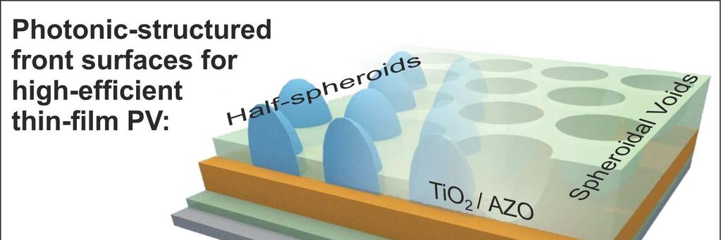
3 Optimal-enhanced Solar Cell Ultra-thinning with Broadband Nanophotonic Light Capture Manuel J. Mendes 1 *, Sirazul Haque, Olalla Sanchez-Sobrado, Andreia Araújo, Hugo Águas, Elvira Fortunato, Rodrigo Martins i3n/cenimat, Department of Materials Science, Faculty of Science and Technology, Universidade NOVA de Lisboa and CEMOP/UNINOVA, Campus de Caparica, Caparica, Portugal *mj.mendes@fct.unl.pt Summary Recent trends in photovoltaics demand ever-thinner solar cells to allow deployment in consumer-oriented products requiring low-cost and mechanically-flexible devices. For that, nanophotonic elements in the waveoptics regime are highly promising, as they capture and trap light in the cells absorber, enabling its thickness reduction while improving efficiency. Here, novel wavelength-sized photonic structures were computationally optimized towards maximum broadband light absorption. Thin-film silicon cells were the test bed to determine the best-performing parameters and study their optical effects. Pronounced photocurrent enhancements, up to 37%, 27% and 48% respectively in ultra-thin (100 and 300nm thick) amorphous and thin (1.5µm) crystalline silicon cells, are demonstrated with honeycomb arrays of semi-spheroidal dome or void-like elements patterned on the cells front. Also importantly, key advantages in the electrical performance are anticipated, since the photonic nano/micro-nanostructures do not increase the cell roughness, therefore not contributing to recombination which is a crucial drawback in state-of-the-art light-trapping approaches. Keywords: Photovoltaics; Nanophotonics; Wave-Optics; Thin-film Solar Cells; Nanostructured Transparent Electrodes 1 Lead Contact 1
4 1. Introduction The application of light trapping (LT) solutions in photovoltaic (PV) devices is considered the most promising route to reduce their thickness while improving sunlight-to-electricity conversion efficiency. LT has been mainly applied to both reduce reflection and boost light absorption in solar cells, allowing thickness reduction while enhancing the generated photocurrent (Polman and Atwater, 2012). Optically-thicker but physically-thinner cells imply cheaper and faster fabrication, light-weight and improved flexibility (Lin et al., 2014; T. Vicente et al., 2018). Besides, thickness reduction can lead to higher open-circuit voltages (and consequently efficiencies) due to lower bulk recombination (Polman et al., 2016). The LT approaches conventionally applied in wafer-based devices rely on textured rear/front surfaces which provide anti-reflection, via geometrical refractive-index matching provided by the front facets, together with light scattering which increases absorption via optical path-length amplification within the absorber layer (Priolo et al., 2014; Andreani et al., 2015). Optimized texturing has shown absorption enhancements in crystalline silicon (c-si) wafers close to the fundamental 4n 2 LT limit of geometrical optics (Ingenito, Isabella and Zeman, 2014). However, when applied in thin-film cells, the textures size must be reduced along with the absorber thickness, which lowers their LT effects (Haug and Ballif, 2015; Branham et al., 2016). Nonetheless, the main drawback of texturing is the fact that it increases roughness (hence surface area) and defect density in the PV material, which deteriorate the cells electrical transport via the increase of charge carrier trapping and recombination. Several alternative strategies have been investigated for thin-film PV, employing nano/micro-structures with dimensions comparable or smaller than the illuminating wavelengths such as: diffraction gratings (Mellor et al., 2011; Schuster et al., 2015), micro-lenses (Mendes et al., 2010; Grandidier et al., 2012; Yang et al., 2016), Mie features (Spinelli, Verschuuren and Polman, 2012; Spinelli and Polman, 2014; Zhou et al., 2014; Van Lare et al., 2015) and plasmonic nanoparticles (Mendes et al., 2014, 2015; Morawiec et al., 2014). However, many of these alternative approaches also require structuring the PV layers, thus suffering from the same electrical compromise of texturing; and none has yet led to efficiencies superior to those attained with optimized periodic texturing, as applied in record-efficient (13.6%) thin-film Si cells (Sai et al., 2015). Presently, the use of high refractive-index dielectric front structures with wavelength-scale features is considered the preferential approach to attain maximum LT in thin-film PV without deteriorating the cells electrical performance (Tseng et al., 2012; Li et al., 2013; Brongersma, Cui and Fan, 2014; Yang et al., 2016; Sanchez-Sobrado et al., 2017). Such nanostructures operate in the complex regime of wave-optics, where interference-related optical mechanisms contribute to LT. Therefore, it is essential to perform optimizations of the full set of physical parameters, employing exact electromagnetic formalisms as in this work, to determine the best-performing materials and geometries. For instance, optimized hexagonal arrays of TiO 2 half-spheroids, integrated in the cell front, can allow 43.3% current enhancement relative to optimized antireflection coatings (ARC) (Mendes et al., 2016). The key advantages of this type of front-located dielectric nanophotonic elements, relative to other LT approaches, are the following. Optically, their combined light incoupling and confinement effects can provide broadband photocurrent enhancement in different portions of the spectrum. This is due to their dome/cone-like shape providing effective index matching with the high- 2
5 index absorber layer, which can almost eliminate reflection at short wavelengths (in UV-Vis) above the PV material bandgap. At the same time, their strong forward-scattering leads to absorption enhancement at the longer near-infrared (NIR) wavelengths close to the bandgap, via light focusing in the intense near-field generated beneath the particles and path-length amplification of the propagating far-field (Mendes et al., 2011). Such optical properties can be tuned by adjusting the particles geometry; thus allowing their customization for different types of PV devices. For instance, shapes with higher aspect ratio exhibit stronger anti-reflection, while lower aspect ratio enables more effective light scattering and coupling to waveguided modes. Electrically, they can be incorporated in the top (front surface) transparent conductive oxide (TCO) of completed cells with flat layers. Thus, the structures do not increase the roughness neither the surface area of the cell layers; and therefore do not degrade the cells electric performance via increase of carrier recombination. The front location of the photonic elements is allowed by their optically lossless dielectric material, in the relevant spectral range, which provides little parasitic absorption. Mechanically, the arrays of photonic elements are not expected to have detrimental effects on the bendability of thin-film cells, relative to flat ARC layers (Yu et al., 2013), enabling their integration on flexible platforms. In this work, such LT strategy is advanced in three ways. First, the design of the photonic structures is developed, considering front-located elements with inverse geometries composed of semi-spheroidal void arrays in the photonic media, which can provide higher degrees of light spreading within the cell absorber layer, and can be more easily fabricated by high-throughput soft-lithography methods. Second, besides highindex dielectric materials, the void nanostructures are developed with TCO (i.e. AZO) media than can improve the cells front contact while providing LT. The enhancements obtained with the TiO 2 dielectric structures are higher than those made of AZO, due to the higher real part and lower imaginary part (associated to parasitic absorption) of TiO 2. Nevertheless, the AZO photonic coatings offer a key electrical advantage since they enable the use of higher TCO volumes in the cells front contact, which decreases its sheet resistance while improving its optical properties. Thirdly, the photonic nanostructures were designed to achieve maximum broadband absorption in different Si layers. Namely, in amorphous silicon (a-si) with 100 nm and 300 nm thickness, and in 1500 nm thick crystalline silicon (c-si); attaining pronounced photocurrent gains (up to 37%, 27% and 48%, respectively). This is highly relevant to minimize the cells thickness with minimal efficiency loss, thereby improving the cells mechanical bendability and facilitating their conformal integration in various flexible substrates [e.g. polymers/plastics (Yu et al., 2013; Nam et al., 2016), fabrics (Qiu et al., 2014), paper-based (Águas et al., 2015; Vicente et al., 2017)] of consumer items such as wearables, smart-packaging/labeling, curved surfaces in buildings or vehicles, internet-of-things systems, mobile medical testing, among others. In addition, flexible cells offer important cost-savings to PV industry, as they can be manufactured in large-area roll-to-roll processes, have reduced material costs due to their small thickness and lower installation costs. A multi-parameter optimization algorithm, implemented in an electromagnetic finite-difference time-domain (FDTD) program, is used to determine the parameters of such structures that provide the highest photocurrent enhancement in thin-film Si cells. The results are compared with the theoretical LT limits of geometrical optics, achieved with idealized Lambertian scattering surfaces (Bozzola, Liscidini and Andreani, 2012; 3
6 Andreani et al., 2015). Such limits neglect light interference effects, therefore are not applicable to the present cell structures with wavelength-sized features and absorber thicknesses. However, they are useful to compare, in order to gain a deeper understanding of the underlying interference-related mechanisms that contribute to LT in our structures in the wave-optics regime (Callahan et al., 2012). The optimizations were conducted for illumination normal to the cells. Therefore, another important aspect analyzed here is how the broadband LT effects are affected for different incidence angles. It was found that, even though the resulting photonic-enhanced current tends to decrease with increasing angle, it remains significantly above that provided by the reference ARC layer for all angles. Thin-film Si cells were the test bed for the light management solutions presented here, but they can be readily implemented in any other type of PV devices. The applicability of our LT schemes is facilitated by the fact that they are not embedded in the cell layer structure, and can be incorporated as a final processing step on top of already-completed cells with a substrate-type layer configuration (termed n-i-p in Si-based devices). Advantageously, such configuration is compatible with nearly all types of thin-film cells, particularly those requiring high-temperature processing as CIGS (Van Lare et al., 2015; Yin et al., 2016); and with the aforementioned flexible applications which typically use opaque bendable substrates (Haug and Ballif, 2015). 2. Results A numerical mesh-based FDTD formalism (Lumerical Solutions, Inc., 2017) was used to model the 3D electricfield distribution produced in the two types of structures shown in Fig. 1. This is a widely employed method to calculate the optical response of thin-film solar cells with photonic structures, having arbitrary materials and geometries (Grandidier et al., 2011; Brongersma, Cui and Fan, 2014; Branham et al., 2016; Mendes et al., 2016; Sanchez-Sobrado et al., 2017). The details of the computational method are given in section S1 of Supplemental Information. A key technological advantage offered by LT is the possibility of lowering the solar cells costs, since it allows reducing the absorber thickness without efficiency loss. Nevertheless, this only makes sense if the LT structures can be fabricated by large-scale inexpensive processes, compatible with PV industry, that do not imply a significant increase in the devices manufacturing price (Polman et al., 2016). For that, scalable softlithography techniques, as nano-imprint (Yin et al., 2016) or colloidal lithography (CL) (Li et al., 2013; Gao et al., 2014; Zhou et al., 2014; Karg et al., 2015), are nowadays considered the preferential nano/microfabrication approaches. In particular, CL allows the engineering of any structure with nano/micrometer resolution and remarkable uniformity throughout indefinitely large areas. This technique uses long-range ordered monolayers of colloidal particles as mask for further pattern transfer. Such colloids are selfassembled in honeycomb arrays whose inter-particle distance can be tuned by dry-etching processes, so the final patterns maintain such periodicity. Therefore, CL naturally forms structures with an hexagonal arrangement, which allows the highest surface packing density, for a given array pitch, among other 2D lattices. This motivated the choice of the arrays of photonic elements considered here, shown in Fig. 1, particularly the void structure of Fig. 1b as described in sub-section
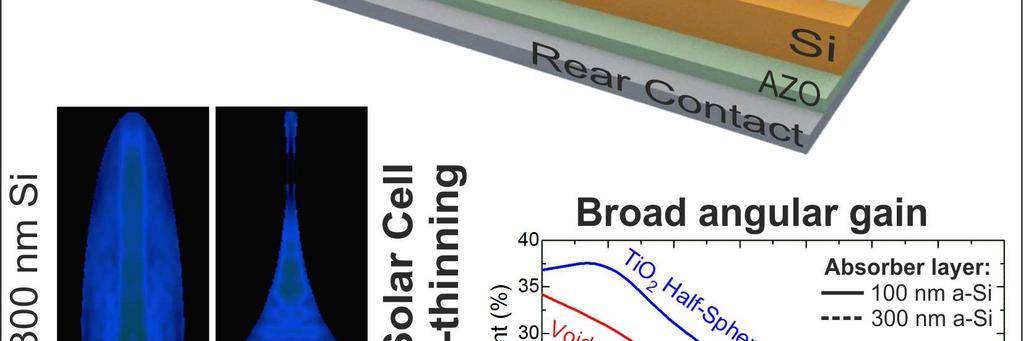
7 In the solar cells, the only absorption (Abs) that generates current is that occurring in the Si layer, while that occurring in the other layers is parasitic as it corresponds to optical losses. Therefore, the figure-of-merit in this work is the photocurrent density (J PH ) which quantifies the full-spectrum absorption occurring in Si by integrating it, convoluted with the AM1.5 solar power spectrum (I AM1.5, units of Wm -2 m -1 ), over the computed wavelength range ( nm) (Branham et al., 2016): = λ h λ. λ dλ (1) where e is the electronic charge, h the Planck constant and c the free-space light speed. This quantity is equivalent to the short-circuit current density that would be produced when electrical losses are neglected; i.e. with an internal quantum efficiency equal to one (IQE=1). An optimization algorithm (described in section S1.3 of Supplemental Information) was used in the FDTD programs to perform a complete screening of the parameters of the LT structures (sketched in Fig. 1) that yield the highest J PH, for three different Si absorber layers in the cells: 100 and 300 nm thick amorphous silicon (a-si) and 1.5 µm thick crystalline silicon (c-si). The results of the optimizations are given in Table 1. Silicon remains the material of choice for PV due to its favorable electro-optical properties, excellent reliability/durability and high abundance (Polman et al., 2016; Vicente, Wojcik, et al., 2017). Thin-film Si cells are attractive due to their potential to be bendable and lightweight. As the rigidity of a layer scales with the third power of its thickness, the ultra-thin (100 nm) a-si absorber considered here is envisaged for highly flexible devices. Such 100 nm layer can be 27 times more flexible than a layer with the conventional thickness (~300 nm) used in standard single-junction a-si cells (Grandidier et al., 2013; Morawiec et al., 2014; Mendes et al., 2015; Vicente, Wojcik, et al., 2017), which is also considered here. Another advantage of scaling down the active layer thickness, particularly in amorphous materials, is that the carrier transport loss can be significantly decreased. However, as light absorption is proportional to the film thickness, the thinner the absorber the more challenging it becomes for LT strategies to maintain a high photocurrent. The 1.5 µm thick c-si absorber is motivated by the recently-demonstrated production of thin (1 20 µm) monocrystalline Si films (Yu et al., 2013; Trompoukis et al., 2015), which can combine the advantages of high material quality (e.g. high open-circuit voltage and fill-factor) and thin-film technologies (e.g. low material cost, flexibility) (Bozzola, Liscidini and Andreani, 2012; Andreani et al., 2015). The present study focuses on the optical response of the materials and does not take into account their electrical quality. That is the reason why the J PH values in Table 1 attained with the 300 nm a-si absorber are generally higher than those with the 1.5 µm c-si, since in the considered spectral range the extinction coefficient (k) of a-si is higher than c-si (see Fig. S1a in Supplemental Information). Nevertheless, here the LT performances are chiefly evaluated by the enhancement in broadband absorption, and consequent J PH, attained with each type of absorber relative to the reference cases without LT structures. The results are compared with two reference cases of unpatterned cells (row 1 in Table 1, layer structure: Mirror/AZO/Si) and cells patterned with a front TCO contact made of AZO, which acts as an anti-reflection coating (ARC, row 2), having a thickness optimized for maximum J PH with each absorber layer (Mendes et al., 2016). AZO was selected as TCO material since optically it performs better as ARC than standard ITO, 5
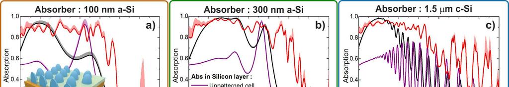
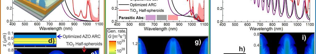
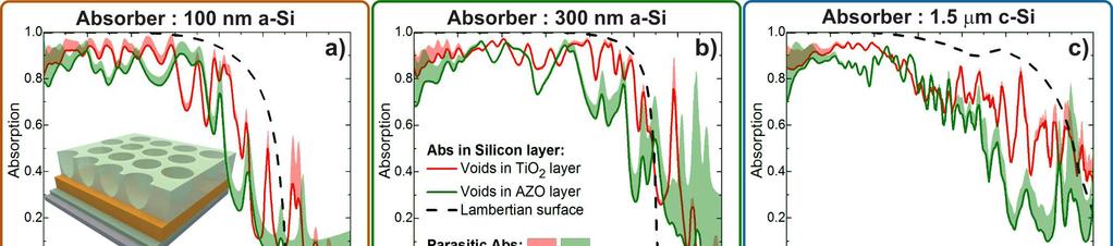
8 with the additional advantage of being composed solely of Earth-abundant materials (Lyubchyk, Vicente, et al., 2016; Lyubchyk, António Vicente, et al., 2016; Yin et al., 2016). The Lambertian light scattering case is also presented (last row in Table 1), computed with an analytical geometrical optics formalism (Bozzola, Liscidini and Andreani, 2012; Branham et al., 2016; Mendes et al., 2016), which consists in an ideal antireflective front surface that randomizes the direction of propagation of incoming light when it enters the cell. This corresponds to the ray-optics LT limit neglecting light interference effects, only valid when the cell thickness is much larger than the illuminating wavelengths. Therefore, this treatment is not accurate with the present thin-film structures but is a standard comparative limit, relevant to analyze not only as benchmark but also to study the physical differences arising from interference-related effects in the wave-optics regime. 2.1 TiO2 half-spheroids array We start by analyzing the hexagonal array of TiO 2 half-spheroids represented in Fig. 1a. The dielectric material and geometrical parameters of this LT structure have been optimized in a previous contribution (Mendes et al., 2016) for the 300 nm a-si and 1.5 µm c-si absorbers. TiO 2 has been identified as one of the preferential materials, for front dielectric LT structures on thin-film cells, due to its high real part of the refractive-index (n), which favors anti-reflection and scattering effects, and low imaginary part (k) which implies reduced parasitic absorption, in the relevant wavelength range (Li et al., 2013; Karg et al., 2015). Here, this study is extended to investigate the optimal LT parameters for the ultra-thin 100 nm a-si absorber, in view of its potential for flexible cells. The results are presented in Fig. 2 and compared with the reference cases of rows 1 and 2 of Table 1. In the planar reference cells (unpatterned and ARC-patterned) the established electric field distributions (thus also the generation rate, G, profiles) are translational invariant, exhibiting planar regions of constructive and destructive interference resulting from the light confinement between the top surface and back reflector (Yin et al., 2016). The consequent 1D Fabry-Perot resonances depend mainly on the Si film thickness and are responsible for the long wavelength absorption peaks observed around 730 and 770 nm wavelengths, respectively with the 100 and 300 nm a-si absorbers, and the peaks for λ 550 nm with 1.5 µm c-si. The optimized ARC layer improves considerably the absorption in the UV-Vis range, relative to unpatterned cells, but not in the NIR. Therefore, it is in the NIR range (λ>700 nm) where the LT elements become more relevant. The main reason is the pronounced scattering effects of the TiO 2 half-spheroids, due to their optimized shape and high real part of the refractive index (n~ ), which trap the light in the high-index Si layers in two ways (Brongersma, Cui and Fan, 2014; Mendes et al., 2016; Yang et al., 2016): 1) the spheroids act as micro-lenses producing a strong forward-scattered near-field that concentrates light in a focal region close to their bottom face, which is particularly important to confine light in the thinner a-si absorbers, as confirmed by the intense G values obtained in Figs. 2e,g ; 2) for long wavelengths with path length above twice the Si layer thickness, the far-field light scattered by the spheroids is redirected to more horizontal directions along the layer, thus traversing a longer path inside Si which can be substantially amplified when coupled with waveguide resonance modes of the structure (Spinelli and Polman, 2014; Van Lare et al., 2015). The low absorption coefficient of Si in this NIR range allows the scattered light to travel a 6
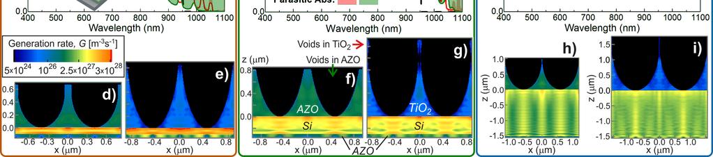
9 long distance along the Si layer, suffering multiple reflections at the top and bottom surfaces and interfering with the scattered waves coming from other particles. Consequently, the hexagonal periodicity of the LT structures imposes guided modes propagating along the absorber plane that give rise to the spectrally sharp resonances observed in the NIR absorption peaks of Fig. 2a-c. These can be viewed as 3D Fabry-Perot resonances, in contrast with the 1D ones in the flat reference cells, as the scattered light waves inside Si interfere both in the in-plane and normal directions, which is evidenced by the dark and bright fringes of the G profiles of Fig. 2. At the UV-Vis wavelengths (λ<700 nm) that do not reach the rear mirror, the absorption enhancement relative to the reference cases is mainly due to the anti-reflection action of the half-spheroids, as their shape provides geometrical effective index matching for the light traveling from air to the higher index Si layer. Similarly to the scattering effects, the optical channeling caused by index matching is favored by a high real part of the spheroids index, as close as possible to that of Si (n~4). In this wavelength range, most light is absorbed up to a depth of ~100 nm in the Si layer, therefore the absorption spectrum attained with the LTenhanced 100 nm a-si cell is similar to those with the thicker layers, for λ<700 nm. This indicates that such LT-enhanced 100 nm cell would constitute an appropriate top sub-cell for a double-junction device. In the half-spheroids structures, the main optical role of the front AZO layer is to act as ARC in the areas between the spheroids. Therefore, the programs converged to values of its thickness (t, see Fig. 1a) similar to those of the optimized ARC cases of row 2 of Table 1. The only exception occurred with the 100 nm a-si absorber, since the corresponding optimized array has a pitch (d=2.2r) close to the spheroids base diameter, thus establishing a close proximity between the particles and, therefore, a stronger overlap of their near-fields. Consequently, the anti-reflection action in this case is solely performed by the TiO 2 half-spheroids, and the presence of an AZO layer in their narrow inter-spaces would simply reduce their optical performance. As a result, the optimization converged to a design without front AZO (t=0). In practical devices, this would require the additional patterning of a top metallic network to realize the front electrical contact (Gao et al., 2014; Knight et al., 2016). Nevertheless, it was observed that there is a significant tolerance of the results with respect to t, as the J PH values for the three different absorbers only change by ~2% when varying t between 0 and 65 nm. Therefore, in the 100 nm a-si solar cell patterned with the optimal half-spheroids array, the application of a t = 65 nm AZO layer as the front contact would still allow high J PH =26.9 ma/cm Spheroidal voids in TiO2 This section analyzes a novel class of front LT nanostructures, represented in Fig. 1b, based on spheroidal void-like geometries which can be viewed as the inverse design of Fig. 1a. As shown in Fig. 3, optimized semi-prolate voids in micrometer (1-2 µm) thick TiO 2 layers yield comparable LT performance as the halfprolate TiO 2 structures of Fig. 2. The J PH values attained with the previous half-spheroids (row 3 of Table 1) are slightly higher (1.8%) than those with the void structures (row 4) for the 100 nm a-si absorber, but lower for the 300 nm a-si (2.5%) and 1.5 µm c-si absorbers (2.8%). Also advantageously for practical implementation, the void arrays can be directly formed by colloidal lithography (CL) methods consisting in four steps (Li et al., 2013; Gao et al., 2014; Karg et al., 2015; Sanchez-Sobrado et al., 2017): 1) wet-coating 7
10 of a close-packed monolayer of colloidal microspheres; 2) shaping the colloids with dry-etching, to form non-close-packed arrays with controllable pitch and aspect ratio of their elements; 3) deposition of the optical material (in this case TiO 2, or AZO in next sub-section); and 4) chemical lift-off of the colloids, leaving the nanostructured material deposited in their inter-spaces and removing that deposited above the particles. This is a versatile soft-lithography method as it can pattern any material that can be deposited in the regions between the shaped colloids. Besides, it is promising for the present LT structures patterned over alreadycompleted cells, since it does not require high-temperature steps (maximum temperature ~100 ºC) or other processes that can degrade the underneath cell layers. It is noteworthy that, despite the considerable differences in the LT designs of Fig. 1a and 1b, the absorption spectra (red curves in Fig. 3a-c) and generation rate profiles (Fig. 3e,g,i) of the cells with the void arrays in a TiO 2 layer present many similarities with those of the half-spheroids of Fig. 2. The overall trends of the useful (occurring in Si) and parasitic absorption curves are the same, but a slight improvement of the Si absorption is observed in the NIR region with the void arrays on the 300 nm a-si and 1.5 µm c-si absorbers. The G profiles are also similar, but those attained with the half-spheroid arrays present more intense and localized hot spots, located close to the Si top surface beneath the particles, due to the stronger lens effect of their round shape which creates highly intense but more confined forward-scattered near-field distributions (Mendes et al., 2011, 2016; Yang et al., 2016). The cross-sectional pyramidal-like geometry, established by the void arrays in the TiO 2 layer, provides less intense hot spots, but allows a more uniform spatial distribution of the absorbed light intensity throughout the entire Si layers. This is attributed to the NIR forward-scattering capabilities of this structure resulting in more extended/spread near-field focal regions along the absorber depth, and higher optical path lengths due to improved far-field LT within the Si. A more delocalized scattered field distribution is beneficial for the thicker 300 nm a-si and 1.5 µm c-si absorbers, as it allows a better performance of these structures particularly in the NIR (see Fig. 3b,c); thus explaining their slightly superior J PH values (row 4 of Table 1) relative to the half-spheroid arrays (row 3). However, the thinner the absorber layer the more advantageous the lens-effect becomes; therefore, with the 100 nm a-si absorber having a lower NIR response, stronger near-field focusing properties are beneficial to effectively concentrate as much light as possible in such ultra-thin active volume. This justifies the higher J PH achieved in this case with the dome-like geometry of the half-spheroids array, relative to that with the voids. The anti-reflection provided by both optimized designs of Fig. 1a and 1b presents little differences, as the absorption in UV-Vis range is ~0.9 for both types of TiO 2 structures. This indicates that the particular dome or pyramidal-like shape of the photonic elements is not crucial to reduce reflection via index matching, and what mainly causes broadband reflection quenching is the high aspect ratio of the high-index structures (Branham et al., 2016). The parasitic losses are represented in Figs. 2a-c and 3a-c by the colored areas between the total absorption of the overall structures (curves not shown) and the absorption only in Si (solid lines). Fig. 2 shows that the parasitic absorption in the AZO layers of the unpatterned and ARC-patterned reference cells is practically negligible, especially with the thicker absorbers. In the cells with the TiO 2 LT structures, the parasitic absorption is more significative but still small relative to the absorption in Si. At UV-Vis wavelengths 8
11 (λ<700 nm), such optical losses occur mainly in the front TiO 2 material; but at longer wavelengths TiO 2 is practically non-absorbing, so the losses chiefly take place in AZO due to the free carrier absorption of TCO materials in the NIR. Most of this absorption takes place at the rear 60 nm AZO passivating layer, present in all structures, and is boosted by the light scattering effects of the photonic elements and their coupling with the rear mirror (Mendes et al., 2016). This is demonstrated by the bright colors of the G distributions in the rear AZO layers of Figs. 2 and 3e,g,i, relative to those of the ARC cases of Fig. 2d,f,h. The absorption spectra in Fig. 3a-c are compared to the corresponding Lambertian LT case for each Si absorber, determined analytically in the geometrical optics regime (Bozzola, Liscidini and Andreani, 2012; Andreani et al., 2015; Branham et al., 2016). Such so-called Lambertian limit is not applicable to our structures with thicknesses and photonic features below or close to the incident wavelengths, but it is nonetheless important to analyze as previously mentioned. Figs. 2a-c and 3a-c show that the optimized TiO 2 LT structures enable Si absorption values close but slightly below the Lambertian curves throughout most of the spectrum, with the biggest discrepancy observed for the cases with the 1.5 µm c-si absorber where geometrical optics predicts a quite high maximum photocurrent (38 ma/cm 2 row 6 in Table 1), almost reaching that of bulk wafer-based cells. As wavelength increases, the extinction coefficient (k) of the Si materials (see Fig. S1a) becomes lower and approaches zero at the longer NIR wavelengths of belowbandgap photons, which explains the abrupt decrease of the Lambertian absorption curves for λ 900 nm and 1 µm, respectively for the a-si and c-si absorbers. However, the omnidirectional scattering ability of the wave-optical elements and, essentially, the coupling of their scattered light with waveguided modes trapped in the Si layer, allow extending the cells NIR response to wavelengths longer than those allowed by geometrical optics; particularly at the sharp Fabry-Perot resonances of the thinner a-si structures which generate the sharp absorption peaks for λ>950 nm (Yu et al., 2013; Mendes et al., 2016; Yang et al., 2016). 2.3 Spheroidal Voids in AZO Despite the advantageous optical properties of TiO 2 for photonic nanostructures located on the cells front, its poor conductivity makes it difficult to engineer a good-performing front contact for the devices. With the LT structures of Fig. 1b analyzed in sub-section 2.2, such contact could be realized by patterning a top metallic network, or micro-meshed electrodes, deposited on Si prior to the TiO 2 (Gao et al., 2014; Knight et al., 2016). This is a promising approach mainly for thin c-si active layers, as the 1.5 µm thick one studied here. However, for a-si cells, metallic grids alone may not be sufficient for efficient charge extraction due to the low carrier diffusion lengths in such amorphous materials (~0.1-1 µm as compared to mm in c-si). Therefore, a good-performing front TCO layer is especially crucial for a-si devices. As such, we now consider the same LT design of the previous sub-section (Fig. 1b) but using AZO as the material of the photonic layer, instead of TiO 2. The abundance, non-toxicity and excellent transparency and electrical properties of AZO make this material being currently regarded as the best alternative to the standard ITO transparent contacts, whose price is growing exponentially due to scarcity of indium (Lyubchyk, Vicente, et al., 2016; Lyubchyk, António 9
12 Vicente, et al., 2016; Marouf et al., 2017). Several approaches have been investigated to integrate LT structures in ZnO-based films (Battaglia et al., 2011; Despeisse et al., 2011), including growth of pyramids by chemical deposition, wet-etching of crater-like structures, nano-texturing by imprint/moulding, among others. However, so far these approaches have been applied on the TCO front contact of thin-film Si cells with a superstrate configuration, where the Si layer is conformally deposited over the textured ZnO-based material. Although this can be optically effective, the additional roughness induced in the PV layers by the texturing degrades the devices electrical performance, as previously described, hindering the benefits of such LT schemes. Therefore, here an innovative design is optimized where the wavelength-scale structured AZO is patterned on top of the flat cell layers (see Fig. 1b); so the present approach is not affected by the traditional compromise between optical gains and electrical losses, as the photonic elements do not increase the devices roughness. The results of the optimized void-structured AZO layers are presented in Fig. 3, together with those of the TiO 2 structures with the design of Fig. 1b, and the corresponding J PH values are listed in row 5 of Table 1. Even though substantial photocurrent enhancements are determined with such AZO front structures, relative to the optimized ARC cases (row 2 of Table 1), they are considerably lower than those attained with TiO 2 (row 4). This is verified by the lower Si absorption values of the solid green curves in Fig. 3a-c, relative to the red curves, throughout the analyzed spectra; in accordance with the lower values of generation rate shown in the G profiles of Fig. 3d,f,h along most of the Si volume. The AZO LT structures perform optically worse than the TiO 2 ones, in terms of anti-reflection and scattering, due to the worse components of its complex refractive-index (plotted in Fig. S1b of Supplemental Information): 1) Real part of refractive index (n) For anti-reflection via geometrical index matching, n should be ideally close to that of Si (n~4) to favor the light incoupling from air towards such high-index absorber. Therefore, high-index dielectric materials as TiO 2 (n~ ) provide a better impedance matching of sunlight than lower index materials like AZO (n~ ). Regarding the scattering performance affecting mainly the NIR, the higher the n the higher can be the scattering cross-sections of the photonic features which lead to more intense near and far-fields inside the cell absorber. Nevertheless, note that increasing n alone may not always guarantee photocurrent enhancement, since it amplifies the degree of interference caused by the photonic structure which influences, for instance, the magnitude, spatial extension and location of the light focusing beneath its features. So, it is crucial to appropriately adjust the geometrical parameters of the structures for each n, as also investigated in previous contributions (Mendes et al., 2010, 2011, 2016), to optimally tune: 1) the near-field focal region to cover the depth of the underneath absorber layer, which mainly depends on the shape of the photonic elements; and 2) the far-field propagating light, in particular the waveguide mode coupling which is chiefly influenced by the arrays periodicity (pitch). This reveals the importance of using multi-parameter optimizations, as performed here, which take into account such dependencies by searching for the best combination of parameters that maximize the J PH. 2) Imaginary part of refractive index (k) As seen in Fig. S1b, the k of AZO is superior to that of TiO 2, particularly in the NIR where it becomes three orders of magnitude higher. Therefore, the AZO LT structure provides much higher parasitic losses for λ 700 nm. This is shown in Fig. 3a-c and also in the G 10
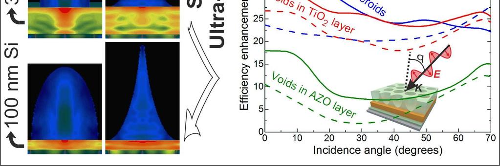
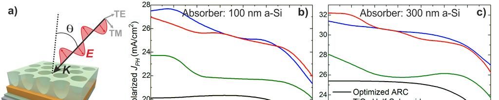
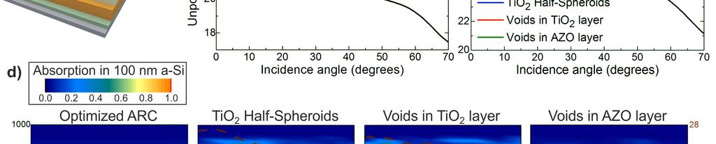
13 profiles (Fig. 3d-i) that present much higher values inside the front AZO structures. The relatively high k of this material led the optimizations to converge to smaller AZO features, with thickness values t considerably lower than those of the TiO 2 structures (see rows 4 and 5 of Table 1). In the present LT geometry, the width of the nanophotonic elements (i.e. base length of the pyramidal features viewed in the cross section profiles of Fig. 3d-i) is equal to the array pitch, d, as sketched in Fig. 1b. In general, the thicker the absorber the more its absorption onset can be extended to longer NIR wavelengths; so such optimal width tends to increase with Si thickness to strengthen the scattering effects along the full NIR photo-response of the cells. However, increasing the features width alone would imply decreasing their aspect ratio, which would reduce their anti-reflection effects. Therefore, the optimal layer thickness t, determining the features height, must simultaneously increase to ensure the smoothest possible variation of the effective index seen by the incoming light. This explains the monotonous increase of the values of d and t (rows 4 and 5 of Table 1) with the absorber thickness, as also seen in the profiles of Fig. 3d-i. 2.4 Angular study The LT structures in the previous sub-sections were optimized for illumination incident normal to the cells. Nevertheless, for practical PV applications it is important to analyze the cells response to different incidence angles, particularly with thin-film devices that are usually not mounted on sun-tracking platforms. In addition, if the cells are flexible they can operate in a bent state having a range of incidence angles shining throughout their active area. Therefore, if their response is not omnidirectional, a photocurrent reduction in one portion of the area can cause an overall drop in the total current supplied by the cells. In view of the above, it is advantageous to implement LT structures able to provide J PH values as high and independent as possible of the incidence angle (Wilken et al., 2015). This is especially relevant for the thinner 100 nm a-si cells, as they can be much more flexible than those with the other thicker absorbers. Therefore, here we focus in the angle-resolved optical response for the different LT structures on the ultrathin 100 nm a-si layer, shown in Fig. 4. At oblique incidence, such response depends on the polarization of incident light, so it is important to also analyze both TM (transverse magnetic) and TE (transverse electric) components separately (see Fig. 4a,d). As sunlight is unpolarized, the output current is given by the average between the photocurrent values attained with each component. The angle dependence of the unpolarized J PH is shown in Fig. 4b and compared with that in Fig. 4c attained employing the thicker 300 nm a-si absorber layer. The FDTD computations of the angular-dependent optical response, used to determine the results of Fig. 4, have been corroborated by comparison with the analytical transfer-matrix method for planar solar cell structures, as shown in section S2 of the Supplemental Information. Generally, the J PH tends to decrease with increasing incidence angle (θ, see Fig. 4a). At angles up to ~50º, such decrease only occurs in cells with the LT structures, due to the reduction of Si absorption in the NIR as seen in Fig. 4d, since the scattering and waveguide mode coupling provided by the photonic arrays are not optimized for oblique incidence. Still, with both TiO 2 LT structures, moderate absorption peaks appear at certain angles in the NIR, caused by Fabry-Perot resonances excited for such illumination directions; which are less evident with the void arrays in AZO due to the parasitic losses of this material at longer wavelengths. 11
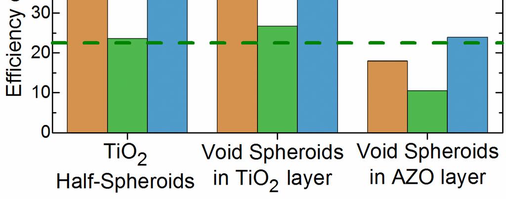
14 The general decrease of photocurrent for angles from 0 to ~50º is not observed with the flat reference ARC structure, since it does not exhibit NIR scattering effects. For angles above ~50º, the unpolarized J PH of both the LT and ARC structures drops abruptly mainly due to the increase in reflection from the front surface (Wilken et al., 2015), explaining the decrease in the UV-Vis absorption observed in Fig. 4d at such higher angles. This originates from common Brewster-type effects, causing a drop in the reflection of the TM component and an increase in the reflection of the TE component. Therefore, the TE light absorption in Si drops more abruptly at such high angles, while the TM absorption can even increase at certain wavelengths (Spinelli, Verschuuren and Polman, 2012), as seen by the peaks in the nm range on the right of the top contour plots of Fig. 4d. Such TM peaks are the main responsibles for the maxima observed in the J PH curves of Fig. 4b,c at angles in the ~50-65º range. 3. Discussion The core design rule of the LT schemes investigated in this work is that they improve the cells light harvesting without roughening their thin PV layer, in contrast with conventional texturing/structuring-based LT approaches. This was pursued by optimizing the combined anti-reflection and scattering properties of distinct front nanophotonic arrays, which do not increase the defect density (recombination) in the PV material as they are implemented over the unstructured planar absorber layer. As such, we were able to fully optimize the LT geometries towards their maximum optical performance, without concerns relative to the devices electrical performance. Therefore, the efficiency gains resulting from the LT structures presented here are expected to be similar to their corresponding J PH enhancements. The bar graph of Fig. 5 shows such predicted gains, relative to the optimized ARC case of row 2 of Table 1, and compares them with those analytically determined in the Lambertian case of geometrical optics (row 6 of Table 1). Note that the Lambertian enhancements were not calculated relative to the same reference values (ARC cases of Table 1) of the optimized LT structures, but rather relative to the same theoretical structure but without light scattering from the front surface (Bozzola, Liscidini and Andreani, 2012; Mendes et al., 2016). For the three types of LT nanostructures explored in this work, the highest photocurrent enhancements are attained with the 1.5 µm c-si absorber and the lowest with the 300 nm a-si. Such trend follows that predicted for the Lambertian cases, shown by the dashed lines of Fig. 5 and analyzed in further detail in previous contributions (Bozzola, Liscidini and Andreani, 2012; Callahan et al., 2012; Mendes et al., 2016). The highest enhancement values achieved with 1.5 µm c-si are due to the fact that c-si is an indirect bandgap semiconductor with a lower extinction coefficient in most of the analyzed spectral range (see Fig. S1a) than a-si, which is a more absorbing direct semiconductor. Therefore, thin c-si cells can benefit more from LT than a-si ones, since c-si requires higher dwelling time (path length) of the photons in the active region, as provided by scattering, to complete the absorption of the full range of above-bandgap photons before they escape the device (Andreani et al., 2015; Trompoukis et al., 2015). On the other hand, generally LT also becomes more beneficial with decreasing cell thickness, since the thinner the Si layer the more pronounced can be the absorption enhancement, as analytically computed with geometrical optics. Consequently, higher enhancements were obtained with the 100 nm a-si absorber relative to the 300 nm a-si. Nevertheless, as seen 12
15 in Fig. 5, the 300 nm a-si absorber reached enhancements above that of the corresponding Lambertian case (22.5%), particularly with the TiO 2 voids. This is because such LT structure produced pronounced absorption peaks at NIR wavelengths (λ>950 nm) above the onset of the Lambertian absorption spectrum (see Fig. 3b), which originate from wave-optical interference effects resulting from the coupling of the scattered light with guided modes trapped by multiple reflections in the cell (Callahan et al., 2012). However, it should be noted that the absolute values of the maximum J PH given in Table 1 are below those of the Lambertian limits (row 6) for all the LT structures optimized here. The TiO 2 void structure introduced in this work allowed the highest enhancements (26.4% and 47.5%, respectively) for the 300 nm a-si and 1.5 µm c-si absorbers, as its cross-sectional pyramidal shape provides effective anti-reflection at short (UV-Vis) wavelengths and a better coverage of the forward-scattered field throughout such Si layers, relative to the TiO 2 half-spheroids. The dome shape of the half-spheroids provides a higher optical lens effect which results in a stronger localization of the forward-scattered light. Such effect is, however, advantageous for light confinement in ultra-thin absorber layers, as demonstrated by the highest current enhancement (37.0%) attained with the 100 nm a-si absorber topped with the half-spheroids array. The lowest enhancements in Fig. 5 were obtained with the AZO void arrays due to the weaker anti-reflection and scattering effects allowed by this material, as a consequence of its lower real part of the refractive-index relative to TiO 2, and its higher parasitic losses mainly in the NIR range (see Fig. S1b). Despite such more modest enhancements (11-24%), this AZO LT structure offers an unprecedented practical advantage: it constitutes the TCO front electrode of the cell, allowing the use of higher TCO volume (hence yielding lower contact resistance) relative to that employed conventionally. The volume of front AZO (V AZO ) in the LT structure of Fig. 1b is determined by subtracting the volume of the semi-prolate holes from the total parallelepiped layer volume. Dividing the resulting AZO volume by its covered area (A AZO ) yields a volumeequivalent layer thickness (t eq =V AZO /A AZO ) equal to 319, 490 and 387 nm, respectively for the AZO LT structures on the 100 nm, 300 nm a-si and 1.5 µm c-si cells. Such t eq values are considerably higher than the layer thicknesses used in conventional flat TCO front contacts which typically range from nm (as in the reference ARC cases considered here) to nm in n-i-p thin-film Si cells (Grandidier et al., 2012; Morawiec et al., 2014; Águas et al., 2015; Mendes et al., 2015), depending on the TCO material. Higher layer thicknesses lead to detrimental optical losses with flat TCOs, but not with photonic-structured TCOs as those optimized here. Therefore, the AZO void structure can provide, in practice, higher efficiency enhancements than those predicted in Fig. 5, as it may increase not only the generated current but also the cells fill-factor due to the reduction of series resistance of the front contact. 3.1 Comparison with other light trapping (LT) approaches As the main role of LT is the improvement of light absorption in the PV layer, the LT performance is commonly evaluated by the photocurrent enhancement achieved relative to planar reference solar cells without the LT structures but with an optimized single-layer ARC, as performed in this work. In commercial wafer-based c-si cells the texturing is applied on the front surface of the absorber, so this approach is difficult to implement in thin film cells since the dimensions of the texturing features ( 1 µm) 13
16 (Ingenito, Isabella and Zeman, 2014) are usually higher or comparable to the cells thickness. Nevertheless, when applying optimized texturing on the front of thin (5 µm) c-si wafers a maximum enhancement of 37% has been attained (Branham et al., 2016). In thin film Si cells with a n-i-p layer configuration, compatible with opaque substrates, LT is commonly based on texturing the cells substrate. This is performed, for instance, by employing the Asahi standard textured substrate widely used in industrial devices, which has been shown to provide about 20% and 37% photocurrent enhancement in conventional 350 nm a-si (Van Lare et al., 2015) and 1.5 µm µc-si (Mendes et al., 2015) cells, respectively. When the morphology of the substrate corrugations is controlled with lithographic processes, for example employing a 2D photonic grating of dielectric nanocavities, higher enhancements can be reached (23% in 350 nm a-si) (Van Lare et al., 2015). Alternative wave-optical solutions, based in front-located dielectric elements on planar solar cells, have mainly considered self-assembled monolayers of spherical colloids [e.g. silica (Grandidier et al., 2012) or TiO 2 (Yang et al., 2016) patterned on 100 nm a-si cells]. Despite the fabrication simplicity, the silica particles allowed only modest 10-15% current enhancements due to their low refractive-index; while with the TiO 2 particles a much higher enhancement of 43% is modeled but relative to a non-optimized 80 nm ITO ARC. Superior performances can be attained with higher aspect ratio dome/pyramidal-like geometries, mainly due to the better geometrical index matching that they provide for broadband anti-reflection, which is the class of structures optimized in this work. Sets of this type of TiO 2 LT front structures with close-packed features have been optically modeled (Tseng et al., 2012), yielding a maximum 33% photocurrent enhancement in 2 µm c-si cells. The best J PH enhancements indicated in Fig. 5 for the TiO 2 LT structures (37%, 27% and 48% in 100 nm a-si, 300 nm a-si and 1.5 µm c-si, respectively) are among the highest attained so far in the literature, when comparing the values for similar Si absorbers. Apart from the favorable choice of geometries and material of the LT elements investigated here, our superior results are chiefly attributed to a complete multi-variable optimization process (see section S1.3 in Supplemental Information) that explored the full domains of the main parameters of the photonic structures, in contrast with most related studies limited to certain parameter sets or to sequential parameter sweeps (Tseng et al., 2012). When more than 2 parameters are involved, such sweeps are not effective in finding the global maximum of figures-of-merit of complex systems that have a strong inter-dependence between the parameters, as in the present regime of wave-optics. Therefore, the multi-parameter optimizations performed in this work enabled the design of LT-enhanced cells capable of producing photocurrent density values (up to 27.5, 32.2 and 32.0 ma/cm 2 in 100 nm a-si, 300 nm a-si and 1.5 µm c-si, respectively) approaching those (32.9 ma/cm 2 ) of the present record thin-film (~4 µm thickness) Si single-junction cell, fabricated on an optimized honeycomb-textured substrate but using a much thicker microcrystalline Si layer (Sai et al., 2015). As the LT structures developed here do not compromise the cells electrical performance, they can thereby allow PV devices with improved efficiencies using thinner absorber layers, which enable additional advantages such as lower material costs and mechanical bendability. 14
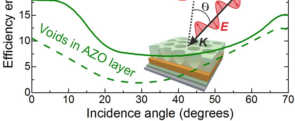
17 3.2 Angular dependence of light collection enhancement Regarding the angular dependence analysis (section 2.4), while the J PH attained with the optimized ARC is approximately maintained from 0 to ~50º, that with the LT structures drops by about 15-20% in this angular range due to the weakening of the scattering effects. Nevertheless, the J PH provided by the LT structures remains above that of the ARC case for the entire 0-70º angular range, as shown by the enhancement curves in Fig. 6. In general, such enhancement tends to decrease with increasing angle up to ~40º; but then increases for higher angles due to the reduction of the anti-reflection effects, which causes a more abrupt photocurrent drop for the ARC case in this higher-angle range than for the LT cases. In the continuation of the values in Fig. 5 for normal incidence, the enhancements attained in the 100 nm a-si cells remain above those with the 300 nm a-si absorber, for practically all angles. However, the separation between the curves of these absorbers becomes smaller with increasing angle, which is expected as light impinges on the structures from a more horizontal (in-plane) direction that is less sensitive to the cell thickness. 4. Conclusions The goal of reaching high-efficient (>20 %), inexpensive (<1$/W) and flexible (bending radius 5 mm) solar cells, amenable to industrial implementation, is currently one of the hottest research topics in PV where light management has shown to be indispensable. The findings presented here are an essential contribution in this context, to realize ever thinner cells with optimized light harvesting and electronic transport. Two classes of front-located LT nanostructures, composed of wavelength-sized features, were computationally designed to maximize absorption in the underlying PV layer without degrading the devices electrical performance. The optical roles of such structures have been demonstrated by: 1) drastically reducing reflection losses at short wavelengths (above the absorber bandgap) via geometrical refractive index matching with the cell media; and 2) enhanced absorption of longer wavelengths by increasing their path length via light bending and coupling with waveguided modes confined in the absorber layer. These combined effects provide broadband absorption enhancement which allows reducing the absorber thickness without lowering its output current. Here, it is important to underline that our results demonstrate that such optical effects perform remarkably well with LT structures having quite distinct designs, as those investigated (see Fig. 1), as long as their parameters are fully optimized. This is quite relevant, especially for industrial implementation, as it yields more versatility in the choice of the photonic structures, enabling the integration of the design that is more convenient for large-scale fabrication. Although the structures have been optimized for absorption enhancement in thin-film Si cells, the insights gained are generic and can be straightforwardly applied to any type of thin-film PV devices, with distinct materials or thickness, by careful tuning the physical parameters analyzed here. Acknowledgments 15
18 This work was funded by FEDER funds, through the COMPETE 2020 Program, and national funds, through the Portuguese Foundation for Science and Technology (FCT-MEC), under the projects POCI FEDER (Reference UID/CTM/50025) and ALTALUZ (Reference PTDC/CTM-ENE/5125/2014). The authors acknowledge partial funding from the European Projects BET-EU (H2020-TWINN-2015, grant ) and 1D-NEON (H2020-NMP-2015, grant ). M. J. Mendes also acknowledges funding by the EU FP7 Marie Curie Action FP7-PEOPLE-2013-IEF through the DIELECTRIC PV project (grant ) and FCT-MEC through the grant SFRH/BPD/115566/2016. O. Sanchez-Sobrado and A. Araújo acknowledge FCT-MEC through grants SFRH/BPD/114833/2016 and SFRH/BD/85587/2012, respectively. Author Contributions M.J.M. conceived the modeling programs, performed the simulations and wrote the manuscript. S.H. performed the angular study simulations and corresponding analysis. O.S.S., A.A. and H.A. assisted in projecting the theoretical investigations presented here, revised the manuscript and discussed the results. E.F. and R.M. revised the manuscript and supervised the work and financing projects. Declaration of Interests The authors declare no competing interests. References Águas, H. et al. (2015) Thin Film Silicon Photovoltaic Cells on Paper for Flexible Indoor Applications, Advanced Functional Materials, 25(23), pp doi: /adfm Andreani, L. C. et al. (2015) Photonic light trapping and electrical transport in thin-film silicon solar cells, Solar Energy Materials and Solar Cells. Elsevier, 135, pp doi: /j.solmat Battaglia, C. et al. (2011) Nanomoulding of transparent zinc oxide electrodes for efficient light trapping in solar cells, Nat. Photon., 5(9), pp doi: /nphoton Bozzola, A., Liscidini, M. and Andreani, L. C. (2012) Photonic light-trapping versus Lambertian limits in thin film silicon solar cells with 1D and 2D periodic patterns, Optics Express. Optical Society of America, 20(S2), p. A224. doi: /OE.20.00A224. Branham, M. S. et al. (2016) Empirical Comparison of Random and Periodic Surface Light-Trapping Structures for Ultrathin Silicon Photovoltaics, Advanced Optical Materials, 4(6), pp doi: /adom Brongersma, M. L., Cui, Y. and Fan, S. (2014) Light management for photovoltaics using high-index nanostructures, Nature Materials. Nature Publishing Group, a division of Macmillan Publishers Limited. All Rights Reserved., 13(5), pp doi: /nmat3921. Callahan, D. M. et al. (2012) Solar Cell Light Trapping beyond the Ray Optic Limit, pp Despeisse, M. et al. (2011) Optimization of thin film silicon solar cells on highly textured substrates, physica status solidi (a). WILEY-VCH Verlag, 208(8), pp doi: /pssa Gao, T. et al. (2014) Uniform and Ordered Copper Nanomeshes by Microsphere Lithography for Transparent Electrodes, Nano Letters. American Chemical Society, 14(4), pp doi: /nl Grandidier, J. et al. (2011) Thin-film solar cells: light absorption enhancement in thin-film solar cells using whispering gallery modes in dielectric nanospheres, Advanced Materials. WILEY-VCH Verlag, 23(10), p Available at: Grandidier, J. et al. (2012) Solar cell efficiency enhancement via light trapping in printable resonant dielectric nanosphere arrays, physica status solidi (a). WILEY-VCH Verlag, 210(2), pp doi: /pssa Grandidier, J. et al. (2013) Solar cell efficiency enhancement via light trapping in printable resonant dielectric nanosphere arrays, physica status solidi (a). WILEY-VCH Verlag, 210(2), pp doi: /pssa Haug, F.-J. and Ballif, C. (2015) Light management in thin film silicon solar cells, Energy Environ. Sci. Royal Society of Chemistry, 8(3), pp doi: /C4EE03346A. Ingenito, A., Isabella, O. and Zeman, M. (2014) Experimental Demonstration of 4n 2 Classical Absorption Limit in Nanotextured Ultrathin Solar Cells with Dielectric Omnidirectional Back Reflector, ACS Photonics, 1(3), pp
19 doi: /ph Karg, M. et al. (2015) Colloidal self-assembly concepts for light management in photovoltaics, Materials Today, 18(4), pp doi: Knight, M. W. et al. (2016) Soft imprinted Ag nanowire hybrid electrodes on silicon heterojunction solar cells, Nano Energy. Elsevier, 30(October), pp doi: /j.nanoen Van Lare, C. et al. (2015) Dielectric Scattering Patterns for Efficient Light Trapping in Thin-Film Solar Cells, Nano Letters, 15(8), pp doi: /nl Li, X. H. et al. (2013) Light trapping in thin-film solar cells via scattering by nanostructured antireflection coatings, Journal of Applied Physics, 114(4). doi: / Lin, Q. et al. (2014) Flexible photovoltaic technologies, Journal of Materials Chemistry C, 2, pp doi: /c3tc32197e. Lumerical Solutions, Inc. (2017) Lumerical Solutions, Inc. Available at: (Accessed: 1 February 2018). Lyubchyk, A., Vicente, A., et al. (2016) Influence of post-deposition annealing on electrical and optical properties of ZnObased TCOs deposited at room temperature, Physica Status Solidi (A) Applications and Materials Science, 213(9), pp doi: /pssa Lyubchyk, A., Vicente, A., et al. (2016) Mapping the Electrical Properties of ZnO-Based Transparent Conductive Oxides Grown at Room Temperature and Improved by Controlled Postdeposition Annealing, Advanced Electronic Materials, 2(1), p doi: /aelm Marouf, S. et al. (2017) Low-temperature spray-coating of high-performing ZnO:Al films for transparent electronics, Journal of Analytical and Applied Pyrolysis, 127, pp doi: /j.jaap Mellor, A. et al. (2011) Upper limits to absorption enhancement in thick solar cells using diffraction gratings, Progress in Photovoltaics: Research and Applications. John Wiley & Sons, Ltd., 19(6), pp doi: /pip Mendes, M. J. et al. (2010) Near-field scattering by dielectric spheroidal particles with sizes on the order of the illuminating wavelength, J. Opt. Soc. Am. B. OSA, 27(6), pp Available at: Mendes, M. J. et al. (2011) Light concentration in the near-field of dielectric spheroidal particles with mesoscopic sizes, Optics Express, 19(17), p doi: /OE Mendes, M. J. et al. (2014) Colloidal plasmonic back reflectors for light trapping in solar cells., Nanoscale, 6(9), pp doi: /c3nr06768h. Mendes, M. J. et al. (2015) Broadband light trapping in thin film solar cells with self-organized plasmonic nano-colloids., Nanotechnology. IOP Publishing, 26(13), p doi: / /26/13/ Mendes, M. J. et al. (2016) Design of optimized wave-optical spheroidal nanostructures for photonic-enhanced solar cells, Nano Energy. Elsevier, 26, pp doi: /j.nanoen Morawiec, S. et al. (2014) Broadband photocurrent enhancement in a-si:h solar cells with plasmonic back reflectors, Optics Express. OSA, 22(S4), pp. A1059 A1070. doi: /oe.22.0a1059. Nam, J. et al. (2016) Transfer Printed Flexible and Stretchable Thin Film Solar Cells Using a Water-Soluble Sacrificial Layer, Advanced Energy Materials, p. n/a-n/a. doi: /aenm Polman, A. et al. (2016) Photovoltaic materials present efficiencies and future challenges, Science, 352, p doi: /science.aad4424. Polman, A. and Atwater, H. A. (2012) Photonic design principles for ultrahigh-efficiency photovoltaics, Nat Mater. Nature Publishing Group, a division of Macmillan Publishers Limited. All Rights Reserved., 11(3), pp Available at: Priolo, F. et al. (2014) Silicon nanostructures for photonics and photovoltaics, Nature Nanotechnology. Nature Publishing Group, 9(1), pp doi: /NNANO Qiu, L. et al. (2014) Integrating perovskite solar cells into a flexible fiber, Angewandte Chemie - International Edition, 53(39), pp doi: /anie Sai, H. et al. (2015) Triple-junction thin-film silicon solar cell fabricated on periodically textured substrate with a stabilized efficiency of 13.6%, Applied Physics Letters, 106(21), p doi: doi: Sanchez-Sobrado, O. et al. (2017) Colloidal-lithographed TiO2 photonic nanostructures for solar cell light trapping, Journal of Materials Chemistry C. The Royal Society of Chemistry, 5(27), pp doi: /C7TC01756A. Schuster, C. S. et al. (2015) Plasmonic and diffractive nanostructures for light trapping - an experimental comparison, Optica. OSA, 2(3), pp doi: /optica Spinelli, P. and Polman, A. (2014) Light Trapping in Thin Crystalline Si Solar Cells Using Surface Mie Scatterers, IEEE J. Photovoltaics, 4(2), pp Spinelli, P., Verschuuren, M. A. and Polman, A. (2012) Broadband omnidirectional antireflection coating based on subwavelength surface Mie resonators, Nat Commun. Nature Publishing Group, a division of Macmillan Publishers Limited. All Rights Reserved., 3, p doi: T. Vicente, A. et al. (2018) Multifunctional cellulose-paper for light harvesting and smart sensing applications, Journal of Materials Chemistry C. The Royal Society of Chemistry, 6(13), pp doi: /C7TC05271E. Trompoukis, C. et al. (2015) Photonic nanostructures for advanced light trapping in thin crystalline silicon solar cells, physica status solidi (a), 212(1), pp doi: /pssa Tseng, P.-C. et al. (2012) Antireflection and light trapping of subwavelength surface structures formed by colloidal 17
20 lithography on thin film solar cells, Progress in Photovoltaics: Research and Applications. John Wiley & Sons, Ltd, 20(2), pp doi: /pip Vicente, A. T., Wojcik, P. J., et al. (2017) A statistics modeling approach for the optimization of thin film photovoltaic devices, Solar Energy, 144, pp doi: /j.solener Vicente, A. T., Araújo, A., et al. (2017) Optoelectronics and Bio Devices on Paper Powered by Solar Cells, in Nanostructured Solar Cells. InTech. doi: / Wilken, K. et al. (2015) Light Management in Flexible Thin-Film Solar Cells The Role of Nanoimprinted Textures and Tilted Surfaces, IEEE Journal of Photovoltaics, 5(6), pp doi: /JPHOTOV Yang, Z. et al. (2016) Scattering effect of the high-index dielectric nanospheres for high performance hydrogenated amorphous silicon thin-film solar cells, Scientific Reports. Nature Publishing Group, 6, p doi: /srep Yin, G. et al. (2016) Optoelectronic Enhancement of Ultrathin CuIn 1-x Ga x Se 2 Solar Cells by Nanophotonic Contacts, Advanced Optical Materials, p doi: /adom Yu, K. J. et al. (2013) Light trapping in ultrathin monocrystalline silicon solar cells, Advanced Energy Materials, 3(11), pp doi: /aenm Zhou, D. et al. (2014) Optimization of the optical properties of nanostructured silicon surfaces for solar cell applications, Journal of Applied Physics, 115(13). doi: /
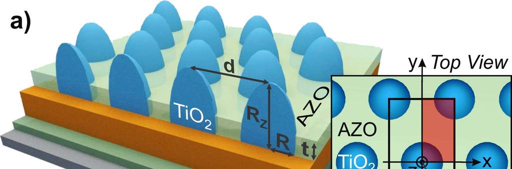
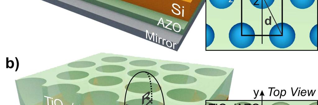
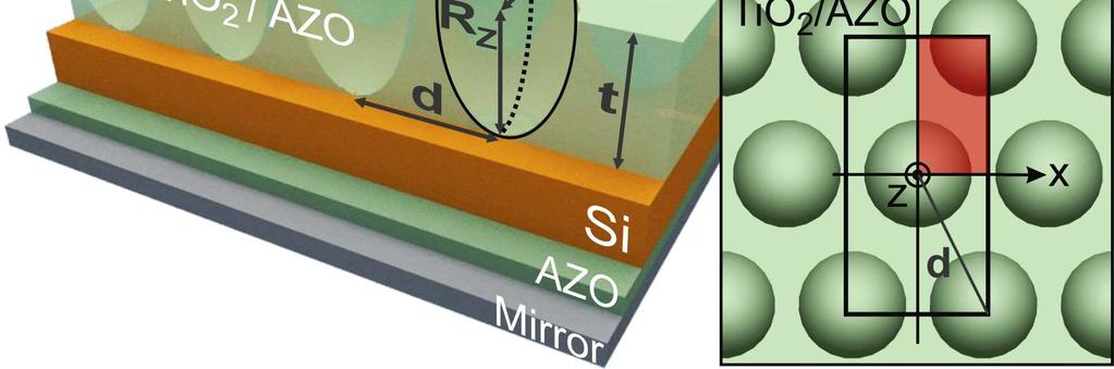
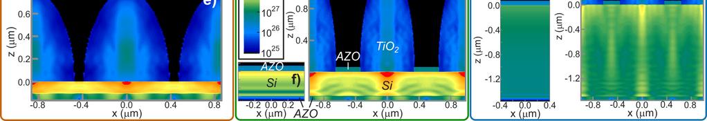
21 Figure titles and legends Figure 1. Sketches of both types of LT nanostructures analyzed in this work, patterned on solar cells with a Si absorber (either a-si or c-si). The LT elements provide a gradually varying effective refractive-index which minimizes reflection, while their geometry can interact with the incoming light to produce strong scattered fields preferentially directed into the higher-index Si material with high mode density. The parameters (R, R Z, t, d) considered for optimization are indicated by the arrows. The LT structures consist in an hexagonal array (with pitch d) of vertically-aligned spheroidal-based features with radii R and R Z, respectively along the in-plane and normal directions: a) TiO 2 half-prolates separated by an AZO layer with thickness t; b) semi-prolate voids in a layer of either TiO 2 or AZO material with thickness t. At normal incidence, light impinges from the top along the spheroids axis of revolution (z). The rear side of the Si layer is coated with a 60 nm thick passivating AZO layer and a perfect reflecting mirror. The sketches on the right show the top views of the structures, whose symmetry allows the computed region to be reduced to the volume in red. See section S1 in Supplemental Information for further details regarding the computational methods. Figure 2. Optical response with optimized TiO 2 half-spheroids array Absorption spectra (a-c) attained with the optimized LT structure sketched in Fig. 1a composed of halfspheroids (red curves, row 3 of Table 1), and with the reference cases of an unpatterned cell (purple, row 1) and a cell with an optimized AZO anti-reflection coating (black, row 2), for three absorber layers: a) 100 nm a-si, b) 300 nm a-si, c) 1.5 µm c-si. Each graph shows the absorption occurring in Si (solid lines) and the parasitic absorption in the other materials (colored regions above the lines). The bottom profiles (d-i) show the log-scale distribution of the total generation rate, G (see section S1.1 in Supplemental Information), along the xz cross-sectional plane of the structures at y=0. d,f,h) correspond to the reference cells with ARC, and e,g,i) correspond to those with the half-spheroids, respectively for the 100 nm a-si, 300 nm a-si and 1.5 µm c-si absorbers. Figure 3. Optical response with optimized spheroidal voids array in TiO 2 and AZO Absorption spectra (a-c) of the LT structures with the design of Fig. 1b, corresponding to rows 4 and 5 of Table 1, for the three different absorber layers: a) 100 nm a-si, b) 300 nm a-si, c) 1.5 µm c-si. The absorption occurring in the Si layer (solid lines) and parasitic losses (colored regions above the lines) is shown for the semi-prolate void arrays incorporated in either a TiO 2 (in red) or AZO (in blue) front film. The spectra are compared with those (dashed line) calculated in the geometrical optics regime with an ideal Lambertian surface (row 6 of Table 1) instead of the micro-structured film. The bottom profiles (d-i) show the log-scale generation rate profiles, G, similarly to those of Fig. 2. The d), f) and h) profiles correspond to the void arrays in a AZO film and the e), g) and i) profiles correspond to those in a TiO 2 film, respectively for the 100 nm a-si, 300 nm a-si and 1.5 µm c-si absorbers. Figure 4. Angular study with optimized photonic structures a) Sketch of the wavevector (K) and electric-field (E) of a TM plane-wave incident on the structures at an angle θ with the surface normal (dashed line). The E vector directions in the TM and TE components of unpolarized light are represented by the grey arrows. b, c) Angle-resolved unpolarized photocurrent density, J PH, given by the average between the current values attained with the TM and TE polarizations, for the distinct optical structures analyzed in this work on the 100 nm a-si (b) and 300 nm a-si (c) absorber layers. d) Contour plots of the absorption spectra occurring in the Si material of the 100 nm a-si cells, as a function of θ, for both TM (top) and TE (bottom) polarization. The dashed brown curve plotted in the contours corresponds to the angle-resolved photocurrent density attained for each case (values in the right axes). See section S2 in Supplemental Information for further details regarding the angular simulations. 19
22 Figure 5. Efficiency enhancements anticipated with the photonic structures analyzed in section 2, taken to be equal to the photocurrent density (J PH ) enhancements relative to the optimized ARC case (see Table 1). The dashed lines mark the enhancements attained for the theoretical Lambertian cases (row 6 of Table 1), considering the 100 nm a-si (orange line), 300 nm a-si (green) and 1.5 µm c-si (blue) absorber layers. The Lambertian enhancement values are determined with the values J PH values in row 6 of Table 1, relative to the J PH of the corresponding structures without light trapping, in the geometrical optics regime, given in the supplemental material of a previous contribution by the authors (Mendes et al., 2016). Figure 6. Predicted efficiency enhancement for the three LT structures analyzed in this work, relative to the ARC reference case, as a function of incidence angle. The curves are determined with the J PH values of Fig. 4b,c, considering the LT structures on the 100 nm a-si (solid lines) and 300 nm a-si (dashed lines) absorber layers, respectively. Table title and legend Table 1. Results of optimized photonic structures. Maximum J PH values attained for the optimized structures represented in Fig. 1 placed on the three types of solar cells, with distinct Si absorber layers, considered in this work. The geometrical optimization parameters (R, R Z, t, d) are defined in Fig. 1. The results are compared with the unpatterned (None) and ARC-patterned cases, as well as with the theoretical limits in the regime of geometrical optics attained with a Lambertian scattering surface. Light Trapping Structure Material Absorber: 100 nm a-si Absorber: 300 nm a-si Absorber: 1.5 µm c-si Optimal Parameters J PH (ma/cm 2 ) Optimal Parameters J PH (ma/cm 2 ) Optimal Parameters J PH (ma/cm 2 ) None No layer ARC AZO t = 64.3 nm 20.1 t = 71 nm 25.4 t = 68 nm Halfspheroids in TCO layer (Fig. 1a) Spheroidal voids in front layer (Fig. 1b) Lambertian surface TiO 2 in AZO layer TiO 2 layer AZO layer R = nm R Z = nm d = nm t = 0 nm R = nm R Z = 1517 nm d = 899 nm t = 1060 nm R = nm R Z = nm d = nm t = nm R = nm R Z = 1373 nm d = nm t = 64.5 nm R = nm R Z = 1007 nm d = nm t = 1310 nm R = nm R Z = 1519 nm d = nm t = nm R = nm R Z = nm d = nm t = 65.7 nm R = nm R Z = 1459 nm d = 1546 nm t = 1730 nm R = nm R Z = nm d = 1188 nm t = nm Row Label
23
24
25

26

27
28
(Co-PIs-Mark Brongersma, Yi Cui, Shanhui Fan) Stanford University. GCEP Research Symposium 2013 Stanford, CA October 9, 2013
 Stanford University. GCEP Research Symposium 2013 Stanford, CA October 9, 2013") High-efficiency thin film nano-structured multi-junction solar James S. cells Harris (PI) (Co-PIs-Mark Brongersma, Yi Cui, Shanhui Fan) Stanford University GCEP Research Symposium 2013 Stanford, CA October
High-efficiency thin film nano-structured multi-junction solar James S. cells Harris (PI) (Co-PIs-Mark Brongersma, Yi Cui, Shanhui Fan) Stanford University GCEP Research Symposium 2013 Stanford, CA October
Nanophotonics: solar and thermal applications
 Nanophotonics: solar and thermal applications Shanhui Fan Ginzton Laboratory and Department of Electrical Engineering Stanford University http://www.stanford.edu/~shanhui Nanophotonic Structures Photonic
Fundamentals of Light Trapping
 Fundamentals of Light Trapping James R. Nagel, PhD November 16, 2017 Salt Lake City, Utah About Me PhD, Electrical Engineering, University of Utah (2011) Research Associate for Dept. of Metallurgical Engineering
Nanostrukturphysik (Nanostructure Physics)
") Nanostrukturphysik (Nanostructure Physics) Prof. Yong Lei & Dr. Yang Xu Fachgebiet 3D-Nanostrukturierung, Institut für Physik Contact: yong.lei@tu-ilmenau.de; yang.xu@tu-ilmenau.de Office: Unterpoerlitzer
Nanostrukturphysik (Nanostructure Physics) Prof. Yong Lei & Dr. Yang Xu Fachgebiet 3D-Nanostrukturierung, Institut für Physik Contact: yong.lei@tu-ilmenau.de; yang.xu@tu-ilmenau.de Office: Unterpoerlitzer
High efficiency solar cells by nanophotonic design
 High efficiency solar cells by nanophotonic design Piero Spinelli Claire van Lare Jorik van de Groep Bonna Newman Mark Knight Paula Bronsveld Frank Lenzmann Ruud Schropp Wim Sinke Albert Polman Center
Light trapping in thin-film solar cells: the role of guided modes
 Light trapping in thin-film solar cells: the role of guided modes T. Søndergaard *, Y.-C. Tsao, T. G. Pedersen, and K. Pedersen Department of Physics and Nanotechnology, Aalborg University, Skjernvej 4A,
Light trapping in ultrathin silicon photonic crystal superlattices with randomly-textured dielectric incouplers
 Light trapping in ultrathin silicon photonic crystal superlattices with randomly-textured dielectric incouplers Dennis M. Callahan, 1,* Kelsey A. W. Horowitz, 1 and Harry A. Atwater 1 1 Thomas J. Watson
Organic Solar Cell: Optics in Smooth and Pyramidal Rough Surface
 IOSR Journal of Electrical and Electronics Engineering (IOSR-JEEE) e-issn: 2278-1676,p-ISSN: 2320-3331, Volume 10, Issue 4 Ver. III (July Aug. 2015), PP 67-72 www.iosrjournals.org Organic Solar Cell: Optics
Chapter 7. Solar Cell
 Chapter 7 Solar Cell 7.0 Introduction Solar cells are useful for both space and terrestrial application. Solar cells furnish the long duration power supply for satellites. It converts sunlight directly
Simulations of solar cell absorption enhancement using resonant modes of a nanosphere array
 Green Photonics Award Paper Simulations of solar cell absorption enhancement using resonant modes of a nanosphere array Jonathan Grandidier* a, Michael G. Deceglie a, Dennis M. Callahan a, Harry A. Atwater
PLASMONIC LIGHT TRAPPING FOR THIN FILM A-SI:H SOLAR CELLS
 PLASMONIC LIGHT TRAPPING FOR THIN FILM A-SI:H SOLAR CELLS VIVIAN E. FERRY 1,2, MARC A. VERSCHUUREN 3, HONGBO B. T. LI 4, EWOLD VERHAGEN 1, ROBERT J. WALTERS 1, RUUD E. I. SCHROPP 4, HARRY A. ATWATER 2,
6 Correlation between the surface morphology and the current enhancement in n-i-p silicon solar cells
 6 Correlation between the surface morphology and the current enhancement in n-i-p silicon solar cells 6.1 Introduction In order to enhance the generated photocurrent in thin microcrystalline silicon solar
Light Absorption Enhancement in Thin-Film Solar Cells Using Whispering Gallery Modes in Dielectric Nanospheres
 Light Absorption Enhancement in Thin-Film Solar Cells Using Whispering Gallery Modes in Dielectric Nanospheres Jonathan Grandidier, * Dennis M. Callahan, Jeremy N. Munday, and Harry A. Atwater For thin-film
PHOTOVOLTAICS Fundamentals
 PHOTOVOLTAICS Fundamentals PV FUNDAMENTALS Semiconductor basics pn junction Solar cell operation Design of silicon solar cell SEMICONDUCTOR BASICS Allowed energy bands Valence and conduction band Fermi
DIELECTRIC nanoparticles (NPs) have recently been proposed
 have recently been proposed") IEEE JOURNAL OF PHOTOVOLTAICS 1 Effect of EVA Encapsulation on Antireflection Properties of Mie Nanoscatterers for c-si Solar Cells P. Spinelli, F. Lenzmann, A. Weeber, and A. Polman Abstract Dielectric
IEEE JOURNAL OF PHOTOVOLTAICS 1 Effect of EVA Encapsulation on Antireflection Properties of Mie Nanoscatterers for c-si Solar Cells P. Spinelli, F. Lenzmann, A. Weeber, and A. Polman Abstract Dielectric
EE 5611 Introduction to Microelectronic Technologies Fall Tuesday, September 23, 2014 Lecture 07
 EE 5611 Introduction to Microelectronic Technologies Fall 2014 Tuesday, September 23, 2014 Lecture 07 1 Introduction to Solar Cells Topics to be covered: Solar cells and sun light Review on semiconductor
Flexible Organic Photovoltaics Employ laser produced metal nanoparticles into the absorption layer 1. An Introduction
 Flexible Organic Photovoltaics Employ laser produced metal nanoparticles into the absorption layer 1. An Introduction Among the renewable energy sources that are called to satisfy the continuously increased
Strong Absorption in a 2D Materials-based Spiral Nanocavity
 1858 PIERS Proceedings, Prague, Czech Republic, July 6 9, 2015 Strong Absorption in a 2D Materials-based Spiral Nanocavity Mohammad H. Tahersima and Volker J. Sorger Department of Electrical and Computer
Photovoltaic Energy Conversion. Frank Zimmermann
 Photovoltaic Energy Conversion Frank Zimmermann Solar Electricity Generation Consumes no fuel No pollution No greenhouse gases No moving parts, little or no maintenance Sunlight is plentiful & inexhaustible
Dielectric Meta-Reflectarray for Broadband Linear Polarization Conversion and Optical Vortex Generation
 Supporting Information Dielectric Meta-Reflectarray for Broadband Linear Polarization Conversion and Optical Vortex Generation Yuanmu Yang, Wenyi Wang, Parikshit Moitra, Ivan I. Kravchenko, Dayrl P. Briggs,
26% PK/silicon tandem solar cell with 1 cm 2 area H2020-LCE
 H2020-LCE-205- CHEOPS Production Technology to Achieve Low Cost and Highly Efficient Photovoltaic Perovskite Solar Cells Deliverable WP4 PK/c-Si SHJ tandem device development Author: Arnaud Walter (CSEM)
Electrons are shared in covalent bonds between atoms of Si. A bound electron has the lowest energy state.
 Photovoltaics Basic Steps the generation of light-generated carriers; the collection of the light-generated carriers to generate a current; the generation of a large voltage across the solar cell; and
Supplementary Information Supplementary Figures
 Supplementary Information Supplementary Figures Supplementary Figure S1. Schematic defining the relevant physical parameters in our grating coupler model. The schematic shows a normally-incident light
Plasmonics. The long wavelength of light ( μm) creates a problem for extending optoelectronics into the nanometer regime.
 creates a problem for extending optoelectronics into the nanometer regime.") Plasmonics The long wavelength of light ( μm) creates a problem for extending optoelectronics into the nanometer regime. A possible way out is the conversion of light into plasmons. They have much shorter
Plasmonics The long wavelength of light ( μm) creates a problem for extending optoelectronics into the nanometer regime. A possible way out is the conversion of light into plasmons. They have much shorter
Biosensing based on slow plasmon nanocavities
 iosensing based on slow plasmon nanocavities. Sepulveda, 1, Y. Alaverdyan,. rian, M. Käll 1 Nanobiosensors and Molecular Nanobiophysics Group Research Center on Nanoscience and Nanotechnolog (CIN)CSIC-ICN
Nanomaterials and their Optical Applications
 Nanomaterials and their Optical Applications Winter Semester 2012 Lecture 08 rachel.grange@uni-jena.de http://www.iap.uni-jena.de/multiphoton Outline: Photonic crystals 2 1. Photonic crystals vs electronic
Controlling Fano lineshapes in plasmon-mediated light coupling into a substrate
 Controlling Fano lineshapes in plasmon-mediated light coupling into a substrate P. Spinelli,* C. van Lare, E. Verhagen, and A. Polman Center for Nanophotonics, FOM Institute AMOLF Science Park, 98 XG,
Simulations of solar cell absorption enhancement using resonant modes of a nanosphere array
 Simulations of solar cell absorption enhancement using resonant modes of a nanosphere array Jonathan Grandidier Michael G. Deceglie Dennis M. Callahan Harry A. Atwater Simulations of solar cell absorption
ET3034TUx Utilization of band gap energy
 ET3034TUx - 3.3.1 - Utilization of band gap energy In the last two weeks we have discussed the working principle of a solar cell and the external parameters that define the performance of a solar cell.
The Dielectric Function of a Metal ( Jellium )
") The Dielectric Function of a Metal ( Jellium ) Total reflection Plasma frequency p (10 15 Hz range) Why are Metals Shiny? An electric field cannot exist inside a metal, because metal electrons follow the
The Dielectric Function of a Metal ( Jellium ) Total reflection Plasma frequency p (10 15 Hz range) Why are Metals Shiny? An electric field cannot exist inside a metal, because metal electrons follow the
Study on Quantum Dot Lasers and their advantages
 Study on Quantum Dot Lasers and their advantages Tae Woo Kim Electrical and Computer Engineering University of Illinois, Urbana Champaign Abstract Basic ideas for understanding a Quantum Dot Laser were
Research on the Wide-angle and Broadband 2D Photonic Crystal Polarization Splitter
 Progress In Electromagnetics Research Symposium 2005, Hangzhou, China, August 22-26 551 Research on the Wide-angle and Broadband 2D Photonic Crystal Polarization Splitter Y. Y. Li, P. F. Gu, M. Y. Li,
Photovoltaic cell and module physics and technology
 Photovoltaic cell and module physics and technology Vitezslav Benda, Prof Czech Technical University in Prague benda@fel.cvut.cz www.fel.cvut.cz 6/21/2012 1 Outlines Photovoltaic Effect Photovoltaic cell
Advanced Texturing of Si Nanostructures on Low Lifetime Si Wafer
 Advanced Texturing of Si Nanostructures on Low Lifetime Si Wafer SUHAILA SEPEAI, A.W.AZHARI, SALEEM H.ZAIDI, K.SOPIAN Solar Energy Research Institute (SERI), Universiti Kebangsaan Malaysia (UKM), 43600
The Broadband Fixed-Angle Source Technique (BFAST) LUMERICAL SOLUTIONS INC
 LUMERICAL SOLUTIONS INC") The Broadband Fixed-Angle Source Technique (BFAST) LUMERICAL SOLUTIONS INC. 1 Outline Introduction Lumerical s simulation products Simulation of periodic structures The new Broadband Fixed-Angle Source
The Broadband Fixed-Angle Source Technique (BFAST) LUMERICAL SOLUTIONS INC. 1 Outline Introduction Lumerical s simulation products Simulation of periodic structures The new Broadband Fixed-Angle Source
Theoretical Study on Graphene Silicon Heterojunction Solar Cell
 Copyright 2015 American Scientific Publishers All rights reserved Printed in the United States of America Journal of Nanoelectronics and Optoelectronics Vol. 10, 1 5, 2015 Theoretical Study on Graphene
CONFORMAL PLASMONIC A-SI:H SOLAR CELLS WITH NON-PERIODIC LIGHT TRAPPING PATTERNS
 CONFORMAL PLASMONIC A-SI:H SOLAR CELLS WITH NON-PERIODIC LIGHT TRAPPING PATTERNS Vivian E. Ferry 1,2, Marc A. Verschuuren 3, Claire van Lare 2, Ruud E. I. Schropp 4, Albert Polman 2, and Harry A. Atwater
Stimulated Emission Devices: LASERS
 Stimulated Emission Devices: LASERS 1. Stimulated Emission and Photon Amplification E 2 E 2 E 2 hυ hυ hυ In hυ Out hυ E 1 E 1 E 1 (a) Absorption (b) Spontaneous emission (c) Stimulated emission The Principle
Simulated Study of Plasmonic Coupling in Noble Bimetallic Alloy Nanosphere Arrays
 CHAPTER 4 Simulated Study of Plasmonic Coupling in Noble Bimetallic Alloy Nanosphere Arrays 4.1 Introduction In Chapter 3, the noble bimetallic alloy nanosphere (BANS) of Ag 1-x Cu x at a particular composition
Charge Excitation. Lecture 4 9/20/2011 MIT Fundamentals of Photovoltaics 2.626/2.627 Fall 2011 Prof. Tonio Buonassisi
 Charge Excitation Lecture 4 9/20/2011 MIT Fundamentals of Photovoltaics 2.626/2.627 Fall 2011 Prof. Tonio Buonassisi 1 2.626/2.627 Roadmap You Are Here 2 2.626/2.627: Fundamentals Every photovoltaic device
transmission reflection absorption
 Optical Cages V. Kumar*, J. P. Walker* and H. Grebel The Electronic Imaging Center and the ECE department at NJIT, Newark, NJ 0702. grebel@njit.edu * Contributed equally Faraday Cage [], a hollow structure
Nanoscale PAPER. Colloidal plasmonic back reflectors for light trapping in solar cells. 1. Introduction
 PAPER View Article Online View Journal View Issue Cite this:, 2014,6, 4796 Received 20th December 2013 Accepted 10th February 2014 DOI: 10.1039/c3nr06768h www.rsc.org/nanoscale 1. Introduction The development
Photonic crystals. Semi-conductor crystals for light. The smallest dielectric lossless structures to control whereto and how fast light flows
 Photonic crystals Semi-conductor crystals for light The smallest dielectric lossless structures to control whereto and how fast light flows Femius Koenderink Center for Nanophotonics AMOLF, Amsterdam f.koenderink@amolf.nl
LC circuit: Energy stored. This lecture reviews some but not all of the material that will be on the final exam that covers in Chapters
 Disclaimer: Chapter 29 Alternating-Current Circuits (1) This lecture reviews some but not all of the material that will be on the final exam that covers in Chapters 29-33. LC circuit: Energy stored LC
Photovoltaic cell and module physics and technology. Vitezslav Benda, Prof Czech Technical University in Prague
 Photovoltaic cell and module physics and technology Vitezslav Benda, Prof Czech Technical University in Prague benda@fel.cvut.cz www.fel.cvut.cz 1 Outlines Photovoltaic Effect Photovoltaic cell structure
High Efficiency Triple-Junction Solar Cells Employing Biomimetic Antireflective Structures
 High Efficiency Triple-Junction Solar Cells Employing Biomimetic Antireflective Structures M.Y. Chiu, C.-H. Chang, F.-Y. Chang, and Peichen Yu, Green Photonics Laboratory Department of Photonics National
Research Article Enhanced Light Trapping in Thin Film Solar Cells Using a Plasmonic Fishnet Structure
 Photoenergy Volume 25, Article ID 969, 8 pages http://dx.doi.org/.55/25/969 Research Article Enhanced Light Trapping in Thin Film Solar Cells Using a Plasmonic Fishnet Structure Sayan Seal, Vinay Budhraja,
Limiting acceptance angle to maximize efficiency in solar cells
 Limiting acceptance angle to maximize efficiency in solar cells Emily D. Kosten a and Harry A. Atwater a,b a Thomas J. Watson Laboratories of Applied Physics, California Institute of Technology, Pasadena,
OPTI510R: Photonics. Khanh Kieu College of Optical Sciences, University of Arizona Meinel building R.626
 OPTI510R: Photonics Khanh Kieu College of Optical Sciences, University of Arizona kkieu@optics.arizona.edu Meinel building R.626 Announcements Homework #6 is assigned, due May 1 st Final exam May 8, 10:30-12:30pm
Supplementary Information for Semiconductor Solar Superabsorbers
 Supplementary Information for Semiconductor Solar Superabsorbers Yiling Yu, Lujun Huang, Linyou Cao, * Department of Materials Science and Engineering, North Carolina State University, Raleigh NC 7695;
Chapter 5. Effects of Photonic Crystal Band Gap on Rotation and Deformation of Hollow Te Rods in Triangular Lattice
 Chapter 5 Effects of Photonic Crystal Band Gap on Rotation and Deformation of Hollow Te Rods in Triangular Lattice In chapter 3 and 4, we have demonstrated that the deformed rods, rotational rods and perturbation
(b) Spontaneous emission. Absorption, spontaneous (random photon) emission and stimulated emission.
 Spontaneous emission. Absorption, spontaneous (random photon) emission and stimulated emission.") Lecture 10 Stimulated Emission Devices Lasers Stimulated emission and light amplification Einstein coefficients Optical fiber amplifiers Gas laser and He-Ne Laser The output spectrum of a gas laser Laser
Lecture 10 Stimulated Emission Devices Lasers Stimulated emission and light amplification Einstein coefficients Optical fiber amplifiers Gas laser and He-Ne Laser The output spectrum of a gas laser Laser
Supplemental Discussion for Multijunction Solar Cell Efficiencies: Effect of Spectral Window, Optical Environment and Radiative Coupling
 Electronic Supplementary Material (ESI) for Energy & Environmental Science. This journal is The Royal Society of Chemistry 2014 Supplemental Discussion for Multijunction Solar Cell Efficiencies: Effect
PRISMATIC COVERS FOR BOOSTING THE EFFICIENCY OF HIGH-CONCENTRATION PV SYSTEMS
 PRISMATIC COVERS FOR BOOSTING THE EFFICIENCY OF HIGH-CONCENTRATION PV SYSTEMS Andreea Boca, Kenneth M. Edmondson, and Richard R. King Spectrolab, Inc., 12500 Gladstone Ave., Sylmar, CA 91342 U.S.A. ABSTRACT
T I C A L S O C I E T Y
 J O U R N A L O F www.jeos.org T H E E U R O P E A N Enhancement of Photodetector Responsivity in Standard SOI CMOS Processes by introducing Resonant Grating O PStructures T I C A L S O C I E T Y RAPID
Quantum Dot Technology for Low-Cost Space Power Generation for Smallsats
 SSC06-VI- Quantum Dot Technology for Low-Cost Space Power Generation for Smallsats Theodore G. DR Technologies, Inc. 7740 Kenamar Court, San Diego, CA 92020 (858)677-230 tstern@drtechnologies.com The provision
Full-color Subwavelength Printing with Gapplasmonic
 Supporting information for Full-color Subwavelength Printing with Gapplasmonic Optical Antennas Masashi Miyata, Hideaki Hatada, and Junichi Takahara *,, Graduate School of Engineering, Osaka University,
Atmospheric pressure Plasma Enhanced CVD for large area deposition of TiO 2-x electron transport layers for PV. Heather M. Yates
 Atmospheric pressure Plasma Enhanced CVD for large area deposition of TiO 2-x electron transport layers for PV Heather M. Yates Why the interest? Perovskite solar cells have shown considerable promise
Optical cavity modes in gold shell particles
 9 Optical cavity modes in gold shell particles Gold (Au) shell particles with dimensions comparable to the wavelength of light exhibit a special resonance, with a tenfold field enhancement over almost
3.1 Introduction to Semiconductors. Y. Baghzouz ECE Department UNLV
 3.1 Introduction to Semiconductors Y. Baghzouz ECE Department UNLV Introduction In this lecture, we will cover the basic aspects of semiconductor materials, and the physical mechanisms which are at the
Supplementary Information. Light Manipulation for Organic Optoelectronics Using Bio-inspired Moth's Eye. Nanostructures
 Supplementary Information Light Manipulation for Organic Optoelectronics Using Bio-inspired Moth's Eye Nanostructures Lei Zhou, Qing-Dong Ou, Jing-De Chen, Su Shen, Jian-Xin Tang,* Yan-Qing Li,* and Shuit-Tong
Bulk crystalline silicon (c-si) solar cells dominate the
 solar cells dominate the") pubs.acs.org/nanolett Efficient Light Trapping in Inverted Nanopyramid Thin Crystalline Silicon Membranes for Solar Cell Applications Anastassios Mavrokefalos, Sang Eon Han, Selcuk Yerci, Matthew S. Branham,
pubs.acs.org/nanolett Efficient Light Trapping in Inverted Nanopyramid Thin Crystalline Silicon Membranes for Solar Cell Applications Anastassios Mavrokefalos, Sang Eon Han, Selcuk Yerci, Matthew S. Branham,
Citation for published version (APA): Shen, C. (2006). Wave Propagation through Photonic Crystal Slabs: Imaging and Localization. [S.l.]: s.n.
![Citation for published version (APA): Shen, C. (2006). Wave Propagation through Photonic Crystal Slabs: Imaging and Localization. [S.l.]: s.n.](/thumbs/95/124821987.jpg "Citation for published version (APA): Shen, C. (2006). Wave Propagation through Photonic Crystal Slabs: Imaging and Localization. [S.l.]: s.n.") University of Groningen Wave Propagation through Photonic Crystal Slabs Shen, Chuanjian IMPORTANT NOTE: You are advised to consult the publisher's version (publisher's PDF) if you wish to cite from it.
University of Groningen Wave Propagation through Photonic Crystal Slabs Shen, Chuanjian IMPORTANT NOTE: You are advised to consult the publisher's version (publisher's PDF) if you wish to cite from it.
Influence of front and back grating on light trapping in microcrystalline thin-film silicon solar cells
 Influence of front and back grating on light trapping in microcrystalline thin-film silicon solar cells Darin Madzharov, Rahul Dewan, and Dietmar Knipp* School of Engineering and Science, Electronic Devices
Supporting Information:
 Supporting Information: Achieving Strong Field Enhancement and Light Absorption Simultaneously with Plasmonic Nanoantennas Exploiting Film-Coupled Triangular Nanodisks Yang Li, Dezhao Li, Cheng Chi, and
February 1, 2011 The University of Toledo, Department of Physics and Astronomy SSARE, PVIC
 FUNDAMENTAL PROPERTIES OF SOLAR CELLS February 1, 2011 The University of Toledo, Department of Physics and Astronomy SSARE, PVIC Principles and Varieties of Solar Energy (PHYS 4400) and Fundamentals of
Research Article Si Substrate-Based Metamaterials for Ultrabroadband Perfect Absorption in Visible Regime
 Nanomaterials, Article ID 893202, 5 pages http://dx.doi.org/0.55/204/893202 Research Article Si Substrate-Based Metamaterials for Ultrabroadband Perfect in Visible Regime Qi Han, Lei Jin, Yongqi Fu, and
The Opto-Electronic Physics That Just Broke the Efficiency Record in Solar Cells
 The Opto-Electronic Physics That Just Broke the Efficiency Record in Solar Cells Solar Energy Mini-Series Jen-Hsun Huang Engineering Center Stanford, California Sept. 26, 2011 Owen D. Miller & Eli Yablonovitch
Plasmonic Photovoltaics Harry A. Atwater California Institute of Technology
 Plasmonic Photovoltaics Harry A. Atwater California Institute of Technology Surface plasmon polaritons and localized surface plasmons Plasmon propagation and absorption at metal-semiconductor interfaces
Title of file for HTML: Supplementary Information Description: Supplementary Figures and Supplementary References
 Title of file for HTML: Supplementary Information Description: Supplementary Figures and Supplementary References Supplementary Figure 1. SEM images of perovskite single-crystal patterned thin film with
Supplementary Figure 1 XRD pattern of a defective TiO 2 thin film deposited on an FTO/glass substrate, along with an XRD pattern of bare FTO/glass
 Supplementary Figure 1 XRD pattern of a defective TiO 2 thin film deposited on an FTO/glass substrate, along with an XRD pattern of bare FTO/glass and a reference pattern of anatase TiO 2 (JSPDS No.: 21-1272).
Laser Basics. What happens when light (or photon) interact with a matter? Assume photon energy is compatible with energy transition levels.
 interact with a matter? Assume photon energy is compatible with energy transition levels.") What happens when light (or photon) interact with a matter? Assume photon energy is compatible with energy transition levels. Electron energy levels in an hydrogen atom n=5 n=4 - + n=3 n=2 13.6 = [ev]
What happens when light (or photon) interact with a matter? Assume photon energy is compatible with energy transition levels. Electron energy levels in an hydrogen atom n=5 n=4 - + n=3 n=2 13.6 = [ev]
High resolution THz scanning for optimization of dielectric layer opening process on doped Si surfaces
 High resolution THz scanning for optimization of dielectric layer opening process on doped Si surfaces P. Spinelli 1, F.J.K. Danzl 1, D. Deligiannis 1,2, N. Guillevin 1, A.R. Burgers 1, S. Sawallich 3,
Lithography-Free Broadband Ultrathin Film. Photovoltaics
 Supporting Information Lithography-Free Broadband Ultrathin Film Absorbers with Gap Plasmon Resonance for Organic Photovoltaics Minjung Choi 1, Gumin Kang 1, Dongheok Shin 1, Nilesh Barange 2, Chang-Won
FYS 3028/8028 Solar Energy and Energy Storage. Calculator with empty memory Language dictionaries
 Faculty of Science and Technology Exam in: FYS 3028/8028 Solar Energy and Energy Storage Date: 11.05.2016 Time: 9-13 Place: Åsgårdvegen 9 Approved aids: Type of sheets (sqares/lines): Number of pages incl.
Comparison of Ge, InGaAs p-n junction solar cell
 ournal of Physics: Conference Series PAPER OPEN ACCESS Comparison of Ge, InGaAs p-n junction solar cell To cite this article: M. Korun and T. S. Navruz 16. Phys.: Conf. Ser. 77 135 View the article online
Electronic Supplementary Information for
 Electronic Supplementary Material (ESI) for Journal of Materials Chemistry C. This journal is The Royal Society of Chemistry 018 Electronic Supplementary Information for Broadband Photoresponse Based on
How to Simulate and Optimize Solar Cells. Lumerical Solutions, Inc.
 How to Simulate and Optimize Solar Cells Lumerical Solutions, Inc. Outline Introduction About Lumerical Solar cell efficiency, simulation challenges and FDTD Simulation methodology Examples Organic solar
Nanophysics: Main trends
 Nano-opto-electronics Nanophysics: Main trends Nanomechanics Main issues Light interaction with small structures Molecules Nanoparticles (semiconductor and metallic) Microparticles Photonic crystals Nanoplasmonics
Nanoparticles for Light Management in Ultra-thin Chalcopyrite Solar Cells
 Nanoparticles for Light Management in Ultra-thin Chalcopyrite Solar Cells Martina Schmid Nanooptische Konzepte für die PV, Helmholtz-Zentrum Berlin, Hahn-Meitner-Platz 1, 14109 Berlin, Germany; and Department
Enhancing the Rate of Spontaneous Emission in Active Core-Shell Nanowire Resonators
 Chapter 6 Enhancing the Rate of Spontaneous Emission in Active Core-Shell Nanowire Resonators 6.1 Introduction Researchers have devoted considerable effort to enhancing light emission from semiconductors
arxiv: v1 [cond-mat.mes-hall] 16 Nov 2011
![arxiv: v1 [cond-mat.mes-hall] 16 Nov 2011](/thumbs/89/98895994.jpg "arxiv: v1 [cond-mat.mes-hall] 16 Nov 2011") EXPLORING THE PARAMETER SPACE OF DISC SHAPED SILVER NANOPARTICLES FOR THIN FILM SILICON PHOTOVOLTAICS arxiv:.379v [cond-mat.mes-hall] 6 Nov 2 BRUNO FIGEYS, OUNSI EL DAIF IMEC VZW, LEUVEN, BELGIUM Abstract.
EXPLORING THE PARAMETER SPACE OF DISC SHAPED SILVER NANOPARTICLES FOR THIN FILM SILICON PHOTOVOLTAICS arxiv:.379v [cond-mat.mes-hall] 6 Nov 2 BRUNO FIGEYS, OUNSI EL DAIF IMEC VZW, LEUVEN, BELGIUM Abstract.
Absorption enhancement in double-sided nanocone hole arrays for solar cells
 University of Wollongong Research Online Faculty of Engineering and Information Sciences - Papers: Part A Faculty of Engineering and Information Sciences 2015 Absorption enhancement in double-sided nanocone
Design Considerations for Plasmonic Photovoltaics
 Design Considerations for Plasmonic Photovoltaics By Vivian E. Ferry, Jeremy N. Munday, and Harry A. Atwater * This paper reviews the recent research progress in the incorporation of plasmonic nanostructures
Plasmonic fractals: ultrabroadband light trapping in thin film solar cells by a Sierpinski nanocarpet
 Plasmonic fractals: ultrabroadband light trapping in thin film solar cells by a Sierpinski nanocarpet Hanif Kazerooni 1, Amin Khavasi, 2,* 1. Chemical Engineering Faculty, Amirkabir University of Technology
Self-study problems and questions Processing and Device Technology, FFF110/FYSD13
 Self-study problems and questions Processing and Device Technology, FFF110/FYSD13 Version 2016_01 In addition to the problems discussed at the seminars and at the lectures, you can use this set of problems
Molecular Solar Cells Progress Report
 MolecularSolarCellsProgressReport Investigators Faculty:Prof.PeterPeumans(ElectricalEngineering,Stanford) Graduateresearchers:MukulAgrawal,ShanbinZhao,AlbertLiu,SeungRim,Jung YongLee,JunboWu Summary We
FIBER OPTICS. Prof. R.K. Shevgaonkar. Department of Electrical Engineering. Indian Institute of Technology, Bombay. Lecture: 17.
 FIBER OPTICS Prof. R.K. Shevgaonkar Department of Electrical Engineering Indian Institute of Technology, Bombay Lecture: 17 Optical Sources- Introduction to LASER Fiber Optics, Prof. R.K. Shevgaonkar,
A. Optimizing the growth conditions of large-scale graphene films
 1 A. Optimizing the growth conditions of large-scale graphene films Figure S1. Optical microscope images of graphene films transferred on 300 nm SiO 2 /Si substrates. a, Images of the graphene films grown
Exchanging Ohmic Losses in Metamaterial Absorbers with Useful Optical Absorption for Photovoltaics
 Exchanging Ohmic Losses in Metamaterial Absorbers with Useful Optical Absorption for Photovoltaics Ankit Vora, Jephias Gwamuri 2, Nezih Pala 3, Anand Kulkarni, Joshua M. Pearce,2, and Durdu Ö. Güney,*
FINITE-DIFFERENCE FREQUENCY-DOMAIN ANALYSIS OF NOVEL PHOTONIC
 FINITE-DIFFERENCE FREQUENCY-DOMAIN ANALYSIS OF NOVEL PHOTONIC WAVEGUIDES Chin-ping Yu (1) and Hung-chun Chang (2) (1) Graduate Institute of Electro-Optical Engineering, National Taiwan University, Taipei,
Spatial Coherence Properties of Organic Molecules Coupled to Plasmonic Surface Lattice Resonances in the Weak and Strong Coupling Regimes
 Spatial Coherence Properties of Organic Molecules Coupled to Plasmonic Surface Lattice Resonances in the Weak and Strong Coupling Regimes Supplemental Material L. Shi, T. K. Hakala, H. T. Rekola, J. -P.
NANO TECHNOLOGY IN POLYMER SOLAR CELLS. Mayur Padharia, Hardik Panchal, Keval Shah, *Neha Patni, Shibu.G.Pillai
 NANO TECHNOLOGY IN POLYMER SOLAR CELLS Mayur Padharia, Hardik Panchal, Keval Shah, *Neha Patni, Shibu.G.Pillai Department of Chemical Engineering, Institute of Technology, Nirma University, S. G. Highway,
Quantum Dots for Advanced Research and Devices
 Quantum Dots for Advanced Research and Devices spectral region from 450 to 630 nm Zero-D Perovskite Emit light at 520 nm ABOUT QUANTUM SOLUTIONS QUANTUM SOLUTIONS company is an expert in the synthesis
Nanomaterials and their Optical Applications
 Nanomaterials and their Optical Applications Winter Semester 2013 Lecture 02 rachel.grange@uni-jena.de http://www.iap.uni-jena.de/multiphoton Lecture 2: outline 2 Introduction to Nanophotonics Theoretical
Photonic Crystal Nanocavities for Efficient Light Confinement and Emission
 Journal of the Korean Physical Society, Vol. 42, No., February 2003, pp. 768 773 Photonic Crystal Nanocavities for Efficient Light Confinement and Emission Axel Scherer, T. Yoshie, M. Lončar, J. Vučković
EE 6313 Homework Assignments
 EE 6313 Homework Assignments 1. Homework I: Chapter 1: 1.2, 1.5, 1.7, 1.10, 1.12 [Lattice constant only] (Due Sept. 1, 2009). 2. Homework II: Chapter 1, 2: 1.17, 2.1 (a, c) (k = π/a at zone edge), 2.3
Supporting Information
 Supporting Information Light emission near a gradient metasurface Leonard C. Kogos and Roberto Paiella Department of Electrical and Computer Engineering and Photonics Center, Boston University, Boston,
Supplementary Figure S1. The maximum possible short circuit current (J sc ) from a solar cell versus the absorber band-gap calculated assuming 100%
 from a solar cell versus the absorber band-gap calculated assuming 100%") Supplementary Figure S1. The maximum possible short circuit current (J sc ) from a solar cell versus the absorber band-gap calculated assuming 100% (black) and 80% (red) external quantum efficiency (EQE)
Supplementary Figure S1. The maximum possible short circuit current (J sc ) from a solar cell versus the absorber band-gap calculated assuming 100% (black) and 80% (red) external quantum efficiency (EQE)
1 The formation and analysis of optical waveguides
 1 The formation and analysis of optical waveguides 1.1 Introduction to optical waveguides Optical waveguides are made from material structures that have a core region which has a higher index of refraction