Electrical characterization of silicon heterojunctions and silicon micro/nanowires for solar cells applications
|
|
|
- Gervais Hampton
- 6 years ago
- Views:
Transcription


1 Electrical characterization of silicon heterojunctions and silicon micro/nanowires for solar cells applications J. Alvarez, J. P. Kleider, L. Yu and P. Roca i Cabarrocas
2 Heterojunctions based on to a-si:h/c-si Part 1 - Band diagram under illumination : role of interfaces - Illustration of the «HIT» solar cell - Measurement and analysis tools

3 Band diagram under illumination : role of interfaces E C E C (n) c-si (n) a-si:h E C E F e E F h E V E V (p) a-si:h E V J. P. Kleider : "Band Lineup Theories and the Determination of Band Offsets from Electrical Measurements", in Physics and Technology of Amorphous-Crystalline Heterostructure Silicon Solar Cells, W. van Sark, L. Korte, F. Roca (eds), Springer (2011), ISBN
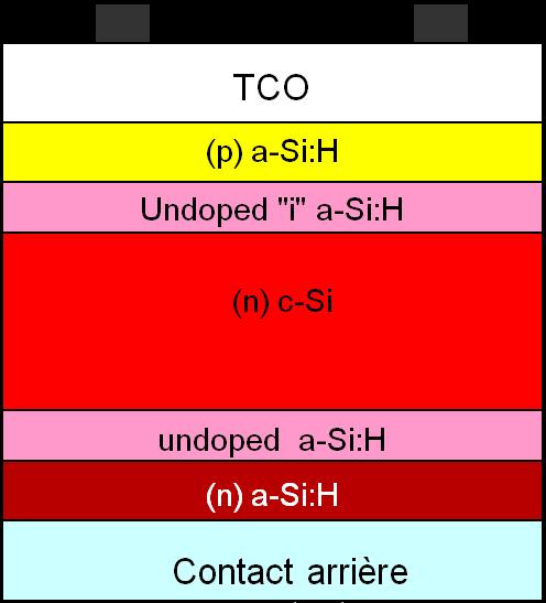
4 Illustration of the «HIT» solar cell Front Metal grid TCO (p) a-si:h Undoped "i" a-si:h (n) c-si 80 nm < 20 nm a-si:h/c-si solar cells «HIT» (Heterojunctions with Intrinsic Thin layers) : > 20%, V oc > 740 mv - Best efficiencies : 23,7% 100 µm Si wafers, Sanyo, > 21% on 125 cm 2 Si substrate, INES, HETSI project, (cf EPSEC 2011, Hambourg) How to reach high efficiencies? - low volume recombination B >>ms - low interface recombination s eff <<100 cm/s undoped a-si:h (n) a-si:h Back contact contact < 20 nm Fundamental and recurrent questions : - Surface Passivation mechanism? - Role of interface defects? - Band Lineup?
5 Measurement and analysis tools Quasi-Steady State Photoconductance (QSSPC) Microwave PhotoConductance Decay (µw-pcd) Passivation quality Photoluminescence (PL) Modulated Photoluminescence (MPL) Capacitance spectroscopy (C(V,f,T)) Interface band lineup Conductive Probe Atomic Force Microscopy (CP- AFM) Planar Conductance (G(T)) + Modelling and simulations
6 CP-AFM (Conductive Probe-AFM) applied to a-si:h/c-si Heterojunctions - Motivation - CP-AFM setup - Sample preparation - Experimental results - Comparison Experimental/Simulation Part 1


7 Motivation (n) a-si:h/ (p) c-si and (p) a- Si:H/ (n) c-si INTERFACES have been intensively studied by capacitance, planar conductance measurements, and modelling. ALL these studies suggest a STRONG INVERSION LAYER in c-si at the interface. CP-AFM is a powerful current sensing tool capable to probe directly interfaces


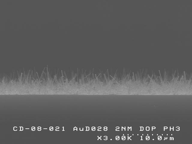
![bias [-10 V, 10 V], 0.](/docs-images/74/69812781/images/8-3.jpg "01 resolution Local")
8 CP-AFM setup - B-doped diamond tip : Radius curvature < 50 nm - Pt/Ir tip : Radius curvature < 25 nm DC bias [-10 V, 10 V], 0.01 resolution Local resistance range [ ]
 dip required to minimize surface oxide layer Cleavage Conductive AFM probe ITO a-si:h c-si ITO a-si:h i Bias V J.P.")

9 CP-AFM : Sample preparation - CP-AFM measurements performed on the heterojunction trench. - HF (1%) dip required to minimize surface oxide layer Cleavage Conductive AFM probe ITO a-si:h c-si ITO a-si:h i Bias V J.P. Kleider, J. Alvarez, A.V. Ankudinov, A. S. Gudovskikh, E.V. Gushina, M. Labrune, O. Maslova, W. Favre, M.E. Gueunier-Farret, P. Roca i Cabarrocas, E. I Terukov : "Characterization of silicon heterojunctions for solar cells", Nanoscale Research Letters 6:152 (2011), doi: / x-6-152
 c-si Electrical Image Conductive Channel : 2D-electron gas")
10 CP-AFM : Experimental results (1) Topographic image (n) a-si:h (p) c-si Electrical Image Conductive Channel : 2D-electron gas

11 CP-AFM : Experimental results (2) A B - A conductive channel is observed at the interface (n) a-si:h / (p) c-si which is more conductive than the bulk of c-si Strong inversion layer at the c-si surface. - 1 µm width region corresponding to the depletion region is also observed
12 CP-AFM : Comparison Experimental and Simulation - Resistivity profile calculations through AFORS-HET simulator confirm the quantitative CP-AFM measurements - Similar calculations on (p)a-si:h/(n)c-si reconfirms the existence of the strong inversion layer.
13 Silicon Nanowires Part 2 - Motivation -Vertical and horizontal silicon wire growth
14 Motivation L >1/α L >1/α a-si:h c-si Principle : Decoupling of light absorption and minority carrier collection Advantages : ħω Low production cost: - Lower silicon quality requirement - Low temperature deposition process (a-si:h) Tune wire dimensions 1 to promote absorption >L diff Efficiencies a-si:h/c-sinws based solar cell : Radial pn junction solar cell - 17 % conversion efficiency predicted % conversion efficiency demonstrated 3 (top-down approach) a-si:h c-si ħω >L diff [1] Kelzenberg et al, 33rd IEEE PVSC (2008) [2] Kelzenberg et al, Nature Mater. 9, (2010) [3] Y. Lu and A. Lal, Nano Lett. 10, (2010) Planar pn junction solar cell
.")

 1568 1571 Yu, L. and P. Roca i Cabarrocas, Physical Review B, 2010. 81(8): p. 085323 Yu, L., et al.")
15 Vertical and horizontal silicon wire growth - N-type SiNWs grown by CVD, Au-catalyzed VLS method, on (100) n++-type silicon substrates. Doping of SiNWs was achieved by adding PH 3 to SiH 4. - After growth, catalysts are removed + dopant activation annealing (RTA,750 C for 5 min). - In-Plane Solid-Liquid-Solid (IPSLS) technique uses In catalyst droplets and a hydrogenated amorphous silicon (a-si:h) layer to grow horizontal SiNWs. Growth activation is done during an annealing process in the range C. A-Si:H layer on top of ITO layer pattern 100 µm 2.1µm 440 nm In catalyst drop Region with only a-si:h covering - SiNWs embedded into SOG and planarized CMP S. Perraud et al. / Solar Energy Materials & Solar Cells 93 (2009) Yu, L. and P. Roca i Cabarrocas, Physical Review B, (8): p Yu, L., et al., Physical Review Letters, (12): p
16 Vertical SiNWs grown by VLS -CP-AFM analysis -Raman analysis


17 Electrical characterization of vertical/horizontal Si wires R AFMtip R Wcontact (a,, ) R SiNW R BackC Local resistance R Tot R AFMtip + R Wcontact (a,, ) + R SiNW + R BackC
 Topographic")


18 CP-AFM Analysis (1/3) Topographic image Electrical Image m 0 12 nm SiNWs brightest spots SiNWs blue spots
 R e s i s t")


19 CP-AFM Analysis (2/3) H e i g h t p r o f i l e ( n m ) R e s i s t a n c e p r o f i l e ( ) - [PH 3 ]/[SiH 4 ] drops local resistance by several orders of magnitude confirming the phosphorus incorporation. NEXT STEP Evaluation of the Resistivity & Phosphorus concentration
20 CP-AFM Analysis : Local I-V measurements (3/3) [PH 3 ]/[SiH 4 ] = 0 [PH 3 ]/[SiH 4 ] = [PH 3 ]/[SiH 4 ] = R Tot R AFMtip + R Wcontact (a,, ) + R SiNW + R BackC SiNW cm cm cm values versus [PH3]/[SiH4] are in good agreement with previous studies which employed 4-point probe measurements on single Si NWs 1-2. [P] = cm -3 [P] = cm -3 [P] = cm -3 [1] Eichfeld et al. Nanotechnology 18 (2007) [2] Wang et al. Nanoletters 5 (2005) 2139
21 Horizontal SiNWs grown by IPSLS -CP-AFM analysis -Raman analysis


 indicates trap-limited in SCLC => trap")
 higher surface/volume ratio and (ii) a-si:h (large DOS and")
: p.")
22 CP-AFM Analysis Si wires a-si:h In plane growth carried by a liquid catalyst drop advancing among a solid precursor. ITO pad Wire diameter and shapes are driven by : - initial hydrogen reduction of ITO - deformation of liquid catalyst drop during growth From the electrical point of view : - Local I-V measurements : n = 1.6 (V < 1 V) charge injection => Space-charge limited current n I V : n = 3 (V > 1 V) indicates trap-limited in SCLC => trap distribution Transport properties are driven by surface states : (i) higher surface/volume ratio and (ii) a-si:h (large DOS and exp. Tails) is the solid precursor used for the growth. Yu, L. and P. Roca i Cabarrocas, Physical Review B, (8): p Yu, L., et al., Physical Review Letters, (12): p


23 Raman Analysis (1) Solid precursor : a-si:h which is characterized by a large DOS in the gap with exp. tails. Structural quality of Si Wires? Confocal Raman analysis at 532 nm, 100X, pinhole size : 25 µm, P< 1mW, 600 g/mm Map of integrated Raman Signal [ cm -1 ]
24 Raman Analysis (2) Comparison SiNW Raman signal and c-si wafer (type N, 100, cm -3 ). 3.2 cm -1 In plane SiNW cm -1 FWHM 12 cm -1 c-si wafer cm -1 FWHM 4 cm -1 - In plane SiNW Raman shows a peak located 517 cm -1 with a FWHM 12 cm -1 Open questions : (i) Is tensile stress the origin of the shift? (ii) the wires are not c-si but µc-si:h or nc-si:h?
25 Conclusion Part 1 & Part 2 CP-AFM reveals itself as a powerful current sensing technique for the analysis of heterointerfaces, electrical transport properties and doping effect on SiNWs. Demonstrated the existence of a strong inversion layer (2D-carrier gas) in the c-si layer for both types of silicon heterojunctions. Evidenced the phosphorus incorporation and estimated the phosphorus concentration in vertical SiNWs. Evidenced of SCLC and trap-limited current transport properties in horizontal SiNWs surface states are the main ingredient controlling the transport properties.
 - C. Morin, S.")
26 Acknowledgments - M.E. Farret-Gueunier, I. Ngo, E. Blanc, D. Diouf, R. Varache W. Favre, P. Chrétien, O. Maslova (LGEP) - E. Gushina, A.V. Ankudinov, A.S Gudovskikh, E.I. Terukov (Ioffe Institute) - C. Morin, S. Perraud (CEA-Liten) - Symposium Organizers :
Characterization of silicon heterojunctions for solar cells
 NANO EXPRESS Open Access Characterization of silicon heterojunctions for solar cells Jean-Paul Kleider 1*, Jose Alvarez 1, Alexander Vitalievitch Ankudinov 2, Alexander Sergeevitch Gudovskikh 3, Ekaterina
High efficiency silicon and perovskite-silicon solar cells for electricity generation
 High efficiency silicon and perovskite-silicon solar cells for electricity generation Ali Dabirian Email: dabirian@ipm.ir 1 From Solar Energy to Electricity 2 Global accumulative PV installed In Iran it
Research Article Characterization of a-si:h/c-si Heterojunctions by Time Resolved Microwave Conductivity Technique
 Photoenergy, Article ID 304580, 4 pages http://dx.doi.org/10.1155/2014/304580 Research Article Characterization of a-si:h/c-si Heterojunctions by Time Resolved Microwave Conductivity Technique Amornrat
(Co-PIs-Mark Brongersma, Yi Cui, Shanhui Fan) Stanford University. GCEP Research Symposium 2013 Stanford, CA October 9, 2013
 Stanford University. GCEP Research Symposium 2013 Stanford, CA October 9, 2013") High-efficiency thin film nano-structured multi-junction solar James S. cells Harris (PI) (Co-PIs-Mark Brongersma, Yi Cui, Shanhui Fan) Stanford University GCEP Research Symposium 2013 Stanford, CA October
High-efficiency thin film nano-structured multi-junction solar James S. cells Harris (PI) (Co-PIs-Mark Brongersma, Yi Cui, Shanhui Fan) Stanford University GCEP Research Symposium 2013 Stanford, CA October
Novel High-Efficiency Crystalline-Si-Based Compound. Heterojunction Solar Cells: HCT (Heterojunction with Compound. Thin-layer)
") Electronic Supplementary Material (ESI) for Physical Chemistry Chemical Physics. This journal is the Owner Societies 2014 Supplementary Information for Novel High-Efficiency Crystalline-Si-Based Compound
Electronic Supplementary Material (ESI) for Physical Chemistry Chemical Physics. This journal is the Owner Societies 2014 Supplementary Information for Novel High-Efficiency Crystalline-Si-Based Compound
Supplementary Figure 1 XRD pattern of a defective TiO 2 thin film deposited on an FTO/glass substrate, along with an XRD pattern of bare FTO/glass
 Supplementary Figure 1 XRD pattern of a defective TiO 2 thin film deposited on an FTO/glass substrate, along with an XRD pattern of bare FTO/glass and a reference pattern of anatase TiO 2 (JSPDS No.: 21-1272).
Noncontact-AFM (nc-afm)
") Noncontact-AFM (nc-afm) Quantitative understanding of nc-afm A attractive interaction Δf Resonance frequency: f 0 Width of resonance curve (FWHM): Γ Γ+ΔΓ Γ Q-factor: Q π f Γ = 0 f 0 f Conservative forces
Noncontact-AFM (nc-afm) Quantitative understanding of nc-afm A attractive interaction Δf Resonance frequency: f 0 Width of resonance curve (FWHM): Γ Γ+ΔΓ Γ Q-factor: Q π f Γ = 0 f 0 f Conservative forces
Session 6: Solid State Physics. Diode
 Session 6: Solid State Physics Diode 1 Outline A B C D E F G H I J 2 Definitions / Assumptions Homojunction: the junction is between two regions of the same material Heterojunction: the junction is between
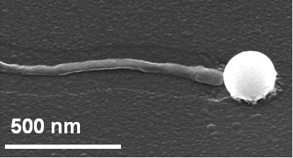
produced a sputter rate of 0.9 nm/s for the radially profiled, un-etched wires. A slightly
 Supporting Information: Beam Current and Sputtering Rate: Using a 16 kev Cs + primary ion beam and a 1 µm 2 rastered area, a 10 pa beam current produced a sputter rate of 0.9 nm/s for the radially profiled,
Photovoltaic cell and module physics and technology
 Photovoltaic cell and module physics and technology Vitezslav Benda, Prof Czech Technical University in Prague benda@fel.cvut.cz www.fel.cvut.cz 6/21/2012 1 Outlines Photovoltaic Effect Photovoltaic cell
Study of Silver Nanoparticles Electroless Growth and Their Impact on Silicon Properties
 Chemistry Journal Vol. 1, No. 3, 2015, pp. 90-94 http://www.publicscienceframework.org/journal/cj Study of Silver Nanoparticles Electroless Growth and Their Impact on Silicon Properties R. Benabderrahmane
Classification of Solids
 Classification of Solids Classification by conductivity, which is related to the band structure: (Filled bands are shown dark; D(E) = Density of states) Class Electron Density Density of States D(E) Examples
Solar Cell Materials and Device Characterization
 Solar Cell Materials and Device Characterization April 3, 2012 The University of Toledo, Department of Physics and Astronomy SSARE, PVIC Principles and Varieties of Solar Energy (PHYS 4400) and Fundamentals
Determination of localized conduction band-tail states distribution in single phase undoped microcrystalline silicon
 Determination of localized conduction band-tail states distribution in single ase undoped microcrystalline silicon Sanjay K. Ram *,a, Satyendra Kumar *,b and P. Roca i Cabarrocas! * Department of Physics
There's Plenty of Room at the Bottom
 There's Plenty of Room at the Bottom 12/29/1959 Feynman asked why not put the entire Encyclopedia Britannica (24 volumes) on a pin head (requires atomic scale recording). He proposed to use electron microscope
Temperature Dependent Current-voltage Characteristics of P- type Crystalline Silicon Solar Cells Fabricated Using Screenprinting
 Temperature Dependent Current-voltage Characteristics of P- type Crystalline Silicon Solar Cells Fabricated Using Screenprinting Process Hyun-Jin Song, Won-Ki Lee, Chel-Jong Choi* School of Semiconductor
SINCE the 1990s, asi:h/csi heterojunction solar cells have
 IEEE JOURNAL OF PHOTOVOLTAICS, VOL. 3, NO. 4, OCTOBER 2013 1149 Role of i-asi:h Layers in asi:h/csi Heterojunction Solar Cells Yutaka Hayashi, Member, IEEE, Debin Li, Atsushi Ogura, and Yoshio Ohshita
TEOS characterization of 2D materials from graphene to TMDCs
 Marc Chaigneau Yoshito Okuno, Andrey Krayev, Filippo Fabbri HORIBA Scientific AIST-NT Inc. IMEM-CNR Institute TEOS characterization of 2D materials from graphene to TMDCs 30-03-2017 Graphene2017 2015 2017
Lecture 1. OUTLINE Basic Semiconductor Physics. Reading: Chapter 2.1. Semiconductors Intrinsic (undoped) silicon Doping Carrier concentrations
 silicon Doping Carrier concentrations") Lecture 1 OUTLINE Basic Semiconductor Physics Semiconductors Intrinsic (undoped) silicon Doping Carrier concentrations Reading: Chapter 2.1 EE105 Fall 2007 Lecture 1, Slide 1 What is a Semiconductor? Low
Lecture 1 OUTLINE Basic Semiconductor Physics Semiconductors Intrinsic (undoped) silicon Doping Carrier concentrations Reading: Chapter 2.1 EE105 Fall 2007 Lecture 1, Slide 1 What is a Semiconductor? Low
Electrons are shared in covalent bonds between atoms of Si. A bound electron has the lowest energy state.
 Photovoltaics Basic Steps the generation of light-generated carriers; the collection of the light-generated carriers to generate a current; the generation of a large voltage across the solar cell; and
Photogating effect observed in microcrystalline silicon solar cells and its applications in cell optimization
 6 Photogating effect observed in microcrystalline silicon solar cells and its applications in cell optimization As we discussed in the previous Chapters, quantum efficiency measurement is of great importance
1 Name: Student number: DEPARTMENT OF PHYSICS AND PHYSICAL OCEANOGRAPHY MEMORIAL UNIVERSITY OF NEWFOUNDLAND. Fall :00-11:00
 1 Name: DEPARTMENT OF PHYSICS AND PHYSICAL OCEANOGRAPHY MEMORIAL UNIVERSITY OF NEWFOUNDLAND Final Exam Physics 3000 December 11, 2012 Fall 2012 9:00-11:00 INSTRUCTIONS: 1. Answer all seven (7) questions.
Toward a 1D Device Model Part 2: Material Fundamentals
 Toward a 1D Device Model Part 2: Material Fundamentals Lecture 8 10/4/2011 MIT Fundamentals of Photovoltaics 2.626/2.627 Fall 2011 Prof. Tonio Buonassisi 1 2.626/2.627 Roadmap You Are Here 2 2.626/2.627:
Graphene photodetectors with ultra-broadband and high responsivity at room temperature
 SUPPLEMENTARY INFORMATION DOI: 10.1038/NNANO.2014.31 Graphene photodetectors with ultra-broadband and high responsivity at room temperature Chang-Hua Liu 1, You-Chia Chang 2, Ted Norris 1.2* and Zhaohui
Diffusion in Extrinsic Silicon
 1 Diffusion in Extrinsic Silicon SFR Workshop & Review April 17, 2002 Hughes Silvestri, Ian Sharp, Hartmut Bracht, and Eugene Haller Berkeley, CA 2002 GOAL: Diffusion measurements on P doped Si to complete
Microwave Absorption by Light-induced Free Carriers in Silicon
 Microwave Asorption y Light-induced Free Carriers in Silicon T. Sameshima and T. Haa Tokyo University of Agriculture and Technology, Koganei, Tokyo 184-8588, Japan E-mail address: tsamesim@cc.tuat.ac.jp
Repo, Päivikki & Talvitie, Heli & Li, Shuo & Skarp, Jarmo & Savin, Hele Silicon Surface Passivation by Al2O3: Effect of ALD Reactants
 Powered by TCPDF (www.tcpdf.org) This is an electronic reprint of the original article. This reprint may differ from the original in pagination and typographic detail. Author(s): Title: Repo, Päivikki
Photovoltaic cell and module physics and technology. Vitezslav Benda, Prof Czech Technical University in Prague
 Photovoltaic cell and module physics and technology Vitezslav Benda, Prof Czech Technical University in Prague benda@fel.cvut.cz www.fel.cvut.cz 1 Outlines Photovoltaic Effect Photovoltaic cell structure
Semiconductor X-Ray Detectors. Tobias Eggert Ketek GmbH
 Semiconductor X-Ray Detectors Tobias Eggert Ketek GmbH Semiconductor X-Ray Detectors Part A Principles of Semiconductor Detectors 1. Basic Principles 2. Typical Applications 3. Planar Technology 4. Read-out
CITY UNIVERSITY OF HONG KONG. Theoretical Study of Electronic and Electrical Properties of Silicon Nanowires
 CITY UNIVERSITY OF HONG KONG Ë Theoretical Study of Electronic and Electrical Properties of Silicon Nanowires u Ä öä ªqk u{ Submitted to Department of Physics and Materials Science gkö y in Partial Fulfillment
Carbon Nanomaterials
 Carbon Nanomaterials STM Image 7 nm AFM Image Fullerenes C 60 was established by mass spectrographic analysis by Kroto and Smalley in 1985 C 60 is called a buckminsterfullerene or buckyball due to resemblance
HETEROJUNCTION with intrinsic thin-layer (HIT) solar
 solar") IEEE TRANSACTIONS ON ELECTRON DEVICES, VOL. 59, NO. 5, MAY 2012 1227 Mechanism of Trapping Effect in Heterojunction With Intrinsic Thin-Layer Solar Cells: Effect of Density of Defect States X. Hua, Z.
IEEE TRANSACTIONS ON ELECTRON DEVICES, VOL. 59, NO. 5, MAY 2012 1227 Mechanism of Trapping Effect in Heterojunction With Intrinsic Thin-Layer Solar Cells: Effect of Density of Defect States X. Hua, Z.
OPTO-ELECTRONIC MODELLING OF THIN FILM NANOCRYSTALLINE SILICON SOLAR CELLS
 Journal of Ovonic Research Vol. 8, No. 4, July - August 2012, p. 81-90 OPTO-ELECTRONIC MODELLING OF THIN FILM NANOCRYSTALLINE SILICON SOLAR CELLS S.N. AGBO a, P.E. UGWUOKE a, F.I. EZEMA b a National Centre
Infrared Charge-Modulation Spectroscopy of Defects in Phosphorus Doped Amorphous Silicon
 Syracuse University SURFACE Physics College of Arts and Sciences 22 Infrared Charge-Modulation Spectroscopy of Defects in Phosphorus Doped Amorphous Silicon Kai Zhu Syracuse University Eric A. Schiff Syracuse
Semiconductor Physics fall 2012 problems
 Semiconductor Physics fall 2012 problems 1. An n-type sample of silicon has a uniform density N D = 10 16 atoms cm -3 of arsenic, and a p-type silicon sample has N A = 10 15 atoms cm -3 of boron. For each
Review of Semiconductor Fundamentals
 ECE 541/ME 541 Microelectronic Fabrication Techniques Review of Semiconductor Fundamentals Zheng Yang (ERF 3017, email: yangzhen@uic.edu) Page 1 Semiconductor A semiconductor is an almost insulating material,
D DAVID PUBLISHING. Study the Synthesis Parameter of Tin Oxide Nanostructure. 1. Introduction. 2. Experiment
 Journal of Materials Science and Engineering B 5 (9-10) (2015) 353-360 doi: 10.17265/2161-6221/2015.9-10.003 D DAVID PUBLISHING Study the Synthesis Parameter of Tin Oxide Nanostructure Gyanendra Prakash
Extrinsic Origin of Persistent Photoconductivity in
 Supporting Information Extrinsic Origin of Persistent Photoconductivity in Monolayer MoS2 Field Effect Transistors Yueh-Chun Wu 1, Cheng-Hua Liu 1,2, Shao-Yu Chen 1, Fu-Yu Shih 1,2, Po-Hsun Ho 3, Chun-Wei
Low temperature anodically grown silicon dioxide films for solar cell. Nicholas E. Grant
 Low temperature anodically grown silicon dioxide films for solar cell applications Nicholas E. Grant Outline 1. Electrochemical cell design and properties. 2. Direct-current current anodic oxidations-part
Semiconductor Junctions
 8 Semiconductor Junctions Almost all solar cells contain junctions between different materials of different doping. Since these junctions are crucial to the operation of the solar cell, we will discuss
Semiconductor Nanowires: Motivation
 Semiconductor Nanowires: Motivation Patterning into sub 50 nm range is difficult with optical lithography. Self-organized growth of nanowires enables 2D confinement of carriers with large splitting of
Supplementary Figure 1. Supplementary Figure 1 Characterization of another locally gated PN junction based on boron
 Supplementary Figure 1 Supplementary Figure 1 Characterization of another locally gated PN junction based on boron nitride and few-layer black phosphorus (device S1). (a) Optical micrograph of device S1.
Diffusion in Extrinsic Silicon and Silicon Germanium
 1 Diffusion in Extrinsic Silicon and Silicon Germanium SFR Workshop & Review November 14, 2002 Hughes Silvestri, Ian Sharp, Hartmut Bracht, and Eugene Haller Berkeley, CA 2002 GOAL: Diffusion measurements
Nanostrukturphysik (Nanostructure Physics)
") Nanostrukturphysik (Nanostructure Physics) Prof. Yong Lei & Dr. Yang Xu Fachgebiet 3D-Nanostrukturierung, Institut für Physik Contact: yong.lei@tu-ilmenau.de; yang.xu@tu-ilmenau.de Office: Unterpoerlitzer
Nanostrukturphysik (Nanostructure Physics) Prof. Yong Lei & Dr. Yang Xu Fachgebiet 3D-Nanostrukturierung, Institut für Physik Contact: yong.lei@tu-ilmenau.de; yang.xu@tu-ilmenau.de Office: Unterpoerlitzer
The Role of Hydrogen in Defining the n-type Character of BiVO 4 Photoanodes
 Supporting Information The Role of Hydrogen in Defining the n-type Character of BiVO 4 Photoanodes Jason K. Cooper, a,b Soren B. Scott, a Yichuan Ling, c Jinhui Yang, a,b Sijie Hao, d Yat Li, c Francesca
Final Examination EE 130 December 16, 1997 Time allotted: 180 minutes
 Final Examination EE 130 December 16, 1997 Time allotted: 180 minutes Problem 1: Semiconductor Fundamentals [30 points] A uniformly doped silicon sample of length 100µm and cross-sectional area 100µm 2
CHARACTERIZATION OF FUNDAMENTAL PARAMETERS OF FRONT JUNCTION AMORPHOUS/CRYSTALLINE SILICON HETEROJUNCTION SOLAR CELLS USING VARIOUS ELECTRICAL METHODS
 CHARACTERIZATION OF FUNDAMENTAL PARAMETERS OF FRONT JUNCTION AMORPHOUS/CRYSTALLINE SILICON HETEROJUNCTION SOLAR CELLS USING VARIOUS ELECTRICAL METHODS by Swapna Mudigonda A thesis submitted to the Faculty
Chalcogenide semiconductor research and applications. Tutorial 2: Thin film characterization. Rafael Jaramillo Massachusetts Institute of Technology
 Chalcogenide semiconductor research and applications Tutorial 2: Thin film characterization Rafael Jaramillo Massachusetts Institute of Technology Section 1: Measuring composition August 20, 2017 Jaramillo
Quiz #1 Practice Problem Set
 Name: Student Number: ELEC 3908 Physical Electronics Quiz #1 Practice Problem Set? Minutes January 22, 2016 - No aids except a non-programmable calculator - All questions must be answered - All questions
Dark Current Limiting Mechanisms in CMOS Image Sensors
 Dark Current Limiting Mechanisms in CMOS Image Sensors Dan McGrath BAE Systems Information and Electronic Systems Integration Inc., Lexington, MA 02421, USA,
R. Ludwig and G. Bogdanov RF Circuit Design: Theory and Applications 2 nd edition. Figures for Chapter 6
 R. Ludwig and G. Bogdanov RF Circuit Design: Theory and Applications 2 nd edition Figures for Chapter 6 Free electron Conduction band Hole W g W C Forbidden Band or Bandgap W V Electron energy Hole Valence
Research Article Modeling and Optimization of Advanced Single- and Multijunction Solar Cells Based on Thin-Film a-si:h/sige Heterostructure
 International Scholarly Research Network ISRN Renewable Energy Volume 211, Article ID 712872, 8 pages doi:1.542/211/712872 Research Article Modeling and Optimization of Advanced Single- and Multijunction
Chapter 7. Solar Cell
 Chapter 7 Solar Cell 7.0 Introduction Solar cells are useful for both space and terrestrial application. Solar cells furnish the long duration power supply for satellites. It converts sunlight directly
CVD: General considerations.
 CVD: General considerations. PVD: Move material from bulk to thin film form. Limited primarily to metals or simple materials. Limited by thermal stability/vapor pressure considerations. Typically requires
Xing Sheng, 微纳光电子材料与器件工艺原理. Doping 掺杂. Xing Sheng 盛兴. Department of Electronic Engineering Tsinghua University
 微纳光电子材料与器件工艺原理 Doping 掺杂 Xing Sheng 盛兴 Department of Electronic Engineering Tsinghua University xingsheng@tsinghua.edu.cn 1 Semiconductor PN Junctions Xing Sheng, EE@Tsinghua LEDs lasers detectors solar
Supplementary Figure 1 Experimental setup for crystal growth. Schematic drawing of the experimental setup for C 8 -BTBT crystal growth.
 Supplementary Figure 1 Experimental setup for crystal growth. Schematic drawing of the experimental setup for C 8 -BTBT crystal growth. Supplementary Figure 2 AFM study of the C 8 -BTBT crystal growth
FYS 3028/8028 Solar Energy and Energy Storage. Calculator with empty memory Language dictionaries
 Faculty of Science and Technology Exam in: FYS 3028/8028 Solar Energy and Energy Storage Date: 11.05.2016 Time: 9-13 Place: Åsgårdvegen 9 Approved aids: Type of sheets (sqares/lines): Number of pages incl.
CVD-3 LFSIN SiN x Process
 CVD-3 LFSIN SiN x Process Top Electrode, C Bottom Electrode, C Pump to Base Time (s) SiH 4 Flow Standard LFSIN Process NH 3 Flow N 2 HF (watts) LF (watts) Pressure (mtorr Deposition Time min:s.s Pump to
Recap (so far) Low-Dimensional & Boundary Effects
 Low-Dimensional & Boundary Effects") Recap (so far) Ohm s & Fourier s Laws Mobility & Thermal Conductivity Heat Capacity Wiedemann-Franz Relationship Size Effects and Breakdown of Classical Laws 1 Low-Dimensional & Boundary Effects Energy
Recap (so far) Ohm s & Fourier s Laws Mobility & Thermal Conductivity Heat Capacity Wiedemann-Franz Relationship Size Effects and Breakdown of Classical Laws 1 Low-Dimensional & Boundary Effects Energy
ET3034TUx Utilization of band gap energy
 ET3034TUx - 3.3.1 - Utilization of band gap energy In the last two weeks we have discussed the working principle of a solar cell and the external parameters that define the performance of a solar cell.
CVD-3 MFSIN-HU-1 SiN x Mixed Frequency Process
 CVD-3 MFSIN-HU-1 SiN x Mixed Frequency Process Standard MFSIN-HU-1 Process Top C Bottom C Pump to Base Time (s) SiH 4 Flow HF/ LF NH 3 Flow HF/LF N 2 HF/LF HF (watts) LF (watts) HF Time LF Time Pressure
Greg Andreev and Aravind Vijayaraghavan 9/27/13
 Mapping Graphene s surface potential with
Development and application for X-ray excited optical luminescence (XEOL) technology at STXM beamline of SSRF
 technology at STXM beamline of SSRF") Development and application for X-ray excited optical luminescence (XEOL) technology at STXM beamline of SSRF Content Introduction to XEOL Application of XEOL Development and Application of XEOL in STXM
Development and application for X-ray excited optical luminescence (XEOL) technology at STXM beamline of SSRF Content Introduction to XEOL Application of XEOL Development and Application of XEOL in STXM
The pn junction. [Fonstad, Ghione]
![The pn junction. [Fonstad, Ghione]](/thumbs/93/112370833.jpg "The pn junction. [Fonstad, Ghione]") The pn junction [Fonstad, Ghione] Band diagram On the vertical axis: potential energy of the electrons On the horizontal axis: now there is nothing: later we ll put the position qf s : work function (F
The pn junction [Fonstad, Ghione] Band diagram On the vertical axis: potential energy of the electrons On the horizontal axis: now there is nothing: later we ll put the position qf s : work function (F
SEMICONDUCTOR MATERIAL AND DEVICE CHARACTERIZATION
 SEMICONDUCTOR MATERIAL AND DEVICE CHARACTERIZATION SEMICONDUCTOR MATERIAL AND DEVICE CHARACTERIZATION Third Edition DIETER K. SCHRODER Arizona State University Tempe, AZ A JOHN WILEY & SONS, INC., PUBLICATION
High efficiency solar cells by nanophotonic design
 High efficiency solar cells by nanophotonic design Piero Spinelli Claire van Lare Jorik van de Groep Bonna Newman Mark Knight Paula Bronsveld Frank Lenzmann Ruud Schropp Wim Sinke Albert Polman Center
(a) (b) Supplementary Figure 1. (a) (b) (a) Supplementary Figure 2. (a) (b) (c) (d) (e)
 (b) Supplementary Figure 1. (a) (b) (a) Supplementary Figure 2. (a) (b) (c) (d) (e)") (a) (b) Supplementary Figure 1. (a) An AFM image of the device after the formation of the contact electrodes and the top gate dielectric Al 2 O 3. (b) A line scan performed along the white dashed line
(a) (b) Supplementary Figure 1. (a) An AFM image of the device after the formation of the contact electrodes and the top gate dielectric Al 2 O 3. (b) A line scan performed along the white dashed line
Analysis of the Temperature Dependence of the Open-Circuit Voltage
 Vailable online at www.sciencedirect.com Energy Procedia 27 (212 ) 135 142 SiliconPV: April 3-5, 212, Leuven, Belgium Analysis of the Temperature Dependence of the Open-Circuit Voltage P. Löper a,c *,
Three-Dimensional Silicon-Germanium Nanostructures for Light Emitters and On-Chip Optical. Interconnects
 Three-Dimensional Silicon-Germanium Nanostructures for Light Emitters and On-Chip Optical eptember 2011 Interconnects Leonid Tsybeskov Department of Electrical and Computer Engineering New Jersey Institute
Spin Dynamics in Single GaAs Nanowires
 1 Dr. Max Mustermann Referat Kommunikation & Marketing Verwaltung Spin Dynamics in Single GaAs Nanowires F. Dirnberger, S. Furthmeier, M. Forsch, A. Bayer, J. Hubmann, B. Bauer, J. Zweck, E. Reiger, C.
SUPPLEMENTARY INFORMATION
 doi:.38/nature09979 I. Graphene material growth and transistor fabrication Top-gated graphene RF transistors were fabricated based on chemical vapor deposition (CVD) grown graphene on copper (Cu). Cu foil
SUPPLEMENTARY INFORMATION
 DOI: 10.1038/NCHEM.1332 Light triggered self-construction of supramolecular organic nanowires as metallic interconnects Vina Faramarzi 1,2, Frédéric Niess 1,3, Emilie Moulin 3, Mounir Maaloum 1,3, Jean-François
PHOTOVOLTAICS Fundamentals
 PHOTOVOLTAICS Fundamentals PV FUNDAMENTALS Semiconductor basics pn junction Solar cell operation Design of silicon solar cell SEMICONDUCTOR BASICS Allowed energy bands Valence and conduction band Fermi
Sheng S. Li. Semiconductor Physical Electronics. Second Edition. With 230 Figures. 4) Springer
 Springer") Sheng S. Li Semiconductor Physical Electronics Second Edition With 230 Figures 4) Springer Contents Preface 1. Classification of Solids and Crystal Structure 1 1.1 Introduction 1 1.2 The Bravais Lattice
Sheng S. Li Semiconductor Physical Electronics Second Edition With 230 Figures 4) Springer Contents Preface 1. Classification of Solids and Crystal Structure 1 1.1 Introduction 1 1.2 The Bravais Lattice
Surface Transfer Doping of Diamond by Organic Molecules
 Surface Transfer Doping of Diamond by Organic Molecules Qi Dongchen Department of Physics National University of Singapore Supervisor: Prof. Andrew T. S. Wee Dr. Gao Xingyu Scope of presentation Overview
KATIHAL FİZİĞİ MNT-510
 KATIHAL FİZİĞİ MNT-510 YARIİLETKENLER Kaynaklar: Katıhal Fiziği, Prof. Dr. Mustafa Dikici, Seçkin Yayıncılık Katıhal Fiziği, Şakir Aydoğan, Nobel Yayıncılık, Physics for Computer Science Students: With
CARBON NANOSTRUCTURES SYNTHESIZED THROUGH GRAPHITE ETCHING
 CARBON NANOSTRUCTURES SYNTHESIZED THROUGH GRAPHITE ETCHING Q. Yang 1, C. Xiao 1, R. Sammynaiken 2 and A. Hirose 1 1 Plasma Physics Laboratory, University of Saskatchewan, 116 Science Place Saskatoon, SK
How a single defect can affect silicon nano-devices. Ted Thorbeck
 How a single defect can affect silicon nano-devices Ted Thorbeck tedt@nist.gov The Big Idea As MOS-FETs continue to shrink, single atomic scale defects are beginning to affect device performance Gate Source
Supplementary Figure 1 Interlayer exciton PL peak position and heterostructure twisting angle. a, Photoluminescence from the interlayer exciton for
 Supplementary Figure 1 Interlayer exciton PL peak position and heterostructure twisting angle. a, Photoluminescence from the interlayer exciton for six WSe 2 -MoSe 2 heterostructures under cw laser excitation
Optical properties of nano-silicon
 Bull. Mater. Sci., Vol. 4, No. 3, June 001, pp. 85 89. Indian Academy of Sciences. Optical properties of nano-silicon S TRIPATHY, R K SONI*, S K GHOSHAL and K P JAIN Department of Physics, Indian Institute
Transparent Electrode Applications
 Transparent Electrode Applications LCD Solar Cells Touch Screen Indium Tin Oxide (ITO) Zinc Oxide (ZnO) - High conductivity - High transparency - Resistant to environmental effects - Rare material (Indium)
Nanostructured Inorganic Solar Cells
 Green, Vol. 1 (2011), pp. 7 27 Copyright 2011 De Gruyter. DOI 10.1515/GREEN.2011.007 Review Nanostructured Inorganic Solar Cells Kevin P. Musselman 1; and Lukas Schmidt-Mende 2 1 Department of Physics,
UNIVERSITY OF CALIFORNIA College of Engineering Department of Electrical Engineering and Computer Sciences. Professor Chenming Hu.
 UNIVERSITY OF CALIFORNIA College of Engineering Department of Electrical Engineering and Computer Sciences EECS 130 Spring 2009 Professor Chenming Hu Midterm I Name: Closed book. One sheet of notes is
Formation of Nanostructured Layers for Passivation of High Power Silicon Devices
 Vol. 113 (2008) ACTA PHYSICA POLONICA A No. 3 Proceedings of the 13th International Symposium UFPS, Vilnius, Lithuania 2007 Formation of Nanostructured Layers for Passivation of High Power Silicon Devices
Holes (10x larger). Diode currents proportional to minority carrier densities on each side of the depletion region: J n n p0 = n i 2
. Diode currents proportional to minority carrier densities on each side of the depletion region: J n n p0 = n i 2") Part V. (40 pts.) A diode is composed of an abrupt PN junction with N D = 10 16 /cm 3 and N A =10 17 /cm 3. The diode is very long so you can assume the ends are at x =positive and negative infinity. 1.
Part V. (40 pts.) A diode is composed of an abrupt PN junction with N D = 10 16 /cm 3 and N A =10 17 /cm 3. The diode is very long so you can assume the ends are at x =positive and negative infinity. 1.
UNIVERSITY OF CALIFORNIA College of Engineering Department of Electrical Engineering and Computer Sciences. EECS 130 Professor Ali Javey Fall 2006
 UNIVERSITY OF CALIFORNIA College of Engineering Department of Electrical Engineering and Computer Sciences EECS 130 Professor Ali Javey Fall 2006 Midterm 2 Name: SID: Closed book. Two sheets of notes are
CONTROL AND OPTIMIZATION OF THERMAL OXIDATION PROCESSES FOR INDUSTRIAL SOLAR CELL FABRICATION S (1)
") CONTROL AND OPTIMIZATION OF THERMAL OXIDATION PROCESSES FOR INDUSTRIAL SOLAR CELL FABRICATION Sebastian Mack, Anke Lemke, Andreas Wolf, Benedikt Holzinger, Martin Zimmer, Daniel Biro, and Ralf Preu Fraunhofer
CONTROL AND OPTIMIZATION OF THERMAL OXIDATION PROCESSES FOR INDUSTRIAL SOLAR CELL FABRICATION Sebastian Mack, Anke Lemke, Andreas Wolf, Benedikt Holzinger, Martin Zimmer, Daniel Biro, and Ralf Preu Fraunhofer
UNIVERSITY OF CALIFORNIA College of Engineering Department of Electrical Engineering and Computer Sciences. EECS 130 Professor Ali Javey Fall 2006
 UNIVERSITY OF CALIFORNIA College of Engineering Department of Electrical Engineering and Computer Sciences EECS 130 Professor Ali Javey Fall 2006 Midterm I Name: Closed book. One sheet of notes is allowed.
Characterization of Irradiated Doping Profiles. Wolfgang Treberspurg, Thomas Bergauer, Marko Dragicevic, Manfred Krammer, Manfred Valentan
 Characterization of Irradiated Doping Profiles, Thomas Bergauer, Marko Dragicevic, Manfred Krammer, Manfred Valentan Vienna Conference on Instrumentation (VCI) 14.02.2013 14.02.2013 2 Content: Experimental
New experimental evidence for the role of long- range potential fluctuations in the mechanism of 1/f noise in a-si:h
 New experimental evidence for the role of long- range potential fluctuations in the mechanism of 1/f noise in a-si:h J.P.R. Bakker 1, P.J.S. van Capel 1, B.V. Fine 2,3, and J.I. Dijkhuis 1 1 Debye Institute
Modelling of Diamond Devices with TCAD Tools
 RADFAC Day - 26 March 2015 Modelling of Diamond Devices with TCAD Tools A. Morozzi (1,2), D. Passeri (1,2), L. Servoli (2), K. Kanxheri (2), S. Lagomarsino (3), S. Sciortino (3) (1) Engineering Department
Thermal Oxidation of Si
 Thermal Oxidation of General Properties of O 2 Applications of thermal O 2 Deal-Grove Model of Oxidation Thermal O 2 is amorphous. Weight Density = 2.20 gm/cm 3 Molecular Density = 2.3E22 molecules/cm
Repo, Päivikki; Talvitie, Heli; Li, Shuo; Skarp, Jarmo; Savin, Hele Silicon Surface Passivation by Al2O3: Effect of ALD Reactants
 Powered by TCPDF (www.tcpdf.org) This is an electronic reprint of the original article. This reprint may differ from the original in pagination and typographic detail. Repo, Päivikki; Talvitie, Heli; Li,
The interfacial study on the Cu 2 O/Ga 2 O 3 /AZO/TiO 2 photocathode for water splitting fabricated by pulsed laser deposition
 Electronic Supplementary Material (ESI) for Catalysis Science & Technology. This journal is The Royal Society of Chemistry 2017 The interfacial study on the Cu 2 O/Ga 2 O 3 /AZO/TiO 2 photocathode for
CVD-3 SIO-HU SiO 2 Process
 CVD-3 SIO-HU SiO 2 Process Top Electrode, C Bottom Electrode, C Pump to Base Time (s) SiH 4 Flow Standard SIO-HU Process N 2 O Flow N 2 HF (watts) LF (watts) Pressure (mtorr Deposition Time min:s.s Pump
vapour deposition. Raman peaks of the monolayer sample grown by chemical vapour
 Supplementary Figure 1 Raman spectrum of monolayer MoS 2 grown by chemical vapour deposition. Raman peaks of the monolayer sample grown by chemical vapour deposition (S-CVD) are peak which is at 385 cm
MENA9510 characterization course: Capacitance-voltage (CV) measurements
 measurements") MENA9510 characterization course: Capacitance-voltage (CV) measurements 30.10.2017 Halvard Haug Outline Overview of interesting sample structures Ohmic and schottky contacts Why C-V for solar cells? The
MENA9510 characterization course: Capacitance-voltage (CV) measurements 30.10.2017 Halvard Haug Outline Overview of interesting sample structures Ohmic and schottky contacts Why C-V for solar cells? The
Lecture 18. New gas detectors Solid state trackers
 Lecture 18 New gas detectors Solid state trackers Time projection Chamber Full 3-D track reconstruction x-y from wires and segmented cathode of MWPC z from drift time de/dx information (extra) Drift over
Photoelectrochemical characterization of Bi 2 S 3 thin films deposited by modified chemical bath deposition
 Indian Journal of Engineering & Materials Sciences Vol. 13, April; 2006, pp. 140-144 Photoelectrochemical characterization of Bi 2 S 3 thin films deposited by modified chemical bath deposition R R Ahire
Device 3D. 3D Device Simulator. Nano Scale Devices. Fin FET
 Device 3D 3D Device Simulator Device 3D is a physics based 3D device simulator for any device type and includes material properties for the commonly used semiconductor materials in use today. The physical