EU: NANOMOL-CANEL. Bottom-up opportunities - the promise of molecular electronics. Thomas Bjørnholm, Nano-Science Center, University of Copenhagen
|
|
|
- Stephanie Franklin
- 5 years ago
- Views:
Transcription


. Kasper Nørgård, Thomas Bjørnholm Chem.")
1 Bottom-up opportunities - the promise of molecular electronics Thomas Bjørnholm, Nano-cience Center, University of Copenhagen EU: NANOMOL-CANEL INGLE ELECTRON TRANITOR OF A INGLE CONJUGATED MOLECULE WITH ACCE TO EVERAL REDOX TATE ergey Kubatkin, Andrey Danilov, Mattias Hjort, Jérôme Cornil, Jean-Luc Brédas, Nicolai tuhr-hansen, Per Hedegård, and Thomas Bjørnholm Nature, (2003). Kasper Nørgård, Thomas Bjørnholm Chem. Commun. Feature 1793 (2005) Artist view

2 Background: Two-terminal devices (diodes) H - H TM BrJ H π H Gold electrode Aviram & Ratner: ingle molecule diode (in theory)

3 Background: Three-terminal devices (field effect transistors) R (ΓG 0 ) -1 V sd V g R ource Q R Drain Q D D D Q Q Energy Gate R GΩ, Q = ne equential electron transfer R kω, Q 0 Tunneling V sd current V sd no current current no current V g Current V g
 R Q R V sd Q1 Q1 ource")

4 Background: Three-terminal devices (field effect transistors) R Q R V sd Q1 Q1 ource Drain V g Gate V sd 3 nm V g Classical Coulomb charging dominates large nanostructures
 Easy to tailor make all alike; (2) flexible (responsive); (3) easy to process from solution; (4) self-organize;")
5 Organic molecules are great. We are made of them! (1) Easy to tailor make all alike; (2) flexible (responsive); (3) easy to process from solution; (4) self-organize; (stability (auto repair)) H n N 1 nm N N Co 2+/3+ n n n N N N H n
6 ynthesis of efficient building blocks for self-assembling electronics CHO R OHC R 1) CH 3 COCl/ BBr 3 /CH 2 Cl 2 2) I 2 /Toluene O R O all trans OPV5 Nicolai tuhr Hansen J. Org. Chem. 68, (2003).
7 Fabrication of the ET 3.2 nm 2 nm CVD T = 4 K ergey Kubatkin Nature, (2003).
8 ingle molecule single electron transistor 2 nm Nature, (2003).


9 ingle molecule single electron transistor R GΩ, Q = ne equential electron transfer V sd current no current no current V g current V sd 300 mev V g
10 EC: J. Heinze, K. Müllen, et al, J. Chem. oc. Chem. Commun Ι(n n+1) = μ OPV (n+1, 0) μ OPV (n, 0) = (C g /(C s +C d +C g ) )e ( V g (n) - V g (n+1)) Redox chemistry in the ET R 5 GΩ
11 ummary of ET results HOMO - LUMO GAP

12 -1 Al 2 O mev mev mev mev
 4eV E (ev) Per Hedegaard Hubbard model: t = 3.92 ev, U = 4.27 ev, aε r = 4.7 Å Chem. Phys.")
13 Molecule and device are not separable due to strong image charge effects δ(α) = 27.2 evå/(4 Å * ε r ) 4eV E (ev) Per Hedegaard Hubbard model: t = 3.92 ev, U = 4.27 ev, aε r = 4.7 Å Chem. Phys. in press (2005), Cond. Mat. 2005
14

15 tructure model of the ET of OPV5

16 Zoom on image charge
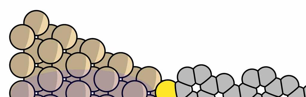
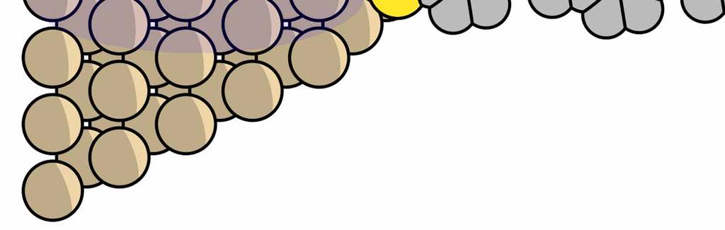
17 Prediction for chemisorbed OPV
18 ynthesis of efficient building blocks for self-assembling electronics CHO R OHC R 1) CH 3 COCl/ BBr 3 /CH 2 Cl 2 2) I 2 /Toluene O R O all trans OPV5 Nicolai tuhr Hansen J. Org. Chem. 68, (2003).
19 TEM of electromigration QuickTime and a Cinepak decompressor are needed to see this picture. QuickTime and a Cinepak decompressor are needed to see this picture. H.B. Heersche, G. Lientschnig, H.W. Zandbergen and H.J. van der Zant (to be published).
 2 0-2 boomerang I")
 -2-500 0 500 Vb (mv) -2000-500 0 500 Vb (mv) -3-50 0")
20 Breaking process with and without molecules Molecules self assemble on the gold electrodes prior to breaking bare gold OPV3 I (na) boomerang I (na) CB I (na) tunnel I (na) steps Vb (mv) Vb (mv) Vb (mv) Vb (mv)
 0.15 0.10 0.")
21 Controls with solvent only 20 T =4.2 K 10 I (na) Vb (mv) 0.20 Large Kondo temperatures and in general very little gate dependence! diff. cond. (μ) T k = 500 K Vb (mv)
22 Molecular junction with OPV-3: Kondo I (na) peak height (μ) 10 5 T k 20 K peak height (e 2 /h) T (K) Vb (mv) weak gate dependence diff. conductance (μ) diff. conductance (e 2 /h) V bias (mv) Vb (mv) Herre van der Zant unpub. V gate (V)
 QuickTime and a TIFF (LZW) decompressor are needed to see this picture.")
 5.2x10⁻³ 4.5x10⁻³ 3.")
 V gate (V) Diff. Cond.")
23 Another molecular junction with OPV-3: Kondo? V bias (mv) QuickTime and a TIFF (LZW) decompressor are needed to see this picture. B = 0 NDR spin blockade? B = 7T Diff. Cond. (n) K 2.7K 3K 3.5K 4K 4.5K 5K 5.5K 6K 6.5K T-dependence T k 12 K x Vb (mv) 5.2x x x x x10-3 Diff. Cond. (e 2 /h) V gate (V) Diff. Cond. (n) Herre van der Zant unpub. g = 3.4 V gate (V) B-dependence Vb (mv) Diff. Cond. (e 2 /h)
 0-50 -100-150 -15-10 -5 0 5 10 15 Vb (mv) na")
24 Relation between molecular properties and charge transport H π H H π H R/Ω H H H H I (na) Vb (mv) na pa
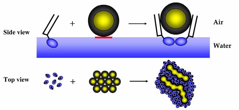
25 MEMPHY LOGO, Tegning af O. B. ørensen Proof of concept

26 Nature (2000)


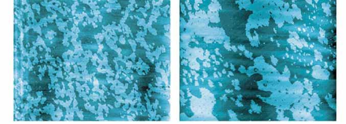
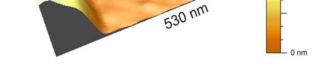
27 AFM topgraphy of DPPC + Au-nanoparticles b + 25 μm 50 μm Adv. Mat. 14, (2002).
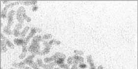
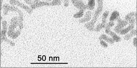
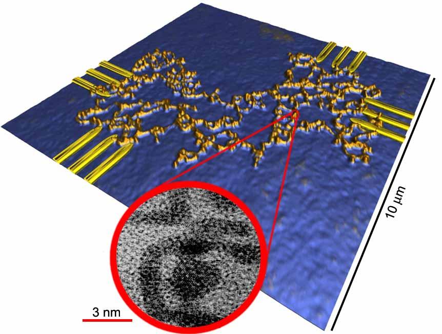
28 TEM 3 nm Tue Hassenkam/Kasper Nørgård Adv. Mat. 14, (2002).


29 LIPID Nano Letters 4, (2004)


30 LIPID Nano Letters 4, (2004).
31 Nano Letters 4, (2004).

32 QuickTime and a TIFF (LZW) decompressor are needed to see this picture. QuickTime and a TIFF (LZW) decompressor are needed to see this picture. QuickTime and a TIFF (LZW) decompressor are needed to see this picture. 3 nm Adv. Mat. 14, (2002).
33


34 Molecular memory devices of Langmuir films of Rotaxanes (Collaboration with Fraser toddart et al) -2e - + 2e - ++ olution: Yes olid state (film):?
35
36
37
38 Nano-imaging
39
40 QuickTime and a TIFF (LZW) decompressor are needed to see this picture.
-komprimeringsværktøj,")
41 Rotaxane status -2e - + 2e - ++? Der kræves QuickTime og et TIFF (LZW)-komprimeringsværktøj, for at man kan se dette billede.
42 Acknowledgements Herre van der Zant, Delft INGLE ELECTRON TRANPORT THROUGH A INGLE CONJUGATED MOLECULE ergey Kubatkin, Andrey Danilov, Mattias Hjort, Jérôme Cornil, Jean-Luc Brédas, Nicolai tuhr-hansen, Per Hedegård, Thomas Bjørnholm Nature, (2003). ELF-AEMBLY AND CONDUCTIVE PROPERTIE OF MOLECULARLY LINKED GOLD NANOWIRE Tue Hassenkam, Kasper Moth-Poulsen, Nicolai tuhr-hansen, Kasper Nørgaard, M.. Kabir, Thomas Bjørnholm Nano. Lett (2004) FABRICATION OF 2D GOLD NANOWIRE BY ELF-AEMBLY OF GOLD NANOPARTICLE ON WATER URFACE IN THE PREENCE OF URFACTANT. Tue Hassenkam, Kasper Nørgaard, Lars Iversen, Chris Kiely, Mathias Brust,Thomas Bjørnholm Adv. Mat. 14, (2002). WITCHING ROTAXANE IN LANGMUIR FILM. AN X-RAY REFLECTIVITY TUDY Kasper Nørgaard, Jan O. Jeppesen, Bo W. Lauersen, Jens Bæk imonsen, Fraser toddart, and Thomas Bjørnholm J. Phys. Chem. B in press. WATER IN CONTACT WITH EXTENDED HYDROPHOBIC URFACE. DIRECT EVIDENCE OF DEWETTING Torben R Jensen, Kristian Kjær, Morten Ø. Jensen, Günther Peters, Thomas Bjørnholm Phys. Rev. Lett. 90, (2003); P. Ball, News & Views, Nature 423, (2003). FLUCTUATION CAUGHT IN THE ACT Lars K. Nielsen, Thomas Bjørnholm, Ole G. Mouritsen, Nature 404, 352 (2000). NOVEL YNTHEI OF PROTECTED THIOL END-CAPPED TILBENE AND OLIGO(PHENYLENEVINYLENE) (OPV). Nicolai tuhr-hansen, Jørn B. Christensen, Niels Harrit, Thomas Bjørnholm J. Org. Chem. 68, (2003). ADAPTIVE CHEMITRY OF BIFUNCTIONAL GOLD NANOPARTICLE AT THE AIR/WATER INTERFACE. A YNCHROTRON X-RAY TUDY OF GIANT AMPHIPHILE. Kasper Nørgaard, Marcus Weygand, Kristian Kjaer,Mathias Brust,Thomas Bjørnholm. Faraday Discussions 125, (2004). Funding:Danish Research Counsil, EU
43 Acknowledgements Herre van der Zant, Delft INGLE ELECTRON TRANPORT THROUGH A INGLE CONJUGATED MOLECULE ergey Kubatkin, Andrey Danilov, Mattias Hjort, Jérôme Cornil, Jean-Luc Brédas, Nicolai tuhr-hansen, Per Hedegård, Thomas Bjørnholm Nature, (2003). ELF-AEMBLY AND CONDUCTIVE PROPERTIE OF MOLECULARLY LINKED GOLD NANOWIRE Tue Hassenkam, Kasper Moth-Poulsen, Nicolai tuhr-hansen, Kasper Nørgaard, M.. Kabir, Thomas Bjørnholm Nano. Lett (2004) FABRICATION OF 2D GOLD NANOWIRE BY ELF-AEMBLY OF GOLD NANOPARTICLE ON WATER URFACE IN THE PREENCE OF URFACTANT. Tue Hassenkam, Kasper Nørgaard, Lars Iversen, Chris Kiely, Mathias Brust,Thomas Bjørnholm Adv. Mat. 14, (2002). WITCHING ROTAXANE IN LANGMUIR FILM. AN X-RAY REFLECTIVITY TUDY Kasper Nørgaard, Jan O. Jeppesen, Bo W. Lauersen, Jens Bæk imonsen, Fraser toddart, and Thomas Bjørnholm J. Phys. Chem. B in press. WATER IN CONTACT WITH EXTENDED HYDROPHOBIC URFACE. DIRECT EVIDENCE OF DEWETTING Torben R Jensen, Kristian Kjær, Morten Ø. Jensen, Günther Peters, Thomas Bjørnholm Phys. Rev. Lett. 90, (2003); P. Ball, News & Views, Nature 423, (2003). FLUCTUATION CAUGHT IN THE ACT Lars K. Nielsen, Thomas Bjørnholm, Ole G. Mouritsen, Nature 404, 352 (2000). NOVEL YNTHEI OF PROTECTED THIOL END-CAPPED TILBENE AND OLIGO(PHENYLENEVINYLENE) (OPV). Nicolai tuhr-hansen, Jørn B. Christensen, Niels Harrit, Thomas Bjørnholm J. Org. Chem. 68, (2003). ADAPTIVE CHEMITRY OF BIFUNCTIONAL GOLD NANOPARTICLE AT THE AIR/WATER INTERFACE. A YNCHROTRON X-RAY TUDY OF GIANT AMPHIPHILE. Kasper Nørgaard, Marcus Weygand, Kristian Kjaer,Mathias Brust,Thomas Bjørnholm. Faraday Discussions 125, (2004). Funding:Danish Research Counsil, EU
Herre van der Zant. interplay between molecular spin and electron transport (molecular spintronics) Gate
 Gate") transport through the single molecule magnet Mn12 Herre van der Zant H.B. Heersche, Z. de Groot (Delft) C. Romeike, M. Wegewijs (RWTH Aachen) D. Barreca, E. Tondello (Padova) L. Zobbi, A. Cornia (Modena)
transport through the single molecule magnet Mn12 Herre van der Zant H.B. Heersche, Z. de Groot (Delft) C. Romeike, M. Wegewijs (RWTH Aachen) D. Barreca, E. Tondello (Padova) L. Zobbi, A. Cornia (Modena)
Cotunneling and Kondo effect in quantum dots. Part I/II
 & NSC Cotunneling and Kondo effect in quantum dots Part I/II Jens Paaske The Niels Bohr Institute & Nano-Science Center Bad Honnef, September, 2010 Dias 1 Lecture plan Part I 1. Basics of Coulomb blockade
a three-terminal configuration
 Electronic excitations of a single molecule contacted in a three-terminal configuration Edgar A. Osorio, Kevin O Neill, Maarten Wegewijs, Nicolai Stuhr-Hansen, 3 Jens Paaske, 3 Thomas Bjørnholm 3 and Herre
Molecular electronics. Lecture 2
 Molecular electronics Lecture 2 Molecular electronics approach Electrodes and contacts Basic requirement for molecular electronics: connection of the molecule of interest to the outside world, i.e. electrode
International Journal of ChemTech Research CODEN (USA): IJCRGG ISSN: Vol.7, No.2, pp ,
: IJCRGG ISSN: Vol.7, No.2, pp ,") International Journal of ChemTech Research CODEN (USA): IJCRGG ISSN: 0974-4290 Vol.7, No.2, pp 695-699, 2014-2015 ICONN 2015 [4 th -6 th Feb 2015] International Conference on Nanoscience and Nanotechnology-2015
International Journal of ChemTech Research CODEN (USA): IJCRGG ISSN: 0974-4290 Vol.7, No.2, pp 695-699, 2014-2015 ICONN 2015 [4 th -6 th Feb 2015] International Conference on Nanoscience and Nanotechnology-2015
Medium effects in single molecule conductance measurements.
 Medium effects in single molecule conductance measurements. Edmund Leary 1, Chris Finch 2, Iain Grace 2, Horst Höbenreich 1, Harm van Zalinge 1, Wolfgang Haiss 1, Richard Nichols 1, Colin Lambert 2 and
Introduction to Nanotechnology Chapter 5 Carbon Nanostructures Lecture 1
 Introduction to Nanotechnology Chapter 5 Carbon Nanostructures Lecture 1 ChiiDong Chen Institute of Physics, Academia Sinica chiidong@phys.sinica.edu.tw 02 27896766 Carbon contains 6 electrons: (1s) 2,
Electron Transfer Dynamics of Bistable Single-Molecule Junctions
 Electron Transfer Dynamics of Bistable Single-Molecule Junctions NANO LETTERS 2006 Vol. 6, No. 10 2184-2190 Andrey V. Danilov, Sergey E. Kubatkin, Sergey G. Kafanov, Karsten Flensberg, and Thomas Bjørnholm*,
single-electron electron tunneling (SET)
") single-electron electron tunneling (SET) classical dots (SET islands): level spacing is NOT important; only the charging energy (=classical effect, many electrons on the island) quantum dots: : level spacing
single-electron electron tunneling (SET) classical dots (SET islands): level spacing is NOT important; only the charging energy (=classical effect, many electrons on the island) quantum dots: : level spacing
Measuring charge transport through molecules
 Measuring charge transport through molecules utline Indirect methods 1. ptical techniques 2. Electrochemical techniques Direct methods 1. Scanning probe techniques 2. In-plane electrodes 3. Break junctions
Experimental Studies of Single-Molecule Transistors
 Experimental Studies of Single-Molecule Transistors Dan Ralph group at Cornell University Janice Wynn Guikema Texas A&M University Condensed Matter Seminar January 18, 2006 p.1 Cornell Image from http://www.cornell.edu/
3 rd Nano-Science Center Winter School 29/1 4/2 2008, Maria Alm, Austria
 3 rd Nano-Science Center Winter School 29/1 4/2 2008, Maria Alm, Austria Motivation: Following the last years tremendous success we welcome you to the 3 rd annual Nano-Science Winter School. The winter
J. Paaske, NBI. What s the problem? Jens Paaske, NBI Dias 1
 Nonequilibrium Quantum Transport What s the problem? Jens Paaske, NBI Dias 1 Basic 3-terminal setup sou urce Three metallic electrodes:? V 1. Emitter (Source) 2. Base (Gate) 3. Collector (Drain)?te ga
First-Principles Modeling of the Smallest Molecular Single Electron Transistor
 Journal of Atomic, Molecular, Condensate & Nano Physics Vol. 2, No. 1, pp. 33 39, 2015 ISSN 2349-2716 (online); 2349-6088 (print) Published by RGN Publications http://www.rgnpublications.com First-Principles
Ideal Discrete Energy Levels in Synthesized Au. Nanoparticle for Chemically Assembled. Single-Electron Transistors
 Ideal Discrete Energy Levels in Synthesized Au Nanoparticle for Chemically Assembled Single-Electron Transistors Shinya Kano,, Yasuo Azuma,, Kosuke Maeda,, Daisuke Tanaka,, Masanori Sakamoto,,, Toshiharu
Investigation of nanoelectrodes by Transmission Electron Microscopy
 Investigation of nanoelectrodes by Transmission Electron Microscopy M.S. Kabir, S.H.M. Persson, Yimin Yao, Jean-Philippe Bourgoin, Serge Palacin To cite this version: M.S. Kabir, S.H.M. Persson, Yimin
organic semiconductors Henning Sirringhaus
 Charge transport physics of highmobility organic semiconductors Henning irringhaus Organic electronics tatus and opportunities OLED Existing markets Emerging applications Advanced prototypes Next generation
High-temperature single-electron transistor based on a gold nanoparticle
 High-temperature single-electron transistor based on a gold nanoparticle SA Dagesyan 1 *, A S Stepanov 2, E S Soldatov 1, G Zharik 1 1 Lomonosov Moscow State University, faculty of physics, Moscow, Russia,
A Single-Level Tunnel Model to Account for Electrical Transport through. Single Molecule- and Self-Assembled Monolayer-based Junctions
 A Single-Level Tunnel Model to Account for Electrical Transport through Single Molecule- and Self-Assembled Monolayer-based Junctions Alvar R. Garrigues 1, Li Yuan 2, Lejia Wang 2, Eduardo R. Mucciolo
Molecular Electronics 11/17/05
 Molecular Electronics 11/17/05 Molecular electronics: definition - Molecules are used in bulk form in a number of prototype devices: Thin film transistors, Prof. Kaniki group Covered by EECS 513: Flat
Transport through Andreev Bound States in a Superconductor-Quantum Dot-Graphene System
 Transport through Andreev Bound States in a Superconductor-Quantum Dot-Graphene System Nadya Mason Travis Dirk, Yung-Fu Chen, Cesar Chialvo Taylor Hughes, Siddhartha Lal, Bruno Uchoa Paul Goldbart University
Nanoelectronics. Topics
 Nanoelectronics Topics Moore s Law Inorganic nanoelectronic devices Resonant tunneling Quantum dots Single electron transistors Motivation for molecular electronics The review article Overview of Nanoelectronic
Nano devices for single photon source and qubit
 Nano devices for single photon source and qubit, Acknowledgement K. Gloos, P. Utko, P. Lindelof Niels Bohr Institute, Denmark J. Toppari, K. Hansen, S. Paraoanu, J. Pekola University of Jyvaskyla, Finland
Single Electron Tunneling Examples
 Single Electron Tunneling Examples Danny Porath 2002 (Schönenberger et. al.) It has long been an axiom of mine that the little things are infinitely the most important Sir Arthur Conan Doyle Books and
Electron transport through molecular junctions and FHI-aims
 STM m metallic surface Electron transport through molecular junctions and FHI-aims Alexei Bagrets Inst. of Nanotechnology (INT) & Steinbuch Centre for Computing (SCC) @ Karlsruhe Institute of Technology
Triplet state diffusion in organometallic and organic semiconductors
 Triplet state diffusion in organometallic and organic semiconductors Prof. Anna Köhler Experimental Physik II University of Bayreuth Germany From materials properties To device applications Organic semiconductors
Fig. 8.1 : Schematic for single electron tunneling arrangement. For large system this charge is usually washed out by the thermal noise
 Part 2 : Nanostuctures Lecture 1 : Coulomb blockade and single electron tunneling Module 8 : Coulomb blockade and single electron tunneling Coulomb blockade and single electron tunneling A typical semiconductor
Chapter 8: Coulomb blockade and Kondo physics
 Chater 8: Coulomb blockade and Kondo hysics 1) Chater 15 of Cuevas& Scheer. REFERENCES 2) Charge transort and single-electron effects in nanoscale systems, J.M. Thijssen and H.S.J. Van der Zant, Phys.
wet? Wet molecular junctions SONS National Center of Competence in Research Nanoscale Science
 ational Center of Competence in Research anoscale cience Wet molecular junctions By Christian chönenberger Transport through ingle Molecules Lorentz Center, March 7-12, 2005 wet? liquid-ion gating (T=300
arxiv: v1 [cond-mat.mes-hall] 17 Mar 2014
![arxiv: v1 [cond-mat.mes-hall] 17 Mar 2014](/thumbs/75/71721278.jpg "arxiv: v1 [cond-mat.mes-hall] 17 Mar 2014") Large tunable image-charge effects in single-molecule junctions Mickael L. Perrin, 1 Christopher J.O. Verzijl, 1 Christian A. Martin, 1 Ahson J. Shaikh, 2 Rienk Eelkema, 2 Jan H. van Esch, 2 Jan M. van
Large tunable image-charge effects in single-molecule junctions Mickael L. Perrin, 1 Christopher J.O. Verzijl, 1 Christian A. Martin, 1 Ahson J. Shaikh, 2 Rienk Eelkema, 2 Jan H. van Esch, 2 Jan M. van
Molecular Electronics For Fun and Profit(?)
") Molecular Electronics For Fun and Profit(?) Prof. Geoffrey Hutchison Department of Chemistry University of Pittsburgh geoffh@pitt.edu July 22, 2009 http://hutchison.chem.pitt.edu Moore s Law: Transistor
Molecular Electronics For Fun and Profit(?) Prof. Geoffrey Hutchison Department of Chemistry University of Pittsburgh geoffh@pitt.edu July 22, 2009 http://hutchison.chem.pitt.edu Moore s Law: Transistor
Electrical Characterization of Metal Molecule Silicon Junctions
 Electrical Characterization of Metal Molecule Silicon Junctions W. WANG, a T. LEE, a M. KAMDAR, a M.A. REED, a M.P. STEWART, b J.J. HWANG, b AND J.M. TOUR b a Departments of Electrical Engineering, Applied
Interdisciplinary Nanoscience Center University of Aarhus, Denmark. Design and Imaging. Assistant Professor.
 Interdisciplinary Nanoscience Center University of Aarhus, Denmark Design and Imaging DNA Nanostructures Assistant Professor Wael Mamdouh wael@inano.dk Molecular Self-assembly Synthesis, SPM microscopy,
Fabrication / Synthesis Techniques
 Quantum Dots Physical properties Fabrication / Synthesis Techniques Applications Handbook of Nanoscience, Engineering, and Technology Ch.13.3 L. Kouwenhoven and C. Marcus, Physics World, June 1998, p.35
Quantum Information Processing with Semiconductor Quantum Dots
 Quantum Information Processing with Semiconductor Quantum Dots slides courtesy of Lieven Vandersypen, TU Delft Can we access the quantum world at the level of single-particles? in a solid state environment?
cule/électrodelectrode
 Interface molécule/ cule/électrodelectrode D. Vuillaume "Molecular Nanostructures & Devices" group Al Au Au hydrogen carbon oxygen sulfur silicon SiO2 1nm SiO2 1nm SiO2 1nm Si highly doped Si highly doped
Carbon based Nanoscale Electronics
 Carbon based Nanoscale Electronics 09 02 200802 2008 ME class Outline driving force for the carbon nanomaterial electronic properties of fullerene exploration of electronic carbon nanotube gold rush of
Quantum Information Processing with Semiconductor Quantum Dots. slides courtesy of Lieven Vandersypen, TU Delft
 Quantum Information Processing with Semiconductor Quantum Dots slides courtesy of Lieven Vandersypen, TU Delft Can we access the quantum world at the level of single-particles? in a solid state environment?
Single-Molecule Junctions: Vibrational and Magnetic Degrees of Freedom, and Novel Experimental Techniques
 Single-Molecule Junctions: Vibrational and Magnetic Degrees of Freedom, and Novel Experimental Techniques Heiko B. Weber Lehrstuhl für Angewandte Physik Friedrich-Alexander-Universität Erlangen-Nürnberg
what happens if we make materials smaller?
 what happens if we make materials smaller? IAP VI/10 ummer chool 2007 Couvin Prof. ns outline Introduction making materials smaller? ynthesis how do you make nanomaterials? Properties why would you make
Mesoporous titanium dioxide electrolyte bulk heterojunction
 Mesoporous titanium dioxide electrolyte bulk heterojunction The term "bulk heterojunction" is used to describe a heterojunction composed of two different materials acting as electron- and a hole- transporters,
Organic Electronic Devices
 Organic Electronic Devices Week 5: Organic Light-Emitting Devices and Emerging Technologies Lecture 5.5: Course Review and Summary Bryan W. Boudouris Chemical Engineering Purdue University 1 Understanding
Computational Modeling of Molecular Electronics. Chao-Cheng Kaun
 Computational Modeling of Molecular Electronics Chao-Cheng Kaun Research Center for Applied Sciences, Academia Sinica Department of Physics, National Tsing Hua University May 9, 2007 Outline: 1. Introduction
Carbon Nanotubes for Photovoltaic Applications. Fernando Langa. Univ. of Castilla-La Mancha Toledo, Spain
 Carbon anotubes for Photovoltaic Applications Fernando Langa Univ. of Castilla-La Mancha Toledo, pain MICI-JT Joint Workshop, Barcelona, March 10 th -12 th, 2010 Madrid Toledo Outline: 1. Photoinduced
Supporting Online Material for
 www.sciencemag.org/cgi/content/full/328/5984/137/dc1 Supporting Online Material for Mechanical Control of Spin States in Spin-1 Molecules and the Underscreened Kondo Effect J. J. Parks, A. R. Champagne,
SUPPLEMENTARY INFORMATION
 SUPPLEMENTARY INFORMATION DOI: 1.138/NNANO.213.26 Supplementary Information for Large tunable image-charge effects in single-molecule junctions Mickael L. Perrin, Christopher J.O. Verzijl, Christian A.
First-Principles Modeling of Charge Transport in Molecular Junctions
 First-Principles Modeling of Charge Transport in Molecular Junctions Chao-Cheng Kaun Research Center for Applied Sciences, Academia Sinica Department of Physics, National Tsing Hua University September
Introduction to Nanotechnology Chapter 5 Carbon Nanostructures Lecture 1
 Introduction to Nanotechnology Chapter 5 Carbon Nanostructures Lecture 1 ChiiDong Chen Institute of Physics, Academia Sinica chiidong@phys.sinica.edu.tw 02 27896766 Section 5.2.1 Nature of the Carbon Bond
Branislav K. Nikolić
 First-principles quantum transport modeling of thermoelectricity in nanowires and single-molecule nanojunctions Branislav K. Nikolić Department of Physics and Astronomy, University of Delaware, Newark,
arxiv: v1 [cond-mat.mes-hall] 3 Apr 2014
![arxiv: v1 [cond-mat.mes-hall] 3 Apr 2014](/thumbs/87/96174140.jpg "arxiv: v1 [cond-mat.mes-hall] 3 Apr 2014") Gate Controlled Molecular Switch Based on picene-f4 TCNQ Charge-Transfer Material Torsten Hahn, Simon Liebing, and Jens Kortus We show that the recently synthesized charge-transfer material picene-f4 TCNQ
Gate Controlled Molecular Switch Based on picene-f4 TCNQ Charge-Transfer Material Torsten Hahn, Simon Liebing, and Jens Kortus We show that the recently synthesized charge-transfer material picene-f4 TCNQ
Electronic transport in low dimensional systems
 Electronic transport in low dimensional systems For example: 2D system l
State of São Paulo. Brasil. Localization. Santo André
 Brasil State of São Paulo Localization Santo André The Group www.crespilho.com Frank N. Crespilho Pablo R. S. Abdias Group Leader Synthesis of nanostructured materials using polyelectrolytes Andressa R.
single-layer transition metal dichalcogenides MC2
 single-layer transition metal dichalcogenides MC2 Period 1 1 H 18 He 2 Group 1 2 Li Be Group 13 14 15 16 17 18 B C N O F Ne 3 4 Na K Mg Ca Group 3 4 5 6 7 8 9 10 11 12 Sc Ti V Cr Mn Fe Co Ni Cu Zn Al Ga
Lecture 2. Methods and Techniques for Self-assembly
 10.524 Lecture 2. Methods and Techniques for Self-assembly Instructor: Prof. Zhiyong Gu (Chemical Engineering & UML CHN/NCOE Nanomanufacturing Center) Lecture 2: Methods and Techniques for Self-assembly
How a single defect can affect silicon nano-devices. Ted Thorbeck
 How a single defect can affect silicon nano-devices Ted Thorbeck tedt@nist.gov The Big Idea As MOS-FETs continue to shrink, single atomic scale defects are beginning to affect device performance Gate Source
Formation mechanism and Coulomb blockade effect in self-assembled gold quantum dots
 Formation mechanism and Coulomb blockade effect in self-assembled gold quantum dots S. F. Hu a) National Nano Device Laboratories, Hsinchu 300, Taiwan R. L. Yeh and R. S. Liu Department of Chemistry, National
CEA-Saclay IRAMIS/SPCSI and SPEC. ANR MEMO project. Coll. CEA-DAE
 ynthesis and grafting of n and p type σ-π-σ systems on substrates for molecular electronic applications. Fabrice Moggia, Bruno Jousselme, Gaël Robert, athalie Lidgi-Guigui Guigui, Vincent Derycke,, Jean-Philippe
Quantum physics in quantum dots
 Quantum physics in quantum dots Klaus Ensslin Solid State Physics Zürich AFM nanolithography Multi-terminal tunneling Rings and dots Time-resolved charge detection Moore s Law Transistors per chip 10 9
Break junctions in liquid for molecular electronics
 Break junctions in liquid for molecular electronics L. Grüter, R. Huber,, M. Calame & Ch. chönenberger University of Basel and CCR 'anoscale cience (witzerland) anopain, March 2005, Barcelona, pain Financial
Temperature dependence of Andreev spectra in a superconducting carbon nanotube quantum dot
 Temperature dependence of Andreev spectra in a superconducting carbon nanotube quantum dot A. Kumar, M. Gaim, D. Steininger, A. Levy Yeyati, A. Martín-Rodero, A. K. Hüttel, and C. Strunk Phys. Rev. B 89,
SUPPLEMENTARY INFORMATION
 Electrical control of single hole spins in nanowire quantum dots V. S. Pribiag, S. Nadj-Perge, S. M. Frolov, J. W. G. van den Berg, I. van Weperen., S. R. Plissard, E. P. A. M. Bakkers and L. P. Kouwenhoven
Molecular electronics and single electron transistors. Molecular electronics: definition
 Molecular electronics and single electron transistors Single electron devices that function at room temperature require: Island sizes ~ 1 nm to have capacitances sufficiently small that k B T ~ 0.01 e
Novel materials and nanostructures for advanced optoelectronics
 Novel materials and nanostructures for advanced optoelectronics Q. Zhuang, P. Carrington, M. Hayne, A Krier Physics Department, Lancaster University, UK u Brief introduction to Outline Lancaster University
Electronic Supplementary Information. Molecular Antenna Tailored Organic Thin-film Transistor for. Sensing Application
 Electronic Supplementary Material (ESI) for Materials Horizons. This journal is The Royal Society of Chemistry 2017 Electronic Supplementary Information Molecular Antenna Tailored Organic Thin-film Transistor
NanoBioTechnology with DNA-nanoparticle conjugates: Nano to Bio. Bio to Nano
 JENA Electrical DNA detection and molecular nanotechnology based on DNA- conjugated metal nanoparticles Wolfgang Fritzsche Institute for Physical High Technology (IPHT) Jena NanoBioTechnology with DNA-nanoparticle
Interference: from quantum mechanics to nanotechnology
 Interference: from quantum mechanics to nanotechnology Andrea Donarini L. de Broglie P. M. A. Dirac A photon interferes only with itself Double slit experiment: (London, 1801) T. Young Phil. Trans. R.
Introduction to Molecular Electronics. Lecture 1: Basic concepts
 Introduction to Molecular Electronics Lecture 1: Basic concepts Conductive organic molecules Plastic can indeed, under certain circumstances, be made to behave very like a metal - a discovery for which
There's Plenty of Room at the Bottom
 There's Plenty of Room at the Bottom 12/29/1959 Feynman asked why not put the entire Encyclopedia Britannica (24 volumes) on a pin head (requires atomic scale recording). He proposed to use electron microscope
Transport Properties of Novel Carbon Nanotubes and Nanopeapods
 Transport Properties of Novel Carbon Nanotubes and Nanopeapods Takashi Shimada, Yutaka Ohno, Toshiya Okazaki, Toshiki Sugai, Yousuke Nosho, Kazutomo Suenaga, Shigeru Kishimoto, Takashi Mizutani, and Hisanori
From manipulation of the charge state to imaging of individual molecular orbitals and bond formation
 Scanning Probe Microscopy of Adsorbates on Insulating Films: From manipulation of the charge state to imaging of individual molecular orbitals and bond formation Gerhard Meyer, Jascha Repp, Peter Liljeroth
Manifestation of the Verwey Transition in the Tunneling Spectra of Magnetite Nanocrystals
 Manifestation of the Verwey Transition in the Tunneling Spectra of Magnetite Nanocrystals Pankaj Poddar 1, Tcipi Fried 1, Gil Markovich 1 ( ), Amos Sharoni 2, David Katz 2, Tommer Wizansky 2, and Oded
Coulomb blockade and single electron tunnelling
 Coulomb blockade and single electron tunnelling Andrea Donarini Institute of theoretical physics, University of Regensburg Three terminal device Source System Drain Gate Variation of the electrostatic
Physics of Organic Semiconductor Devices: Materials, Fundamentals, Technologies and Applications
 Physics of Organic Semiconductor Devices: Materials, Fundamentals, Technologies and Applications Dr. Alex Zakhidov Assistant Professor, Physics Department Core faculty at Materials Science, Engineering
Supplementary Figure S1. AFM images of GraNRs grown with standard growth process. Each of these pictures show GraNRs prepared independently,
 Supplementary Figure S1. AFM images of GraNRs grown with standard growth process. Each of these pictures show GraNRs prepared independently, suggesting that the results is reproducible. Supplementary Figure
From nanophysics research labs to cell phones. Dr. András Halbritter Department of Physics associate professor
 From nanophysics research labs to cell phones Dr. András Halbritter Department of Physics associate professor Curriculum Vitae Birth: 1976. High-school graduation: 1994. Master degree: 1999. PhD: 2003.
Interaction between a single-molecule
 Interaction between a single-molecule magnet Mn 12 monolayer and a gold surface 12 Kyungwha Park Department of Physics, Virginia Tech Salvador Barraza-Lopez (postdoc) Michael C. Avery (undergraduate) Supported
Nanoparticle Devices. S. A. Campbell, ECE C. B. Carter, CEMS H. Jacobs, ECE J. Kakalios, Phys. U. Kortshagen, ME. Institute of Technology
 Nanoparticle Devices S. A. Campbell, ECE C. B. Carter, CEMS H. Jacobs, ECE J. Kakalios, Phys. U. Kortshagen, ME Applications of nanoparticles Flash Memory Tiwari et al., Appl. Phys. Lett. 68, 1377, 1996.
Simple molecules as benchmark systems for molecular electronics
 Simple molecules as benchmark systems for molecular electronics 1 In collaboration with... Kamerlingh Onnes Laboratory, Leiden University Darko Djukic Yves Noat Roel Smit Carlos Untiedt & JvR Gorlaeus
ᣂቇⴚ㗔 䇸䉮䊮䊏䊠䊷䊁䉞䉪䉴䈮䉋䉎 䊂䉱䉟䊮䋺ⶄว 㑐䈫㕖ᐔⴧ䉻䉟䊅䊚䉪䉴䇹 ᐔᚑ22ᐕᐲ ળ䇮2011ᐕ3 4ᣣ䇮 ੩ᄢቇᧄㇹ䉨䊞䊮䊌䉴 㗄 A02 ኒᐲ 㑐ᢙᴺℂ 䈮ၮ䈨䈒㕖ᐔⴧ 䊅䊉䉴䉬䊷䊦㔚 વዉ䉻䉟䊅䊚䉪䉴 ઍ ᄢᎿ ㆺ
 22201134 A02 GCOE Si device (further downsizing) Novel nanostructures (such as atomic chain) Nanoscale multi-terminal resistance measurement Carbon nanotube transistor Atomic switch Interplay:l Dynamics:
Lecture 2: Double quantum dots
 Lecture 2: Double quantum dots Basics Pauli blockade Spin initialization and readout in double dots Spin relaxation in double quantum dots Quick Review Quantum dot Single spin qubit 1 Qubit states: 450
Majorana single-charge transistor. Reinhold Egger Institut für Theoretische Physik
 Majorana single-charge transistor Reinhold Egger Institut für Theoretische Physik Overview Coulomb charging effects on quantum transport through Majorana nanowires: Two-terminal device: Majorana singlecharge
Fabrication of Quantum Cross Devices Using Ni Thin Films on Polyethylene Naphthalate Organic Substrates
 J. Magn. Soc. Jpn., 33, 4-46 (9) abrication of Quantum Cross Devices Using Thin ilms on Polyethylene Naphthalate Organic Substrates. Kaiju, K. Kondo, A. Ono, N. Kawaguchi, J.. Won *, A. irata *,
Udine, February 2007 An Introduction to Science at the Nanoscale and its Impact on Modern Medicine. Fourth Lecture. G. Scoles
 Udine, February 2007 An Introduction to cience at the Nanoscale and its Impact on Modern Medicine. Fourth Lecture. G. coles (B. anavio, F.M. Toma M. Melli) CBM Chemistry Dept. Intern. chool for incrotrone
Coulomb blockade in metallic islands and quantum dots
 Coulomb blockade in metallic islands and quantum dots Charging energy and chemical potential of a metallic island Coulomb blockade and single-electron transistors Quantum dots and the constant interaction
Kinetic equation approach to the problem of rectification in asymmetric molecular structures
 Kinetic equation approach to the problem of rectification in asymmetric molecular structures Kamil Walczak Institute of Physics, Adam Mickiewicz University Umultowska 85, 6-64 Poznań, Poland Transport
Recent developments in spintronic
 Recent developments in spintronic Tomas Jungwirth nstitute of Physics ASCR, Prague University of Nottingham in collaboration with Hitachi Cambridge, University of Texas, Texas A&M University - Spintronics
Supporting Information
 Supporting Information Non-Fullerene/Fullerene Acceptor Blend with Tunable Energy State for High- Performance Ternary Organic Solar Cells Min Kim 1, Jaewon Lee 1, Dong Hun Sin 1, Hansol Lee 1, Han Young
NANOELECTRONICS beyond CMOS
 NANOELECTRONICS beyond CMOS David Pulfrey 1 NNI definition of Nanotechnology 1-10 nm is better But Intel prefer... 2 Bourianoff04 1 3 Bourianoff04 4 Moravec04 2 Increasing the Integration Level functional
Title. I-V curve? e-e interactions? Conductance? Electrical Transport Through Single Molecules. Vibrations? Devices?
 Electrical Transport Through Single Molecules Harold U. Baranger, Duke University Title with Rui Liu, San-Huang Ke, and Weitao Yang Thanks to S. Getty, M. Fuhrer and L. Sita, U. Maryland Conductance? I-V
Noncontact-AFM (nc-afm)
") Noncontact-AFM (nc-afm) Quantitative understanding of nc-afm A attractive interaction Δf Resonance frequency: f 0 Width of resonance curve (FWHM): Γ Γ+ΔΓ Γ Q-factor: Q π f Γ = 0 f 0 f Conservative forces
Noncontact-AFM (nc-afm) Quantitative understanding of nc-afm A attractive interaction Δf Resonance frequency: f 0 Width of resonance curve (FWHM): Γ Γ+ΔΓ Γ Q-factor: Q π f Γ = 0 f 0 f Conservative forces
Supramolecular chemistry on water towards self-assembling molecular electronic circuitry
 FEATURE ARTICLE www.rsc.org/chemcomm ChemComm Supramolecular chemistry on water towards self-assembling molecular electronic circuitry Kasper Nørgaard and Thomas Bjørnholm* Received (in Cambridge, UK)
METAL/CARBON-NANOTUBE INTERFACE EFFECT ON ELECTRONIC TRANSPORT
 METAL/CARBON-NANOTUBE INTERFACE EFFECT ON ELECTRONIC TRANSPORT S. Krompiewski Institute of Molecular Physics, Polish Academy of Sciences, M. Smoluchowskiego 17, 60-179 Poznań, Poland OUTLINE 1. Introductory
Wiring up single molecules
 Thin Solid Films 438 439 (2003) 457 461 Wiring up single molecules a,c a b d a Jiwoong Park, Abhay N. Pasupathy, Jonas I. Goldsmith, Alexander V. Soldatov, Connie Chang, a a b a a, Yuval Yaish, James P.
High Performance, Low Operating Voltage n-type Organic Field Effect Transistor Based on Inorganic-Organic Bilayer Dielectric System
 Journal of Physics: Conference Series PAPER OPEN ACCESS High Performance, Low Operating Voltage n-type Organic Field Effect Transistor Based on Inorganic-Organic Bilayer Dielectric System To cite this
Planar Organic Photovoltaic Device. Saiful I. Khondaker
 Planar Organic Photovoltaic Device Saiful I. Khondaker Nanoscience Technology Center and Department of Physics University of Central Florida http://www.physics.ucf.edu/~khondaker W Metal 1 L ch Metal 2
Electrical Control of Single Spins in Semiconductor Quantum Dots Jason Petta Physics Department, Princeton University
 Electrical Control of Single Spins in Semiconductor Quantum Dots Jason Petta Physics Department, Princeton University g Q 2 m T + S Mirror U 3 U 1 U 2 U 3 Mirror Detector See Hanson et al., Rev. Mod. Phys.
Electron transport : From nanoparticle arrays to single nanoparticles. Hervé Aubin
 Electron transport : From nanoparticle arrays to single nanoparticles Hervé Aubin Qian Yu (PhD) Hongyue Wang (PhD) Helena Moreira (PhD) Limin Cui (Visitor) Irena Resa(Post-doc) Brice Nadal (Post-doc) Alexandre
MCC026:Nanoscience. at the border between chemistry and physics. Samuel Lara-Avila
 MCC026:Nanoscience at the border between chemistry and physics Samuel Lara-Avila Quantum Device Physics Lab Department of Microtechnology and Nanoscience (MC2) November, 2016 Nanoscience Femto 10-15 Nano:
The vast majority of calculations of electronic transport
 pubs.acs.org/nanolett Novel Quantum Interference Effects in Transport through Molecular Radicals Justin P. Bergfield,*, Gemma C. Solomon, Charles A. Stafford, and Mark A. Ratner Departments of Chemistry
Lecture 2 Thin Film Transistors
 Lecture 2 Thin Film Transistors 1/60 Announcements Homework 1/4: Will be online after the Lecture on Tuesday October 2 nd. Total of 25 marks. Each homework contributes an equal weight. All homework contributes