First-Principles Modeling of Charge Transport in Molecular Junctions
|
|
|
- Randell Stevens
- 6 years ago
- Views:
Transcription

1 First-Principles Modeling of Charge Transport in Molecular Junctions Chao-Cheng Kaun Research Center for Applied Sciences, Academia Sinica Department of Physics, National Tsing Hua University September 6, 2010
2 Outline: 1. Introduction Why molecular electronics? 2. Conductance of single-molecule junctions Alkanedithiol [S-(CH 2 ) n -S] Alkanediisothiocyanate [SCN-(CH 2 )n-ncs] 3. Current-Driven Desorption at the Interface Cyclopentene on Si(100) 4. Summary
3 1. Introduction:
4
5


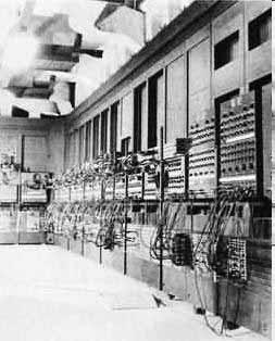
6 Transistors in Integrated Circuits 32 nm now What s the problem? Physical limit: Diffraction of light. Economical limitation: Too expensive.
.")
7 Molecular electronics: A solution The main idea: use molecules to create analogues of today s IC chips. Because molecules are small and can form structures by self-assembly. Aviram & Ratner, (1974). For example..
8 Previous measurement and modeling: Science 278, 252 (1997) 500 times of difference! PRL 84, 979 (2000)
9 As the size of a device goes down, physics change Top Channel Length, L 1 mm 0.1 mm Macroscopic dimensions < L > S. Datta, RQMP presentation (2006) Bottom 10 μm 1 μ m 0.1 μm 10 nm 1 nm 0.1 nm Atomic dimensions
10 Ohm s law:? Coherence length: Elastic mean free path: Ballistic regime:
11 Our method: How to calculate current? Landauer formula: I ( V b ) 2e h 2 T ( E, V b ) f l f r de DFT plus non-equilibrium Green s functions: Taylor, Guo, Wang, PRB 63, (2001); Waldron, Haney, Larade, MacDonald, Guo, PRL 96, (2006) Nanodcal ( & ATK


12 Conventional DFT solves two kinds of problems: Finite isolated system Gaussian-03 Periodic systems VASP Quantum transport: A device is neither finite nor periodic, and is in nonequilibrium


13 Computational modeling Interaction region Bulk region Bulk region Electronic structure Density Functional Theory (GGA) LCAO Pseudopotentials Nonequilibrium physics Full description of electrodes using ab initio self-energies Non-equilibrium electron distribution using NEGF H Calculation of electron current
14 Outline: 1. Introduction Why molecular electronics? 2. Conductance of single-molecule junctions Alkanedithiol [S-(CH 2 ) n -S] Alkanediisothiocyanate [SCN-(CH 2 )n-ncs] 3. Current-Driven Desorption at the Interface Cyclopentene on Si(100) 4. Summary
 Nano Lett.")
15 Conductance of a Au nanowire: Nature 395, 780 (1998) Nano Lett. 6, 2362 (2006)

16 Conductance of a single molecule N. J. Tao et al, Science (2003)
 1.05 N. J.")
17 Measurement on single alkanedithiol molecules R n R o exp( n) 1.05 N. J. Tao et al, JACS (2003); Science (2003)

18 Experimental results N. J. Tao et al, Faraday Discuss. 131, 145 (2006)

19 Previous modeling: Calculation Experiment N = 6 G = Unit: G 0

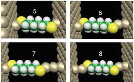
20 Our model: s s Calculation Experiment N = 6 G = N = 8 G = N = 10 G = Kaun & Seideman, Phys. Rev. B 77, (2008) Unit: G 0
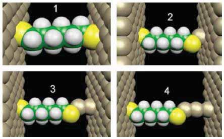
21 Contact effect (N=6): a b dxy c pz Kaun & Seideman, Phys. Rev. B 77, (2008)

22 New experimental results: N. J. Tao et al, JACS, 128, 2135 (2006)?
23 Quantitative agreement? Muller, Phys. Rev. B, 73, (2006)
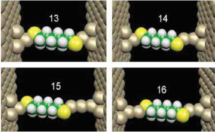
24 alkanediisothiocyanate [SCN-(CH 2 ) n -NCS] alkanedithiol [S-(CH 2 ) n -S]

25 Origin of high- and low-conductance traces in alkanediisothiocyanate single-molecule contacts Luzhbin & Kaun, Phys. Rev. B 81, (2010)
26 Luzhbin & Kaun, Phys. Rev. B 81, (2010)
27 Outline: 1. Introduction Why molecular electronics? 2. Conductance of single-molecule junctions Alkanedithiol [S-(CH 2 ) n -S] Alkanediisothiocyanate [SCN-(CH 2 )n-ncs] 3. Current-Driven Desorption at the Interface Cyclopentene on Si(100) 4. Summary
28 2. Current-Driven Desorption at the Interface: Cyclopentene on Si(100) Molecular electronic devices + silicon microelectronic technology The stability of organic molecules on semiconductors must be established.

29 Previous studies: benzene bound to Si(100) with π- orbital character Low-lying ionic resonances S. Alavi, et al., PRL 85, 5372 (2000). Saturated organic/silicon systems offer stability with respect to current-induced failure of silicon-based molecular electronics. S. N. Patitsas et al., Surf. Sci. 457, L425 (2000).
 -2V, 0.1 na N. L. Yoder et al.")
30 Desorption of cyclopentene from Si(100) Experimental results -2V, 0.1 na Elevated sample bias (threshold voltage: -2.5 and 3.5) -2V, 0.1 na N. L. Yoder et al., PRL 97, (2006); Current-Driven Phenomena in Nanoelectronics, chapter 7 (Pan Stanford, 2010)
31 Cyclopentene on Si(100): A saturated molecule Why threshold voltages is so small (-2.5 V and 3.5 V)?
32 A second question in experimental results Yield = N*e/(I*t) The yield is a factor of lower than for benzene/si(100) or chlorobenzene/si(111). A new avenue for desorption dynamics!

33 Our model: HOMO LUMO Cyclopentene Cyclopentene+Si Hybridization introduces new states into the gap N. L. Yoder et al., PRL 97, (2006); Current-Driven Phenomena in Nanoelectronics, chapter 7 (Pan Stanford, 2010)

34 PDOS peaks and the localized orbitals: The positive ion lifetime 94 fs The negative ion lifetime 257 fs

35 Geometries of cyclopentene on a Si 9 H 12 cluster: Neutral molecule Positive molecule Negative molecule
36 4. Sumary: Conductance are quantitative agree with experimental data The HC and LC may comes from the geometric configurations of electrodes Hybridization introduces new states into the gap leading to lower threshold voltages New desorption pathways are found in a cyclopentene/silicon system

37 Acknowledgements: Dr. A. Sen, Dr. D. A. Luzhbin N. L. Yoder, R. Jorn, T. Seideman and M. C. Hersam, Northwestern Univ., USA Prof. Y.-H. Tang, Dr. W. S. Su, Dr. K. Bagci, J.-H. Chen, C.-C. Su, S.-T. Pi, E. Chien, S.-T. Lin, C.-H. Hsu, Y.-C Chen, M. Lin, and Prof. C.-S. Tang.
Computational Modeling of Molecular Electronics. Chao-Cheng Kaun
 Computational Modeling of Molecular Electronics Chao-Cheng Kaun Research Center for Applied Sciences, Academia Sinica Department of Physics, National Tsing Hua University May 9, 2007 Outline: 1. Introduction
Current-Driven Phenomena in NANOELECTRONICS. Edited by Tamar Seideman Northwestern University
 Current-Driven Phenomena in NANOELECTRONICS Edited by Tamar Seideman Northwestern University Published by Pan Stanford Publishing Pte. Ltd. Penthouse Level, Suntec Tower 3 8 Temasek Boulevard Singapore
Momentum filtering effect in molecular wires
 PHYSICAL REVIEW B 70, 195309 (2004) Momentum filtering effect in molecular wires Chao-Cheng Kaun, 1, * Hong Guo, 1 Peter Grütter, 1 and R. Bruce Lennox 1,2 1 Center for the Physics of Materials and Department
Nanoelectronics. Topics
 Nanoelectronics Topics Moore s Law Inorganic nanoelectronic devices Resonant tunneling Quantum dots Single electron transistors Motivation for molecular electronics The review article Overview of Nanoelectronic
Electron transport through molecular junctions and FHI-aims
 STM m metallic surface Electron transport through molecular junctions and FHI-aims Alexei Bagrets Inst. of Nanotechnology (INT) & Steinbuch Centre for Computing (SCC) @ Karlsruhe Institute of Technology
Branislav K. Nikolić
 First-principles quantum transport modeling of thermoelectricity in nanowires and single-molecule nanojunctions Branislav K. Nikolić Department of Physics and Astronomy, University of Delaware, Newark,
Session Chair: Prof. Haiping Cheng (University of Florida) Dr. Lei Shen. National University of Singapore
 Dr. Lei Shen. National University of Singapore") B1. Modeling Quantum Transport at Nanoscale Chair(s): Chun ZHANG, National University of Singapore, Singapore Session s Title (if available) Tue - 17 Jan 2017 13:00 ~ 14:30 Room 2 Session Chair: Prof.
B1. Modeling Quantum Transport at Nanoscale Chair(s): Chun ZHANG, National University of Singapore, Singapore Session s Title (if available) Tue - 17 Jan 2017 13:00 ~ 14:30 Room 2 Session Chair: Prof.
Nanoscience, MCC026 2nd quarter, fall Quantum Transport, Lecture 1/2. Tomas Löfwander Applied Quantum Physics Lab
 Nanoscience, MCC026 2nd quarter, fall 2012 Quantum Transport, Lecture 1/2 Tomas Löfwander Applied Quantum Physics Lab Quantum Transport Nanoscience: Quantum transport: control and making of useful things
Speed-up of ATK compared to
 What s new @ Speed-up of ATK 2008.10 compared to 2008.02 System Speed-up Memory reduction Azafulleroid (molecule, 97 atoms) 1.1 15% 6x6x6 MgO (bulk, 432 atoms, Gamma point) 3.5 38% 6x6x6 MgO (k-point sampling
Title. I-V curve? e-e interactions? Conductance? Electrical Transport Through Single Molecules. Vibrations? Devices?
 Electrical Transport Through Single Molecules Harold U. Baranger, Duke University Title with Rui Liu, San-Huang Ke, and Weitao Yang Thanks to S. Getty, M. Fuhrer and L. Sita, U. Maryland Conductance? I-V
Electroluminescence from Silicon and Germanium Nanostructures
 Electroluminescence from silicon Silicon Getnet M. and Ghoshal S.K 35 ORIGINAL ARTICLE Electroluminescence from Silicon and Germanium Nanostructures Getnet Melese* and Ghoshal S. K.** Abstract Silicon
Outline. Introduction: graphene. Adsorption on graphene: - Chemisorption - Physisorption. Summary
 Outline Introduction: graphene Adsorption on graphene: - Chemisorption - Physisorption Summary 1 Electronic band structure: Electronic properties K Γ M v F = 10 6 ms -1 = c/300 massless Dirac particles!
Electron-phonon scattering from green s function transport combined with molecular dynamics: Applications to mobility predictions
 Electron-phonon scattering from green s function transport combined with molecular dynamics: Applications to mobility predictions Daniele Stradi www.quantumwise.com daniele.stradi@quantumwise.com Introduction
Electrostatics of Nanowire Transistors
 Electrostatics of Nanowire Transistors Jing Guo, Jing Wang, Eric Polizzi, Supriyo Datta and Mark Lundstrom School of Electrical and Computer Engineering Purdue University, West Lafayette, IN, 47907 ABSTRACTS
International Journal of ChemTech Research CODEN (USA): IJCRGG ISSN: Vol.7, No.2, pp ,
: IJCRGG ISSN: Vol.7, No.2, pp ,") International Journal of ChemTech Research CODEN (USA): IJCRGG ISSN: 0974-4290 Vol.7, No.2, pp 695-699, 2014-2015 ICONN 2015 [4 th -6 th Feb 2015] International Conference on Nanoscience and Nanotechnology-2015
International Journal of ChemTech Research CODEN (USA): IJCRGG ISSN: 0974-4290 Vol.7, No.2, pp 695-699, 2014-2015 ICONN 2015 [4 th -6 th Feb 2015] International Conference on Nanoscience and Nanotechnology-2015
First-Principles Modeling of the Smallest Molecular Single Electron Transistor
 Journal of Atomic, Molecular, Condensate & Nano Physics Vol. 2, No. 1, pp. 33 39, 2015 ISSN 2349-2716 (online); 2349-6088 (print) Published by RGN Publications http://www.rgnpublications.com First-Principles
Büttiker s probe in molecular electronics: Applications to charge and heat transport
 Büttiker s probe in molecular electronics: Applications to charge and heat transport Dvira Segal Department of Chemistry University of Toronto Michael Kilgour (poster) Büttiker s probe in molecular electronics:
Steady State Formalism for Electron Transfer through DNA System: Ladder Model
 Steady State Formalism for Electron Transfer through DNA System: Ladder Model S. A. Al-Seadi 1, J. M. Al-Mukh 2, S. I. Easa 2 1 Department of Physics, College of Science, ThiQar University, Nassiriya,
An ab initio approach to electrical transport in molecular devices
 INSTITUTE OF PHYSICSPUBLISHING Nanotechnology 13 (00) 1 4 An ab initio approach to electrical transport in molecular devices NANOTECHNOLOGY PII: S0957-4484(0)31500-9 JJPalacios 1,ELouis 1,AJPérez-Jiménez,ESanFabián
Investigation of Terminal Group Effect on Electron Transport Through Open Molecular Structures
 Commun. Theor. Phys. 59 (2013) 649 654 Vol. 59, No. 5, May 15, 2013 Investigation of Terminal Group Effect on Electron Transport Through Open Molecular Structures C. Preferencial Kala, 1 P. Aruna Priya,
2D Materials with Strong Spin-orbit Coupling: Topological and Electronic Transport Properties
 2D Materials with Strong Spin-orbit Coupling: Topological and Electronic Transport Properties Artem Pulkin California Institute of Technology (Caltech), Pasadena, CA 91125, US Institute of Physics, Ecole
Supporting information
 Supporting information Design, Modeling and Fabrication of CVD Grown MoS 2 Circuits with E-Mode FETs for Large-Area Electronics Lili Yu 1*, Dina El-Damak 1*, Ujwal Radhakrishna 1, Xi Ling 1, Ahmad Zubair
Computational electronics from atomic principles - basics of electronic transport. Hong Guo
 Computational electronics from atomic principles - basics of electronic transport Hong Guo Center for the Physics of Materials and Dept. of Physics, McGill Univ., Montreal, Canada Introduction: need for
are microscopically large but macroscopically small contacts which may be connected to a battery to provide the bias voltage across the junction.
 At present, we observe a long-lasting process of miniaturization of electronic devices. The ultimate limit for the miniaturization of electronic components is set by the atomic scale. However, in the case
First-principles nonequilibrium analysis of STMinduced molecular negative-differential resistance on Si(100)
") Purdue University Purdue e-pubs Birck and NCN Publications Birck Nanotechnology Center July 2008 First-principles nonequilibrium analysis of STMinduced molecular negative-differential resistance on Si(100)
Purdue University Purdue e-pubs Birck and NCN Publications Birck Nanotechnology Center July 2008 First-principles nonequilibrium analysis of STMinduced molecular negative-differential resistance on Si(100)
Organic Electronic Devices
 Organic Electronic Devices Week 5: Organic Light-Emitting Devices and Emerging Technologies Lecture 5.5: Course Review and Summary Bryan W. Boudouris Chemical Engineering Purdue University 1 Understanding
Introduction to Nanotechnology Chapter 5 Carbon Nanostructures Lecture 1
 Introduction to Nanotechnology Chapter 5 Carbon Nanostructures Lecture 1 ChiiDong Chen Institute of Physics, Academia Sinica chiidong@phys.sinica.edu.tw 02 27896766 Carbon contains 6 electrons: (1s) 2,
Electrical conductivity of metal carbon nanotube structures: Effect of length and doping
 Bull. Mater. Sci., Vol. 37, No. 5, August 2014, pp. 1047 1051. Indian Academy of Sciences. Electrical conductivity of metal carbon nanotube structures: Effect of length and doping R NIGAM 1, *, S HABEEB
Direct Measurement of Electron Transfer through a Hydrogen Bond
 Supporting Information Direct Measurement of Electron Transfer through a Hydrogen Bond between Single Molecules Tomoaki Nishino,*, Nobuhiko Hayashi, and Phuc T. Bui Nanoscience and Nanotechnology Research
ᣂቇⴚ㗔 䇸䉮䊮䊏䊠䊷䊁䉞䉪䉴䈮䉋䉎 䊂䉱䉟䊮䋺ⶄว 㑐䈫㕖ᐔⴧ䉻䉟䊅䊚䉪䉴䇹 ᐔᚑ22ᐕᐲ ળ䇮2011ᐕ3 4ᣣ䇮 ੩ᄢቇᧄㇹ䉨䊞䊮䊌䉴 㗄 A02 ኒᐲ 㑐ᢙᴺℂ 䈮ၮ䈨䈒㕖ᐔⴧ 䊅䊉䉴䉬䊷䊦㔚 વዉ䉻䉟䊅䊚䉪䉴 ઍ ᄢᎿ ㆺ
 22201134 A02 GCOE Si device (further downsizing) Novel nanostructures (such as atomic chain) Nanoscale multi-terminal resistance measurement Carbon nanotube transistor Atomic switch Interplay:l Dynamics:
Support information: (a) + + (b)
 + + (b)") 1 upport information: Mechanism of the toddart-heath bistable rotaxane molecular switch Abstract The supporting information is organized as follows: ection 1 describes the real device and our strategy
1 upport information: Mechanism of the toddart-heath bistable rotaxane molecular switch Abstract The supporting information is organized as follows: ection 1 describes the real device and our strategy
CITY UNIVERSITY OF HONG KONG. Theoretical Study of Electronic and Electrical Properties of Silicon Nanowires
 CITY UNIVERSITY OF HONG KONG Ë Theoretical Study of Electronic and Electrical Properties of Silicon Nanowires u Ä öä ªqk u{ Submitted to Department of Physics and Materials Science gkö y in Partial Fulfillment
Microscopy and Spectroscopy with Tunneling Electrons STM. Sfb Kolloquium 23rd October 2007
 Microscopy and Spectroscopy with Tunneling Electrons STM Sfb Kolloquium 23rd October 2007 The Tunnel effect T ( E) exp( S Φ E ) Barrier width s Barrier heigth Development: The Inventors 1981 Development:
GW-like approaches to quantum transport. Rex Godby
 GW-like approaches to quantum transport Rex Godby Outline Introduction to the quantum transport problem Ab initio quantum conductance in the presence of e e interaction (TDDFT / MBPT) 2 + Bothersome aspects
Band calculations: Theory and Applications
 Band calculations: Theory and Applications Lecture 2: Different approximations for the exchange-correlation correlation functional in DFT Local density approximation () Generalized gradient approximation
arxiv: v1 [cond-mat.mes-hall] 3 Apr 2014
![arxiv: v1 [cond-mat.mes-hall] 3 Apr 2014](/thumbs/87/96174140.jpg "arxiv: v1 [cond-mat.mes-hall] 3 Apr 2014") Gate Controlled Molecular Switch Based on picene-f4 TCNQ Charge-Transfer Material Torsten Hahn, Simon Liebing, and Jens Kortus We show that the recently synthesized charge-transfer material picene-f4 TCNQ
Gate Controlled Molecular Switch Based on picene-f4 TCNQ Charge-Transfer Material Torsten Hahn, Simon Liebing, and Jens Kortus We show that the recently synthesized charge-transfer material picene-f4 TCNQ
Quantum Transport: electron-electron and electron-phonon effects. Rex Godby
 Quantum Transport: electron-electron and electron-phonon effects Rex Godby Outline Introduction to the quantum transport problem Ab initio quantum conductance in the presence of e-e interaction (TDDFT
Supporting Information. Charge Transport Across Insulating. Self-Assembled Monolayers: Non-Equilibrium. Approaches and Modeling to Relate Current and
 Supporting Information Charge Transport Across Insulating Self-Assembled Monolayers: Non-Equilibrium Approaches and Modeling to Relate Current and Molecular Structure Fatemeh Mirjani,, Joseph M. Thijssen,
Impact of Silicon Wafer Orientation on the Performance of Metal Source/Drain MOSFET in Nanoscale Regime: a Numerical Study
 JNS 2 (2013) 477-483 Impact of Silicon Wafer Orientation on the Performance of Metal Source/Drain MOSFET in Nanoscale Regime: a Numerical Study Z. Ahangari *a, M. Fathipour b a Department of Electrical
Lecture 04 Review of MOSFET
 ECE 541/ME 541 Microelectronic Fabrication Techniques Lecture 04 Review of MOSFET Zheng Yang (ERF 3017, email: yangzhen@uic.edu) What is a Transistor? A Switch! An MOS Transistor V GS V T V GS S Ron D
Electronic structure and transport in silicon nanostructures with non-ideal bonding environments
 Purdue University Purdue e-pubs Other Nanotechnology Publications Birck Nanotechnology Center 9-15-2008 Electronic structure and transport in silicon nanostructures with non-ideal bonding environments
Lecture 12. Electron Transport in Molecular Wires Possible Mechanisms
 Lecture 12. Electron Transport in Molecular Wires Possible Mechanisms In Lecture 11, we have discussed energy diagrams of one-dimensional molecular wires. Here we will focus on electron transport mechanisms
The Critical Role of Quantum Capacitance in Compact Modeling of Nano-Scaled and Nanoelectronic Devices
 The Critical Role of Quantum Capacitance in Compact Modeling of Nano-Scaled and Nanoelectronic Devices Zhiping Yu and Jinyu Zhang Institute of Microelectronics Tsinghua University, Beijing, China yuzhip@tsinghua.edu.cn
Spectroscopy of nanostructures: from optics to transport
 Spectroscopy of nanostructures: from optics to transport Angel Rubio NanoBio Spectroscopy Group, Dpto. Física de Materiales, Universidad del País Vasco, Centro Mixto CSIC UPV/EHU and DIPC Edificio Korta,
Spring Semester 2012 Final Exam
 Spring Semester 2012 Final Exam Note: Show your work, underline results, and always show units. Official exam time: 2.0 hours; an extension of at least 1.0 hour will be granted to anyone. Materials parameters
PHYSICAL REVIEW B 70, (2004) (Received 23 November 2003; revised manuscript received 16 March 2004; published 24 August 2004)
 (Received 23 November 2003; revised manuscript received 16 March 2004; published 24 August 2004)") PHYSICAL REVIEW B 70, 085410 (2004) Electron transport through molecules: Self-consistent and non-self-consistent approaches San-Huang Ke, 1,2 Harold U. Baranger, 2 and Weitao Yang 1 1 Department of Chemistry,
PHYSICAL REVIEW B 70, 085410 (2004) Electron transport through molecules: Self-consistent and non-self-consistent approaches San-Huang Ke, 1,2 Harold U. Baranger, 2 and Weitao Yang 1 1 Department of Chemistry,
Introduction to Molecular Electronics. Lecture 1: Basic concepts
 Introduction to Molecular Electronics Lecture 1: Basic concepts Conductive organic molecules Plastic can indeed, under certain circumstances, be made to behave very like a metal - a discovery for which
From exhaustive simulations to key principles in DNA nanoelectronics
 From exhaustive simulations to key principles in DNA nanoelectronics Dvira Segal Department of Chemistry University of Toronto Roman Korol (undergrad) Hyehwang Kim (undergrad) Michael Kilgour (grad) Challenge:
Wafer-scale fabrication of graphene
 Wafer-scale fabrication of graphene Sten Vollebregt, MSc Delft University of Technology, Delft Institute of Mircosystems and Nanotechnology Delft University of Technology Challenge the future Delft University
(Co-PIs-Mark Brongersma, Yi Cui, Shanhui Fan) Stanford University. GCEP Research Symposium 2013 Stanford, CA October 9, 2013
 Stanford University. GCEP Research Symposium 2013 Stanford, CA October 9, 2013") High-efficiency thin film nano-structured multi-junction solar James S. cells Harris (PI) (Co-PIs-Mark Brongersma, Yi Cui, Shanhui Fan) Stanford University GCEP Research Symposium 2013 Stanford, CA October
High-efficiency thin film nano-structured multi-junction solar James S. cells Harris (PI) (Co-PIs-Mark Brongersma, Yi Cui, Shanhui Fan) Stanford University GCEP Research Symposium 2013 Stanford, CA October
First-Principle Studies on Adsorption of Cu + and Hydrated Cu + Cations on Clean Si(111) Surface
 Surface") CHEM. RES. CHINESE UNIVERSITIES 2010, 26(3), 472 478 First-Principle Studies on Adsorption of Cu + and Hydrated Cu + Cations on Clean Si(111) Surface CHENG Feng-ming 1,2, SHENG Yong-li 1,3, LI Meng-hua
CHEM. RES. CHINESE UNIVERSITIES 2010, 26(3), 472 478 First-Principle Studies on Adsorption of Cu + and Hydrated Cu + Cations on Clean Si(111) Surface CHENG Feng-ming 1,2, SHENG Yong-li 1,3, LI Meng-hua
Identifying the rate-limiting processes at the Li-air cathode
 Identifying the rate-limiting processes at the Li-air cathode Tejs Vegge Risø DTU, National Laboratory for Sustainable Energy and Center for Atomic-scale Materials Design, Technical University of Denmark
Molecular electronics. Lecture 2
 Molecular electronics Lecture 2 Molecular electronics approach Electrodes and contacts Basic requirement for molecular electronics: connection of the molecule of interest to the outside world, i.e. electrode
Transport through Andreev Bound States in a Superconductor-Quantum Dot-Graphene System
 Transport through Andreev Bound States in a Superconductor-Quantum Dot-Graphene System Nadya Mason Travis Dirk, Yung-Fu Chen, Cesar Chialvo Taylor Hughes, Siddhartha Lal, Bruno Uchoa Paul Goldbart University
Chapter 4: Bonding in Solids and Electronic Properties. Free electron theory
 Chapter 4: Bonding in Solids and Electronic Properties Free electron theory Consider free electrons in a metal an electron gas. regards a metal as a box in which electrons are free to move. assumes nuclei
Role of Surface Chemistry on Charge Carrier Transport in Quantum Dot Solids
 Role of Surface Chemistry on Charge Carrier Transport in Quantum Dot Solids Cherie R. Kagan, University of Pennsylvania in collaboration with the Murray group Density of Electronic States in Quantum Dot
Charge relaxation resistance at atomic scale: An ab initio calculation
 Title Charge relaxation resistance at atomic scale: An ab initio calculation Author(s) Wang, B; Wang, J Citation Physical Review B (Condensed Matter and Materials Physics), 2008, v. 77, article no. 245309
Carbon Nanotubes in Interconnect Applications
 Carbon Nanotubes in Interconnect Applications Page 1 What are Carbon Nanotubes? What are they good for? Why are we interested in them? - Interconnects of the future? Comparison of electrical properties
single-electron electron tunneling (SET)
") single-electron electron tunneling (SET) classical dots (SET islands): level spacing is NOT important; only the charging energy (=classical effect, many electrons on the island) quantum dots: : level spacing
single-electron electron tunneling (SET) classical dots (SET islands): level spacing is NOT important; only the charging energy (=classical effect, many electrons on the island) quantum dots: : level spacing
New Volleyballenes: Y 20 C 60, La 20 C 60, and Lu 20 C 60
 New Volleyballenes: Y 20 C 60, La 20 C 60, and Lu 20 C 60 Jing Wang a and Ying Liu*,a,b a Department of Physics and Hebei Advanced Thin Film Laboratory, Hebei Normal University, Shijiazhuang 050016, Hebei,
DFT EXERCISES. FELIPE CERVANTES SODI January 2006
 DFT EXERCISES FELIPE CERVANTES SODI January 2006 http://www.csanyi.net/wiki/space/dftexercises Dr. Gábor Csányi 1 Hydrogen atom Place a single H atom in the middle of a largish unit cell (start with a
Search for materials to harvest light
 Solar nanocomposites with complementary charge extraction pathways for electrons and holes: Si embedded in ZnS S. Wippermann, M. Vörös, F. Gygi, A. Gali, G. Zimanyi, G. Galli NanoMatFutur DPG-2014, 04/03/2014
Canadian Journal of Chemistry. Spin-dependent electron transport through a Mnphthalocyanine. Draft
 Spin-dependent electron transport through a Mnphthalocyanine molecule: an SS-DFT study Journal: Manuscript ID cjc-216-28 Manuscript Type: Article Date Submitted by the Author: 6-Jun-216 Complete List of
Lecture 28 - The Long Metal-Oxide-Semiconductor Field-Effect Transistor (cont.) April 18, 2007
 April 18, 2007") 6.720J/3.43J - Integrated Microelectronic Devices - Spring 2007 Lecture 28-1 Lecture 28 - The Long Metal-Oxide-Semiconductor Field-Effect Transistor (cont.) April 18, 2007 Contents: 1. Second-order and
6.720J/3.43J - Integrated Microelectronic Devices - Spring 2007 Lecture 28-1 Lecture 28 - The Long Metal-Oxide-Semiconductor Field-Effect Transistor (cont.) April 18, 2007 Contents: 1. Second-order and
Electronic Supporting Information for
 Electronic Supplementary Material (ESI) for Materials Horizons. This journal is The Royal Society of Chemistry 2015 Electronic Supporting Information for Probing the Energy Levels in Hole-doped Molecular
3-month progress Report
 3-month progress Report Graphene Devices and Circuits Supervisor Dr. P.A Childs Table of Content Abstract... 1 1. Introduction... 1 1.1 Graphene gold rush... 1 1.2 Properties of graphene... 3 1.3 Semiconductor
Goal: To use DNA self-assembly to overcome the challenges of optical and e-beam lithography in creating nanoscale circuits.
 Goal: To use DNA self-assembly to overcome the challenges of optical and e-beam lithography in creating nanoscale circuits. PI Paul Rothemund, computer scientist, Senior Research Associate (research faculty)
Tunable Band Gap of Silicene on Monolayer Gallium Phosphide Substrate
 2017 International Conference on Energy Development and Environmental Protection (EDEP 2017) ISBN: 978-1-60595-482-0 Tunable Band Gap of Silicene on Monolayer Gallium Phosphide Substrate Miao-Juan REN
Electronic structure mechanism of spin-polarized electron transport in a Ni C 60 Ni system
 Chemical Physics Letters 439 (27) 11 114 www.elsevier.com/locate/cplett Electronic structure mechanism of spin-polarized electron transport in a Ni C 6 Ni system Haiying He a, Ravindra Pandey a, *, Shashi
Coulomb blockade and single electron tunnelling
 Coulomb blockade and single electron tunnelling Andrea Donarini Institute of theoretical physics, University of Regensburg Three terminal device Source System Drain Gate Variation of the electrostatic
EE650R: Reliability Physics of Nanoelectronic Devices Lecture 18: A Broad Introduction to Dielectric Breakdown Date:
 EE650R: Reliability Physics of Nanoelectronic Devices Lecture 18: A Broad Introduction to Dielectric Breakdown Date: Nov 1, 2006 ClassNotes: Jing Li Review: Sayeef Salahuddin 18.1 Review As discussed before,
Extrinsic Origin of Persistent Photoconductivity in
 Supporting Information Extrinsic Origin of Persistent Photoconductivity in Monolayer MoS2 Field Effect Transistors Yueh-Chun Wu 1, Cheng-Hua Liu 1,2, Shao-Yu Chen 1, Fu-Yu Shih 1,2, Po-Hsun Ho 3, Chun-Wei
Charge fluctuators, their temperature and their response to sudden electrical fields
 Charge fluctuators, their temperature and their response to sudden electrical fields Outline Charge two-level fluctuators Measuing noise with an SET Temperature and bias dependence of the noise TLF temperature
Quantum Transport Beyond the Independent-Electron Approximation. Rex Godby
 Quantum Transport Beyond the Independent-Electron Approximation Rex Godby Outline Introduction to the quantum transport problem Ab initio quantum conductance in the presence of e e interaction (TDDFT /
Fig. 8.1 : Schematic for single electron tunneling arrangement. For large system this charge is usually washed out by the thermal noise
 Part 2 : Nanostuctures Lecture 1 : Coulomb blockade and single electron tunneling Module 8 : Coulomb blockade and single electron tunneling Coulomb blockade and single electron tunneling A typical semiconductor
 www.iue.tuwien.ac.at/wigner-wiki/ quantum r rmnh h h E a n = a E b n = b h h h n = 1 n = 1 n = 1 0.53 h h n h cos sin 1 1 N ψ = 1 N! ϕ n1 (x 1 ) ϕ n2 (x 1 ) ϕ nn (x 1 ) ϕ n1 (x 2 ) ϕ n2 (x 2
Saroj P. Dash. Chalmers University of Technology. Göteborg, Sweden. Microtechnology and Nanoscience-MC2
 Silicon Spintronics Saroj P. Dash Chalmers University of Technology Microtechnology and Nanoscience-MC2 Göteborg, Sweden Acknowledgement Nth Netherlands University of Technology Sweden Mr. A. Dankert Dr.
Olivier Bourgeois Institut Néel
 Olivier Bourgeois Institut Néel Outline Introduction: necessary concepts: phonons in low dimension, characteristic length Part 1: Transport and heat storage via phonons Specific heat and kinetic equation
Quantum Transport in Ultracold Atoms. Chih-Chun Chien ( 簡志鈞 ) University of California, Merced
 University of California, Merced") Quantum Transport in Ultracold Atoms Chih-Chun Chien ( 簡志鈞 ) University of California, Merced Outline Introduction to cold atoms Atomtronics simulating and complementing electronic devices using cold atoms
Quantum Transport in Ultracold Atoms Chih-Chun Chien ( 簡志鈞 ) University of California, Merced Outline Introduction to cold atoms Atomtronics simulating and complementing electronic devices using cold atoms
RSC Advances.
 This is an Accepted Manuscript, which has been through the Royal Society of Chemistry peer review process and has been accepted for publication. Accepted Manuscripts are published online shortly after
How a single defect can affect silicon nano-devices. Ted Thorbeck
 How a single defect can affect silicon nano-devices Ted Thorbeck tedt@nist.gov The Big Idea As MOS-FETs continue to shrink, single atomic scale defects are beginning to affect device performance Gate Source
Electro-Thermal Transport in Silicon and Carbon Nanotube Devices E. Pop, D. Mann, J. Rowlette, K. Goodson and H. Dai
 Electro-Thermal Transport in Silicon and Carbon Nanotube Devices E. Pop, D. Mann, J. Rowlette, K. Goodson and H. Dai E. Pop, 1,2 D. Mann, 1 J. Rowlette, 2 K. Goodson 2 and H. Dai 1 Dept. of 1 Chemistry
Modeling Transport in Heusler-based Spin Devices
 Modeling Transport in Heusler-based Spin Devices Gautam Shine (Stanford) S. Manipatruni, A. Chaudhry, D. E. Nikonov, I. A. Young (Intel) Electronic Structure Extended Hückel theory Application to Heusler
2. TranSIESTA 1. SIESTA. DFT In a Nutshell. Introduction to SIESTA. Boundary Conditions: Open systems. Greens functions and charge density
 1. SIESTA DFT In a Nutshell Introduction to SIESTA Atomic Orbitals Capabilities Resources 2. TranSIESTA Transport in the Nanoscale - motivation Boundary Conditions: Open systems Greens functions and charge
Dmitry Ryndyk. December 20, 2007, Dresden. In collaboration with Pino D Amico, Klaus Richter, and Gianaurelio Cuniberti
 Memory effect in electron-vibron systems Dmitry Ryndyk December 20, 2007, Dresden In collaboration with Pino D Amico, Klaus Richter, and Gianaurelio Cuniberti Complex Quantum Systems Institute for Theoretical
JFETs - MESFETs - MODFETs
 Technische Universität raz Institute of Solid State Physics JFETs - MESFETs - MOFETs JFET n n-channel JFET S n-channel JFET x n 2 ( Vbi V) en S p-channel JFET 2 Pinch-off at h = x en n h Vp 2 V p = pinch-off
Designing Principles of Molecular Quantum. Interference Effect Transistors
 Suorting Information for: Designing Princiles of Molecular Quantum Interference Effect Transistors Shuguang Chen, GuanHua Chen *, and Mark A. Ratner * Deartment of Chemistry, The University of Hong Kong,
Sfb 658 Colloquium 11 May Part II. Introduction to Two-Photon-Photoemission (2PPE) Spectroscopy. Martin Wolf
 Spectroscopy. Martin Wolf") Sfb 658 Colloquium 11 May 2006 Part II Introduction to Two-Photon-Photoemission (2PPE) Spectroscopy Martin Wolf Motivation: Electron transfer across interfaces key step for interfacial and surface dynamics
Sfb 658 Colloquium 11 May 2006 Part II Introduction to Two-Photon-Photoemission (2PPE) Spectroscopy Martin Wolf Motivation: Electron transfer across interfaces key step for interfacial and surface dynamics
Applications of Gaussian Process Model in Molecular Dynamics University of British Columbia Vancouver, Canada. Roman Krems
 Applications of Gaussian Process Model in Molecular Dynamics University of British Columbia Vancouver, Canada Roman Krems Gaussian Process Model for Collision Dynamics of Complex Molecules, Jie Cui and
Molecular Electronics
 Molecular Electronics An Introduction to Theory and Experiment Juan Carlos Cuevas Universidad Autönoma de Madrid, Spain Elke Scheer Universität Konstanz, Germany 1>World Scientific NEW JERSEY LONDON SINGAPORE
Measurement of Current-Induced Local Heating in a Single Molecule Junction
 Measurement of Current-Induced Local Heating in a Single Molecule Junction NANO LETTERS 2006 Vol. 6, No. 6 1240-1244 Zhifeng Huang, Bingqian Xu, Yuchang Chen, Massimiliano Di Ventra,*, and Nongjian Tao*,
High Quality Thin Graphene Films from Fast. Research Center for Applied Sciences, Academia Sinica, Taipei, 11529, Taiwan
 Supporting Materials High Quality Thin Graphene Films from Fast Electrochemical Exfoliation Ching-Yuan Su, Ang-Yu Lu #, Yanping Xu, Fu-Rong Chen #, Andrei N. Khlobystov $ and Lain-Jong Li * Research Center
Drift-diffusion model for single layer transition metal dichalcogenide field-effect transistors
 Drift-diffusion model for single layer transition metal dichalcogenide field-effect transistors David Jiménez Departament d'enginyeria Electrònica, Escola d'enginyeria, Universitat Autònoma de Barcelona,
Evaluation of Electronic Characteristics of Double Gate Graphene Nanoribbon Field Effect Transistor for Wide Range of Temperatures
 Evaluation of Electronic Characteristics of Double Gate Graphene Nanoribbon Field Effect Transistor for Wide Range of Temperatures 1 Milad Abtin, 2 Ali Naderi 1 Department of electrical engineering, Masjed
wire z axis Under these assumptions, if we model the electrons by plane waves in the z direction we get n E, n, 1,2,
 Part 4. Two Terminal Quantum Wire Devices Part 4. Two Terminal Quantum Wire Devices Let s consider a quantum wire between two contacts. As we saw in Part, a quantum wire is a one-dimensional conductor.
 Image courtesy of Keith Schwab http://www.lbl.gov/science-articles/archive/afrd Articles/Archive/AFRD-quantum-logic.html http://www.wmi.badw.de/sfb631/tps/dqd2.gif http://qist.lanl.gov/qcomp_map.shtml
Nanomaterials for Plasmonic Devices. Lih J. Chen
 Nanomaterials for Plasmonic Devices Lih J. Chen Department of Materials Science and Engineering, National Tsing Hua University, Hsinchu, Taiwan Papers on Plasmon: 75,000 (6/25/2018) Papers on Plasmonics:
Planar Organic Photovoltaic Device. Saiful I. Khondaker
 Planar Organic Photovoltaic Device Saiful I. Khondaker Nanoscience Technology Center and Department of Physics University of Central Florida http://www.physics.ucf.edu/~khondaker W Metal 1 L ch Metal 2
Electron Transport in Molecular Wire Junctions. Abraham Nitzan 1 and Mark A. Ratner 2
 REVIEW Electron Transport in Molecular Wire Junctions Abraham Nitzan 1 and Mark A. Ratner 2 Molecular conductance junctions are structures in which single molecules or small groups of molecules conduct
Kinetic equation approach to the problem of rectification in asymmetric molecular structures
 Kinetic equation approach to the problem of rectification in asymmetric molecular structures Kamil Walczak Institute of Physics, Adam Mickiewicz University Umultowska 85, 6-64 Poznań, Poland Transport