Mesoscopic superlattices
|
|
|
- Ann Anderson
- 6 years ago
- Views:
Transcription
1 Mesoscopic superlattices

2 Mesoscopic superlattices Periodic arrays of mesoscopic elements. Lateral superlattices can be imposed onto a 2DEG by lithographic techniques. One-dimensional superlattices Patterned by holographic methods interference of laser beams, a > 200 nm. Shorter scales can be done using electron bean or scanning probe lithography, but accuracy is lower. The photo-resist is illuminated by the periodically modulated interference pattern of two laser beams. 1. Give examples of mesoscopic superlattices. Describe methods of their preparation. What could be dimension and spatial resolution of practically useful superlattices? What new physics and unusual features would one expect in superlattices? Superlattices 2

3 The resist can be used as Preparation a mask for lift-off process; for modulation of distance between the gate and 2DEG; as an etch mask Interesting manifestation Weiss oscillations, similar to Shubnikov-de Haas and also periodic in 1/B. They occur in weak magnetic fields and are anisotropic. Superlattices 3

4 Sh-dH Weiss oscillations The density modulation is only 2%, but the effect is very large! Why? The reason is the drift of the cyclotron orbits induces by periodic electric field of the superlattice. The local drift is proportional to ExB. Let us assume r c >> a. Then for most parts of the trajectory the drift averages to zero. The drift in x-direction is mostly accumulated near the turning points, and it is important that its signs are the same or opposite. 2. Describe Weiss oscillations. What is their periodicity in magnetic field? In what kind of superlattices do they take place? Are they anisotropic? Superlattices 4

5 Weiss oscillations If this drift has the same sign for the electron motion in the positive and negative x-direction, a net drift will remain for a complete cyclotron motion. The result from the calculation in the limit of r c >> a reads: It emerges from approximating the Bessel function It predicts that the oscillations are periodic in 1/B, that the oscillation amplitude increases as B is increased, and that the oscillations vanish for r c < a, in good agreement with the experiment. This result holds only for r c >> a, however. The theory assumes a sinusoidal superlattice potential. Other potential shapes will give phases that differ from π/4. 3. How can small electron density modulation lead to strong Weiss oscillations? Give semiclassical description of the oscillations by introducing cyclotron orbits and analysing local drift of electrons. Superlattices 5
6 Two-dimensional superlattices One can use the above procedure twice, second time after rotating by 90 o. The so-called antidot lattices are just 2D systems of holes in 2DEG. One can find the discrete values of magnetic field at which the orbits do not hit the scatterers so-called commensurate fields. For a square lattice they enclose 1,2,4,9,21, antidots 4. Give example of a two-dimensional superlattice. What are antidot lattices and their commensurate fields? How can commensurate fields result in increased resistivity? Superlattices 6
7 Classical and quantum mechanics of 2DEG Classical motion: Lorentz force: Perpendicular to the velocity! Newtonian equation of motion: m*v 2 /r c = evb; v=ebr c /m*; =v/2 r c ; c =2 =eb/m* Cyclotron orbit Cyclotron frequency, Cyclotron radius, In classical mechanics, any size of the orbit is allowed. Magnetotransport in 2DEG
 20000 40000 1/B (1/T) Superlattice is reflected in oscillations of magnetic moment of superconducting film.")
8 m (emu) P (arb. u.) Antidots superlattice in YBa 2 Cu 3 O 7 film B = 0.3 Oe T=72 K E K 88.5 K 89 K 0.00E B (T) /B (1/T) Superlattice is reflected in oscillations of magnetic moment of superconducting film. Superlattices 8


9 Antidots superlattice in YBa 2 Cu 3 O 7 film : MOI Optical MOI Superlattice guide magnetic flux motion in superconducting film. Planar sample size is 5 mm. Superlattices 9

10 2D self-assembly of nanoparticles Three-dimensional AFM image of Au nanoparticles on STO substrate deposited with 25 laser pulses at 780 C. The height of the pixels is scaled with the planar sizes in the plot.

11 Columnar structure of YBCO on 2D array of nanoparticles TEM image of a cross-sectional area inside YBCO film grown on substrate decorated with Ag nano-particles. A regular nanometerscale columnar structure is seen in the image.
12 Semiconducting sensor device: structure
13 Semiconducting sensor device: structure


14 Shape-sensitive crystallization in colloidal superball fluids, Laura Rossia et al., PNAS April 28, 2015 vol. 112 no. 17 Since antiquity it has been known that particle shape plays an essential role in the symmetry and structure of matter. A familiar example comes from dense packings, such as spheres arranged in a face-centered cubic lattice. For colloidal superballs, we observe the transition from hexagonal to rhombic crystals consistent with the densest packings. In addition, we see the existence of square structures promoted by the presence of depletion attractions in the colloidal system. (Scale bars: 1 μm.) SEM images of the silica superballs used for the experiments. Introduction 14

15 Electrostatic assembly of binary nanoparticle superlattices using protein cages, Mauri A. Kostiainen et al., NATURE NANOTECHNOLOGY VOL 8 JANUARY Protein-based nanocages provide a complex yet monodisperse and geometrically welldefined hollow cage that can be used to encapsulate different materials. Such protein cages have been used to program the self-assembly of encapsulated materials to form free-standing crystals and superlattices at interfaces or in solution. Here, we show that electrostatically patchy protein cages cowpea chlorotic mottle virus and ferritin cages can be used to direct the self-assembly of three-dimensional binary superlattices. Scale bar, 50 nm Introduction 15


16 Two-dimensional superlattices One can use the above procedure twice, second time after rotating by 90 o. The so-called antidot lattices are just 2D systems of holes in 2DEG. One can find the discrete values of magnetic field at which the orbits do not hit the scatterers so-called commensurate fields. For a square lattice they enclose 1,2,4,9,21, antidots 4. Give example of a two-dimensional superlattice. What are antidot lattices and their commensurate fields? How can commensurate fields result in increased resistivity? Superlattices 16
17 Low field resistivity peaks These values correspond to increased resistivity. However: Resistivity maxima are not exactly at the expected positions; An unexpected negative Hall resistance has been observed How these features can be explained? Superlattices 17
18 Hall effect Consider results of modeling for a simple layout for measuring the Hall effect. An example is the antidot lattice with lattice constants a = 240 nm and b = 480 nm. The potential can be modeled as In the model, it is assumed = 2, while V 0 and β are chosen such that the antidot potential peaks out of the Fermi sea with a radius of 43 nm. 5. Introduce an approach to analyse Hall Effect and longitudinal resistance in antidot superlattices. What is realistic potential for electrons in isotropic and anisotropic antidot lattices and how it affects the resistance? Superlattices 18

19 Poincaré sections For square lattice: In the absence of electric fields the phase space consists of two separate regions, called the chaotic and regular regions. Electric field does not destroy pinning. 6. Describe technique of Poincaré sections. How can they shade light on the evolution of electron motion? Does bias voltage mix the chaotic and regular regions of the phase space? Is it correct that electrons in the regular regions are main carriers of current? Superlattices 19
20 Effect of driving electric field When a weak electric field applied, the electrons that started out inside a regular region remain therein, while all other electrons have escaped the monitored region (in the y-direction). This numerical result indicates that even a bias voltage does not mix the chaotic and regular regions of the phase space. Superlattices 20
21 Origin of conduction (a) Fraction of the phase space volume of the regular regions of the phase space for a square antidot lattice, (b) the longitudinal resistance of the chaotic electrons, and (c) the calculated resistance (full line) as compared with the measured one. The electrons in the regular regions cannot carry current, which is rather carried by electrons with chaotic dynamics. Therefore, the conductance is obtained from the contribution of the chaotic electrons Superlattices 21
22 Simulated trajectories The trajectories for r c = a/2 Arrows typical trajectories Insets positions of 1000 electrons after 135 ps in the area of 24x24 lattice periods Superlattices 22
23 Magnetic field dependency of conductance Main features: Peaks in σ xx and smooth σ yy is observed field increases; decrease of as magnetic At magnetic fields indicated by A and C the conductivity is approximately isotropic, while at the fields B and D they differ by a factor 25. These features can be understood from the shapes of typical trajectories. Superlattices 23

24 Conductivity tensor Magnetic field is applied in the z-direction, B = (0, 0, B) Important quantity is the product of the cyclotron frequency, by the relaxation time, S is a geometry factor Here v i are the components of the drift velocity vector. Solving this system of equations for j gives j = ^ σe with conductivity as a tensor, Resistivity tensor, Update of solid state physics 24
25 Electron trajectories At large magnetic field the electrons are trapped by antidots and conductance is very low. It is still easier to diffuse along x since a < b. At σ xx -peaks antidots channel electron along x-direction There is no preferred directions of diffusion Similar trends are seen from the picture of diffusing electron clouds (insets) Superlattices 25

26 Conductance description One can model diffusion instead of conductance using the Einstein relation. On the other hand, the current must be proportional to the gradient of the electrochemical potential, Thus Now, how one can model diffusion? 7. Can description of conductance be given using a diffusion model? Is Kubo formula applicable in this case? Can you comment on classical and quantum Kubo formulae? What is the diffusion coefficient in the Kubo formula in an absence of magnetic field and driving force? Superlattices 26


27 Brownian motion An explanation of electrons behaviour is in the theory of Brownian motion, see courses in statistical physics. In this theory a particle is assumed to be subjected to random forces, which make velocity a random quantity. Then: classical Kubo formula Here: Superlattices 27

28 Kubo formula The expression on previous slide is sometimes called the classical Kubo formula. According to quantum mechanics, velocities are operators which do not commute at different times. Then calculation is much more difficult. In the absence of magnetic field and driving force, Thus where d is the dimensionality of the system Superlattices 28
29 Quantum effects In hexagonal antidot lattices, additional oscillations can be observed, which are periodic in B. It is the result of enhanced backscattering due to phase coherent Altshuler Aronov Spivak (AAS) oscillations (a) Longitudinal magneto-resistivities in square and hexagonal antidot lattices (the lattice geometries are shown in the inset). (b) Enlargement of xx for the hexagonal lattice around B = 0, which oscillates with a period of B = h/2e A, where A is the average area of one antidot. The strong temperature dependence indicates a phase coherent origin. 8. Can quantum effects be seen in the behaviour of superlattices in strong magnetic field? Does anything unusual happen in hexagonal antidot lattice? If yes, can you give possible quantum interpretation of the effect? Superlattices 29


30 Bohr-Sommerfeld quantization rule The number of wavelength along the trajectory must be integer. Only discrete values of the trajectory radius are allowed Energy spectrum: ω c τ 1 Landau levels Wave functions are smeared around classical orbits with r n = l B (n+1) 1/2 ; l B = (ħ/ c m) 1/2 l B is called the magnetic length. It is radius of classical electron orbit for n = 0. v/r; r v/ ; mv 2 /2= ħ c (n+1/2); v n 0 = (ħ c /m) 1/2 ; l B = r n 0 = (ħ/ c m) 1/2 Magnetotransport in 2DEG
31 Density of states Two dimensional system, periodic boundary conditions Momentum is quantized in units of A quadratic lattice in k-space, each of them is g-fold degenerate (spin, valleys). Assume that, the limit of continuous spectrum. Number of states between k and k+dk: Update of solid state physics 31


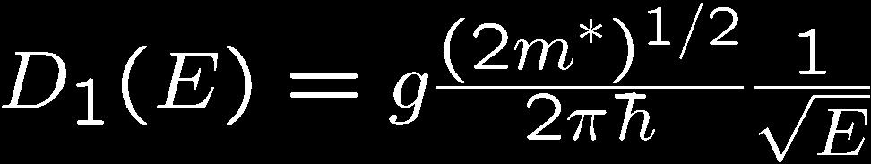
32 Density of states in 2D Number of states per volume per the region k,k+dk Density of states -Number of states per volume per the region E,E+dE. Since 3 Update of solid state physics 32

33 Modification of density of states The levels are degenerate since the energy of 2DEG depends only on one variable, n. Number of states per unit area per level is m* Realistic picture ω c τ 1 Finite width of the levels is due to disorder Magnetotransport in 2DEG
34 Varying occupation of Landau levels Metal Insulator A series of metal-to-insulator transitions Magnetotransport in 2DEG
 b) which means that q flux quanta penetrate p unit cells. (a) Calculated energy spectrum for one Landau band in a square superlattice.")
 Effect of the superlattice on the Landau fan. 9.")
35 Weak periodic potential in strong magnetic field Weak periodic potential lifts the degeneracy (proportional to B) of the Landau levels and induces minibands separated by bandgaps. a) b) which means that q flux quanta penetrate p unit cells. (a) Calculated energy spectrum for one Landau band in a square superlattice. The ratio p/q 1/B measures the number of flux quanta h/e in units of BA, where A denotes the area of the unit cell. The numbers inside the figure indicate the value of the Hall resistance in the corresponding minigaps, in units of e 2 /h. (b) Effect of the superlattice on the Landau fan. 9. Describe the Hofstadter butterfly effect and the lift of degeneracy in the Landau fan by weak periodic potential. How is Hofstadter butterfly reflected in transport properties of superlattices? Superlattices 35
 b) (a) Calculated energy spectrum for a Landau band in a superlattice. (b) Transport signatures of the Hofstadter butterfly.")
.")
36 Hofstadter butterfly Predicted by Hofstadter for natural crystals, where its observation requires extremely strong magnetic fields of thousands of teslas. a) b) (a) Calculated energy spectrum for a Landau band in a superlattice. (b) Transport signatures of the Hofstadter butterfly. The Shubnikov de Haas resonances show a fine structure, the Hall resistance jumps between different steps within one quantum Hall plateau (the integer numbers indicate the Landau level index). This fine structure reflects the motion of the Fermi level across a butterfly within a Landau level. Superlattices 36


37 Cloning of Dirac fermions in graphene superlattices, L. A. Ponomarenko et al., 594 NATURE VOL MAY 2013 Superlattices have attracted great interest because their use may make it possible to modify the spectra of two-dimensional electron systems and, ultimately, create materials with tailored electronic properties. In previous studies, itproved difficult to realise superlattices with short periodicities and weak disorder. Evidence for the formation of superlattice minibands (forming a fractal spectrum known as Hofstadter s butterfly) has been limited to the observation of new low-field oscillations and an internal structure within Landau levels6. Here transport properties of graphene placed on a boron nitride substrate and accurately aligned along its crystallographic directions is reported. The substrate s moire potential acts as a superlattice and leads to profound changes in the graphene s electronic spectrum. Second generation Dirac points appear as pronounced peaks in resistivity, accompanied by reversal of the Hall effect. Introduction 37
 Hofstadter-like butterfly for the graphene on-hbn superlattice. The electronic states are shown by black dots.")

38 Cloning of Dirac fermions in graphene superlattices, L. A. Ponomarenko et al., 594 NATURE VOL MAY 2013 a) Longitudinal conductivity as a function of n and B. c) Hofstadter-like butterfly for the graphene on-hbn superlattice. The electronic states are shown by black dots. For simple fractions p/q, we plot energies of the states in red. The regions around = 0 p/q are empty because the corresponding supercells are too large to do the necessary calculations. The blue curves show several low Landau levels for small B, which were calculated analytically for main and secondary Dirac fermions with parameters of the zero-b spectrum. Introduction 38


39 Hofstadter s butterfly and the fractal quantum Hall effect in moire superlattices, C. R. Dean et al., 598 NATURE VOL MAY 2013 Here we demonstrate that moire superlattices arising in bilayer graphene coupled to hexagonal boron nitride provide a periodic modulation with ideal length scales of the order of ten nanometres, enabling unprecedented experimental access to the fractal spectrum. We confirm that quantum Hall features associated with the fractal gaps are described by two integer topological quantum numbers, and report evidence of their recursive structure. Observation of a Hofstadter spectrum in bilayer graphene means that it is possible to investigate emergent behaviour within a fractal energy landscape in a system with tunable internal degrees of freedom. Introduction 39


40 Quantum cascade laser Adapted from the Bell Labs web-site A quantum-cascade laser is a sliver of semiconductor material about the size of a tick. Inside, electrons are constrained within layers of gallium and aluminum compounds, called quantum wells are nanometers thick -- much smaller than the thickness of a hair. 10. Explain the action of superstructure in quantum cascade structures. How is it utilised in quantum-cascade lasers? Nanophotonics 40

41 Distributed quantum cascade laser Superlattices 41


42 Photonic crystals Optical semiconductors Photonic crystals are periodic optical nanostructures that are designed to affect the motion of photons in a similar way that periodicity of a semiconductor crystal affects the motion of electrons. SEM micrographs of a photonic -crystal fiber produced at US Naval Research Laboratory. The diameter of the solid core at the center of the fiber is 5 µm, while (right) the diameter of the holes is 4 µm To create a biosensor, a Photonic Crystal may be optimized to provide an extremely narrow resonant mode whose wavelength is particularly sensitive to modulations induced by the deposition of biochemical material on its surface. 11. Give examples of periodic optical nanostructures. Describe the structure and possible applications of photonic crystals. Nanophotonics 42
43 Summary The motion in the antidot lattice in magnetic field is partly chaotic it contains stability islands and chaotic seas. Electron dynamics in superlattices and other periodic arrays is a laboratory for studying both coherent and incoherent electron transport in nanodevices. They allow checking fundamental concepts, testing new numerical methods, and characterizing novel nanostructures. Quantum behaviour is observed in superlattices. Superlattices are very promising for various applications. Superlattices 43
44 Home activity a) Read: TH, Chapter 11 Mesoscopic Superlattices (pp ) again. Try to summarize what we learned about properties of nanoscale superlattices. Identify issues that you would like to discuss on practical. b) Refresh: TH, Chapter 6 Magneto-transport Properties of Quantum Films (pp ). c) Read: TH, Chapter 12 Spintronics (pp ). Try to prepare for student s active learning day on May 9. d) Try to address questions in TH, p 340. e) Work with questions to Mesoscopic Superlattices: and other questions. Introduction 44
SUPPLEMENTARY INFORMATION
 doi:1.138/nature12186 S1. WANNIER DIAGRAM B 1 1 a φ/φ O 1/2 1/3 1/4 1/5 1 E φ/φ O n/n O 1 FIG. S1: Left is a cartoon image of an electron subjected to both a magnetic field, and a square periodic lattice.
Minimal Update of Solid State Physics
 Minimal Update of Solid State Physics It is expected that participants are acquainted with basics of solid state physics. Therefore here we will refresh only those aspects, which are absolutely necessary
Correlated 2D Electron Aspects of the Quantum Hall Effect
 Correlated 2D Electron Aspects of the Quantum Hall Effect Magnetic field spectrum of the correlated 2D electron system: Electron interactions lead to a range of manifestations 10? = 4? = 2 Resistance (arb.
Bloch, Landau, and Dirac: Hofstadter s Butterfly in Graphene. Philip Kim. Physics Department, Columbia University
 Bloch, Landau, and Dirac: Hofstadter s Butterfly in Graphene Philip Kim Physics Department, Columbia University Acknowledgment Prof. Cory Dean (now at CUNY) Lei Wang Patrick Maher Fereshte Ghahari Carlos
Nanomaterials and their Optical Applications
 Nanomaterials and their Optical Applications Winter Semester 2013 Lecture 02 rachel.grange@uni-jena.de http://www.iap.uni-jena.de/multiphoton Lecture 2: outline 2 Introduction to Nanophotonics Theoretical
Nanophysics: Main trends
 Nano-opto-electronics Nanophysics: Main trends Nanomechanics Main issues Light interaction with small structures Molecules Nanoparticles (semiconductor and metallic) Microparticles Photonic crystals Nanoplasmonics
From nanophysics research labs to cell phones. Dr. András Halbritter Department of Physics associate professor
 From nanophysics research labs to cell phones Dr. András Halbritter Department of Physics associate professor Curriculum Vitae Birth: 1976. High-school graduation: 1994. Master degree: 1999. PhD: 2003.
Physics of Semiconductors
 Physics of Semiconductors 13 th 2016.7.11 Shingo Katsumoto Department of Physics and Institute for Solid State Physics University of Tokyo Outline today Laughlin s justification Spintronics Two current
Impact of disorder and topology in two dimensional systems at low carrier densities
 Impact of disorder and topology in two dimensional systems at low carrier densities A Thesis Submitted For the Degree of Doctor of Philosophy in the Faculty of Science by Mohammed Ali Aamir Department
Quantum Interference and Decoherence in Hexagonal Antidot Lattices
 Quantum Interference and Decoherence in Hexagonal Antidot Lattices Yasuhiro Iye, Masaaki Ueki, Akira Endo and Shingo Katsumoto Institute for Solid State Physics, University of Tokyo, -1- Kashiwanoha, Kashiwa,
No reason one cannot have double-well structures: With MBE growth, can control well thicknesses and spacings at atomic scale.
 The story so far: Can use semiconductor structures to confine free carriers electrons and holes. Can get away with writing Schroedinger-like equation for Bloch envelope function to understand, e.g., -confinement
TOPOLOGICAL BANDS IN GRAPHENE SUPERLATTICES
 TOPOLOGICAL BANDS IN GRAPHENE SUPERLATTICES 1) Berry curvature in superlattice bands 2) Energy scales for Moire superlattices 3) Spin-Hall effect in graphene Leonid Levitov (MIT) @ ISSP U Tokyo MIT Manchester
Chapter 3 Properties of Nanostructures
 Chapter 3 Properties of Nanostructures In Chapter 2, the reduction of the extent of a solid in one or more dimensions was shown to lead to a dramatic alteration of the overall behavior of the solids. Generally,
GRAPHENE the first 2D crystal lattice
 GRAPHENE the first 2D crystal lattice dimensionality of carbon diamond, graphite GRAPHENE realized in 2004 (Novoselov, Science 306, 2004) carbon nanotubes fullerenes, buckyballs what s so special about
Supplementary Figure 1 Magneto-transmission spectra of graphene/h-bn sample 2 and Landau level transition energies of three other samples.
 Supplementary Figure 1 Magneto-transmission spectra of graphene/h-bn sample 2 and Landau level transition energies of three other samples. (a,b) Magneto-transmission ratio spectra T(B)/T(B 0 ) of graphene/h-bn
Superconducting Single-photon Detectors
 : Quantum Cryptography Superconducting Single-photon Detectors Hiroyuki Shibata Abstract This article describes the fabrication and properties of a single-photon detector made of a superconducting NbN
SUPPLEMENTARY INFORMATION
 DOI: 1.138/NMAT3449 Topological crystalline insulator states in Pb 1 x Sn x Se Content S1 Crystal growth, structural and chemical characterization. S2 Angle-resolved photoemission measurements at various
Classification of Solids
 Classification of Solids Classification by conductivity, which is related to the band structure: (Filled bands are shown dark; D(E) = Density of states) Class Electron Density Density of States D(E) Examples
SUPPLEMENTARY INFORMATION
 Dirac cones reshaped by interaction effects in suspended graphene D. C. Elias et al #1. Experimental devices Graphene monolayers were obtained by micromechanical cleavage of graphite on top of an oxidized
SUPPLEMENTARY INFORMATION
 Dirac electron states formed at the heterointerface between a topological insulator and a conventional semiconductor 1. Surface morphology of InP substrate and the device Figure S1(a) shows a 10-μm-square
Nanoscience, MCC026 2nd quarter, fall Quantum Transport, Lecture 1/2. Tomas Löfwander Applied Quantum Physics Lab
 Nanoscience, MCC026 2nd quarter, fall 2012 Quantum Transport, Lecture 1/2 Tomas Löfwander Applied Quantum Physics Lab Quantum Transport Nanoscience: Quantum transport: control and making of useful things
Ferromagnetism and Anomalous Hall Effect in Graphene
 Ferromagnetism and Anomalous Hall Effect in Graphene Jing Shi Department of Physics & Astronomy, University of California, Riverside Graphene/YIG Introduction Outline Proximity induced ferromagnetism Quantized
PHYSICS OF SEMICONDUCTORS AND THEIR HETEROSTRUCTURES
 PHYSICS OF SEMICONDUCTORS AND THEIR HETEROSTRUCTURES Jasprit Singh University of Michigan McGraw-Hill, Inc. New York St. Louis San Francisco Auckland Bogota Caracas Lisbon London Madrid Mexico Milan Montreal
Kavli Workshop for Journalists. June 13th, CNF Cleanroom Activities
 Kavli Workshop for Journalists June 13th, 2007 CNF Cleanroom Activities Seeing nm-sized Objects with an SEM Lab experience: Scanning Electron Microscopy Equipment: Zeiss Supra 55VP Scanning electron microscopes
YBCO. CuO 2. the CuO 2. planes is controlled. from deviation from. neutron. , blue star for. Hg12011 (this work) for T c = 72
 for T c = 72") Supplementary Figure 1 Crystal structures and joint phase diagram of Hg1201 and YBCO. (a) Hg1201 features tetragonal symmetry and one CuO 2 plane per primitive cell. In the superconducting (SC) doping
Supplementary Figure 1 Crystal structures and joint phase diagram of Hg1201 and YBCO. (a) Hg1201 features tetragonal symmetry and one CuO 2 plane per primitive cell. In the superconducting (SC) doping
Anisotropic spin splitting in InGaAs wire structures
 Available online at www.sciencedirect.com Physics Physics Procedia Procedia 3 (010) 00 (009) 155 159 000 000 14 th International Conference on Narrow Gap Semiconductors and Systems Anisotropic spin splitting
Metals: the Drude and Sommerfeld models p. 1 Introduction p. 1 What do we know about metals? p. 1 The Drude model p. 2 Assumptions p.
 Metals: the Drude and Sommerfeld models p. 1 Introduction p. 1 What do we know about metals? p. 1 The Drude model p. 2 Assumptions p. 2 The relaxation-time approximation p. 3 The failure of the Drude model
Supplementary Figure 1. Magneto-transport characteristics of topological semimetal Cd 3 As 2 microribbon. (a) Measured resistance (R) as a function
 Measured resistance (R) as a function") Supplementary Figure 1. Magneto-transport characteristics of topological semimetal Cd 3 As 2 microribbon. (a) Measured resistance (R) as a function of temperature (T) at zero magnetic field. (b) Magnetoresistance
Supplementary Figure 1. Magneto-transport characteristics of topological semimetal Cd 3 As 2 microribbon. (a) Measured resistance (R) as a function of temperature (T) at zero magnetic field. (b) Magnetoresistance
Quantum Condensed Matter Physics Lecture 17
 Quantum Condensed Matter Physics Lecture 17 David Ritchie http://www.sp.phy.cam.ac.uk/drp/home 17.1 QCMP Course Contents 1. Classical models for electrons in solids. Sommerfeld theory 3. From atoms to
Topology of the Fermi surface wavefunctions and magnetic oscillations in metals
 Topology of the Fermi surface wavefunctions and magnetic oscillations in metals A. Alexandradinata L.I. Glazman Yale University arxiv:1707.08586, arxiv:1708.09387 + in preparation Physics Next Workshop
Quantum Hall Effect in Graphene p-n Junctions
 Quantum Hall Effect in Graphene p-n Junctions Dima Abanin (MIT) Collaboration: Leonid Levitov, Patrick Lee, Harvard and Columbia groups UIUC January 14, 2008 Electron transport in graphene monolayer New
Quantum Transport in Nanostructured Graphene Antti-Pekka Jauho
 Quantum Transport in Nanostructured Graphene Antti-Pekka Jauho ICSNN, July 23 rd 2018, Madrid CNG Group Photo Three stories 1. Conductance quantization suppression in the Quantum Hall Regime, Caridad et
Electronic and Optoelectronic Properties of Semiconductor Structures
 Electronic and Optoelectronic Properties of Semiconductor Structures Jasprit Singh University of Michigan, Ann Arbor CAMBRIDGE UNIVERSITY PRESS CONTENTS PREFACE INTRODUCTION xiii xiv 1.1 SURVEY OF ADVANCES
Spins and spin-orbit coupling in semiconductors, metals, and nanostructures
 B. Halperin Spin lecture 1 Spins and spin-orbit coupling in semiconductors, metals, and nanostructures Behavior of non-equilibrium spin populations. Spin relaxation and spin transport. How does one produce
Charging and Kondo Effects in an Antidot in the Quantum Hall Regime
 Semiconductor Physics Group Cavendish Laboratory University of Cambridge Charging and Kondo Effects in an Antidot in the Quantum Hall Regime M. Kataoka C. J. B. Ford M. Y. Simmons D. A. Ritchie University
SUPPLEMENTARY INFORMATION
 DOI: 1.138/NNANO.211.214 Control over topological insulator photocurrents with light polarization J.W. McIver*, D. Hsieh*, H. Steinberg, P. Jarillo-Herrero and N. Gedik SI I. Materials and device fabrication
Quantum Transport in Spatially Modulated Twodimensional Electron and Hole Systems
 RICE UNIVERSITY Quantum Transport in Spatially Modulated Twodimensional Electron and Hole Systems by Zhuoquan Yuan A THESIS SUBMITTED IN PARTIAL FULFILLMENT OF THE REQUIREMENTS FOR THE DEGREE Doctor of
Scanning gate microscopy and individual control of edge-state transmission through a quantum point contact
 Scanning gate microscopy and individual control of edge-state transmission through a quantum point contact Stefan Heun NEST, CNR-INFM and Scuola Normale Superiore, Pisa, Italy Coworkers NEST, Pisa, Italy:
Supplementary Figures
 Supplementary Figures Supplementary Figure 1. Crystal structure of 1T -MoTe 2. (a) HAADF-STEM image of 1T -MoTe 2, looking down the [001] zone (scale bar, 0.5 nm). The area indicated by the red rectangle
Quantum Wires and Quantum Point Contacts. Quantum conductance
 Quantum Wires and Quantum Point Contacts Quantum conductance Classification of quasi-1d systems 1. What is quantum of resistance in magnetic and transport measurements of nanostructures? Are these quanta
The BTE with a High B-field
 ECE 656: Electronic Transport in Semiconductors Fall 2017 The BTE with a High B-field Mark Lundstrom Electrical and Computer Engineering Purdue University West Lafayette, IN USA 10/11/17 Outline 1) Introduction
Quantum Oscillations in Graphene in the Presence of Disorder
 WDS'9 Proceedings of Contributed Papers, Part III, 97, 9. ISBN 978-8-778-- MATFYZPRESS Quantum Oscillations in Graphene in the Presence of Disorder D. Iablonskyi Taras Shevchenko National University of
Introduction Critical state models Pinning regimes Kinds of pinning sites HTS Results on YBCO Conclusions. Flux pinning.
 Department of Physics and Astronomy 14.6.2011 Contents Introduction Critical state models Pinning regimes Kinds of pinning sites HTS Results on YBCO Type II superconductors and vortices Type I ξ < λ S/N
Topological insulator part I: Phenomena
 Phys60.nb 5 Topological insulator part I: Phenomena (Part II and Part III discusses how to understand a topological insluator based band-structure theory and gauge theory) (Part IV discusses more complicated
Introduction to Nanophysics - A
 Introduction to Nanophysics - A Pavlo Mikheenko http://tid.uio.no/~pavlom/introduction/listpublications.pdf Department of Physics, University of Oslo, P.O. Box 1048, Blindern, 0316 Oslo, Norway New mechanism
Chapter 12. Nanometrology. Oxford University Press All rights reserved.
 Chapter 12 Nanometrology Introduction Nanometrology is the science of measurement at the nanoscale level. Figure illustrates where nanoscale stands in relation to a meter and sub divisions of meter. Nanometrology
Quantum Transport in Disordered Topological Insulators
 Quantum Transport in Disordered Topological Insulators Vincent Sacksteder IV, Royal Holloway, University of London Quansheng Wu, ETH Zurich Liang Du, University of Texas Austin Tomi Ohtsuki and Koji Kobayashi,
A. F. J. Levi 1 EE539: Engineering Quantum Mechanics. Fall 2017.
 A. F. J. Levi 1 Engineering Quantum Mechanics. Fall 2017. TTh 9.00 a.m. 10.50 a.m., VHE 210. Web site: http://alevi.usc.edu Web site: http://classes.usc.edu/term-20173/classes/ee EE539: Abstract and Prerequisites
Two-dimensional electrons in a lateral magnetic superlattice
 surfaco soionce ELSEVER Surface Science 361/362 (1996) 328-332 Two-dimensional electrons in a lateral magnetic superlattice H.A. Carmona *, A. Nogaret,, A.K. Geim a, P.C. Main a'*, T.J. Foster ~, M. Henini
Electron spins in nonmagnetic semiconductors
 Electron spins in nonmagnetic semiconductors Yuichiro K. Kato Institute of Engineering Innovation, The University of Tokyo Physics of non-interacting spins Optical spin injection and detection Spin manipulation
3D topological insulators and half- Heusler compounds
 3D topological insulators and half- Heusler compounds Ram Seshadri Materials Department, and Department of Chemistry and Biochemistry Materials Research Laboratory University of California, Santa Barbara
Contents Preface Physical Constants, Units, Mathematical Signs and Symbols Introduction Kinetic Theory and the Boltzmann Equation
 V Contents Preface XI Physical Constants, Units, Mathematical Signs and Symbols 1 Introduction 1 1.1 Carbon Nanotubes 1 1.2 Theoretical Background 4 1.2.1 Metals and Conduction Electrons 4 1.2.2 Quantum
GRAPHENE ON THE Si-FACE OF SILICON CARBIDE USER MANUAL
 GRAPHENE ON THE Si-FACE OF SILICON CARBIDE USER MANUAL 1. INTRODUCTION Silicon Carbide (SiC) is a wide band gap semiconductor that exists in different polytypes. The substrate used for the fabrication
Les états de bord d un. isolant de Hall atomique
 Les états de bord d un isolant de Hall atomique séminaire Atomes Froids 2/9/22 Nathan Goldman (ULB), Jérôme Beugnon and Fabrice Gerbier Outline Quantum Hall effect : bulk Landau levels and edge states
Coulomb Drag in Graphene
 Graphene 2017 Coulomb Drag in Graphene -Toward Exciton Condensation Philip Kim Department of Physics, Harvard University Coulomb Drag Drag Resistance: R D = V 2 / I 1 Onsager Reciprocity V 2 (B)/ I 1 =
Commensuration and Incommensuration in the van der Waals Heterojunctions. Philip Kim Physics Department Harvard University
 Commensuration and Incommensuration in the van der Waals Heterojunctions Philip Kim Physics Department Harvard University Rise of 2D van der Waals Systems graphene Metal-Chalcogenide Bi 2 Sr 2 CaCu 2 O
Graphite, graphene and relativistic electrons
 Graphite, graphene and relativistic electrons Introduction Physics of E. graphene Y. Andrei Experiments Rutgers University Transport electric field effect Quantum Hall Effect chiral fermions STM Dirac
V bg
 SUPPLEMENTARY INFORMATION a b µ (1 6 cm V -1 s -1 ) 1..8.4-3 - -1 1 3 mfp (µm) 1 8 4-3 - -1 1 3 Supplementary Figure 1: Mobility and mean-free path. a) Drude mobility calculated from four-terminal resistance
Nanostructures. Lecture 13 OUTLINE
 Nanostructures MTX9100 Nanomaterials Lecture 13 OUTLINE -What is quantum confinement? - How can zero-dimensional materials be used? -What are one dimensional structures? -Why does graphene attract so much
Experimental Reconstruction of the Berry Curvature in a Floquet Bloch Band
 Experimental Reconstruction of the Berry Curvature in a Floquet Bloch Band Christof Weitenberg with: Nick Fläschner, Benno Rem, Matthias Tarnowski, Dominik Vogel, Dirk-Sören Lühmann, Klaus Sengstock Rice
Cloning of Dirac fermions in graphene superlattices
 Cloning of Dirac fermions in graphene superlattices 1 L. A. Ponomarenko, R. V. Gorbachev2*, G. L. Yu1, D. C. Elias1, R. Jalil2, A. A. Patel3, A. Mishchenko1, A. S. Mayorov1, C. R. Woods1, J. R. Wallbank3,
Supplementary Figure S1. AFM images of GraNRs grown with standard growth process. Each of these pictures show GraNRs prepared independently,
 Supplementary Figure S1. AFM images of GraNRs grown with standard growth process. Each of these pictures show GraNRs prepared independently, suggesting that the results is reproducible. Supplementary Figure
Carbon based Nanoscale Electronics
 Carbon based Nanoscale Electronics 09 02 200802 2008 ME class Outline driving force for the carbon nanomaterial electronic properties of fullerene exploration of electronic carbon nanotube gold rush of
SUPPLEMENTARY INFORMATION
 SUPPLEMENTARY INFORMATION Supplementary Information I. Schematic representation of the zero- n superlattices Schematic representation of a superlattice with 3 superperiods is shown in Fig. S1. The superlattice
Graphene and Carbon Nanotubes
 Graphene and Carbon Nanotubes 1 atom thick films of graphite atomic chicken wire Novoselov et al - Science 306, 666 (004) 100μm Geim s group at Manchester Novoselov et al - Nature 438, 197 (005) Kim-Stormer
Supplementary Figure S1. STM image of monolayer graphene grown on Rh (111). The lattice
. The lattice") Supplementary Figure S1. STM image of monolayer graphene grown on Rh (111). The lattice mismatch between graphene (0.246 nm) and Rh (111) (0.269 nm) leads to hexagonal moiré superstructures with the expected
Supplementary Figure S1. STM image of monolayer graphene grown on Rh (111). The lattice mismatch between graphene (0.246 nm) and Rh (111) (0.269 nm) leads to hexagonal moiré superstructures with the expected
Semiconductor Physics and Devices
 Introduction to Quantum Mechanics In order to understand the current-voltage characteristics, we need some knowledge of electron behavior in semiconductor when the electron is subjected to various potential
SECOND PUBLIC EXAMINATION. Honour School of Physics Part C: 4 Year Course. Honour School of Physics and Philosophy Part C C3: CONDENSED MATTER PHYSICS
 2753 SECOND PUBLIC EXAMINATION Honour School of Physics Part C: 4 Year Course Honour School of Physics and Philosophy Part C C3: CONDENSED MATTER PHYSICS TRINITY TERM 2011 Wednesday, 22 June, 9.30 am 12.30
Solid Surfaces, Interfaces and Thin Films
 Hans Lüth Solid Surfaces, Interfaces and Thin Films Fifth Edition With 427 Figures.2e Springer Contents 1 Surface and Interface Physics: Its Definition and Importance... 1 Panel I: Ultrahigh Vacuum (UHV)
Ferroelectric Field Effect Transistor Based on Modulation Doped CdTe/CdMgTe Quantum Wells
 Vol. 114 (2008) ACTA PHYSICA POLONICA A No. 5 Proc. XXXVII International School of Semiconducting Compounds, Jaszowiec 2008 Ferroelectric Field Effect Transistor Based on Modulation Doped CdTe/CdMgTe Quantum
Nuclear spin spectroscopy for semiconductor hetero and nano structures
 (Interaction and Nanostructural Effects in Low-Dimensional Systems) November 16th, Kyoto, Japan Nuclear spin spectroscopy for semiconductor hetero and nano structures Yoshiro Hirayama Tohoku University
Quantum transport through graphene nanostructures
 Quantum transport through graphene nanostructures S. Rotter, F. Libisch, L. Wirtz, C. Stampfer, F. Aigner, I. Březinová, and J. Burgdörfer Institute for Theoretical Physics/E136 December 9, 2009 Graphene
Electronic Quantum Transport in Mesoscopic Semiconductor Structures
 Thomas Ihn Electronic Quantum Transport in Mesoscopic Semiconductor Structures With 90 Illustrations, S in Full Color Springer Contents Part I Introduction to Electron Transport l Electrical conductance
ELECTRON TRANSPORT THROUGH AN "ANTIDOT" ARRAY. Bellcore, Red Bank, New Jersey Max Planck Institut fur Festkorperforschung, D-7000 Stuttgart 80
 ELECTRON TRANSPORT THROUGH AN "ANTIDOT" ARRAY D. Weiss 1,2, M.L. Roukes 1, A. Menschig 3, P. Grambow 2 1 Bellcore, Red Bank, New Jersey 07701 2 Max Planck Institut fur Festkorperforschung, D-7000 Stuttgart
OPTI510R: Photonics. Khanh Kieu College of Optical Sciences, University of Arizona Meinel building R.626
 OPTI510R: Photonics Khanh Kieu College of Optical Sciences, University of Arizona kkieu@optics.arizona.edu Meinel building R.626 Announcements HW#3 is assigned due Feb. 20 st Mid-term exam Feb 27, 2PM
Physics in two dimensions in the lab
 Physics in two dimensions in the lab Nanodevice Physics Lab David Cobden PAB 308 Collaborators at UW Oscar Vilches (Low Temperature Lab) Xiaodong Xu (Nanoscale Optoelectronics Lab) Jiun Haw Chu (Quantum
Quantum Condensed Matter Physics Lecture 9
 Quantum Condensed Matter Physics Lecture 9 David Ritchie QCMP Lent/Easter 2018 http://www.sp.phy.cam.ac.uk/drp2/home 9.1 Quantum Condensed Matter Physics 1. Classical and Semi-classical models for electrons
Evolution of the Second Lowest Extended State as a Function of the Effective Magnetic Field in the Fractional Quantum Hall Regime
 CHINESE JOURNAL OF PHYSICS VOL. 42, NO. 3 JUNE 2004 Evolution of the Second Lowest Extended State as a Function of the Effective Magnetic Field in the Fractional Quantum Hall Regime Tse-Ming Chen, 1 C.-T.
Introduction to Nanotechnology Chapter 5 Carbon Nanostructures Lecture 1
 Introduction to Nanotechnology Chapter 5 Carbon Nanostructures Lecture 1 ChiiDong Chen Institute of Physics, Academia Sinica chiidong@phys.sinica.edu.tw 02 27896766 Carbon contains 6 electrons: (1s) 2,
Chapter 10. Nanometrology. Oxford University Press All rights reserved.
 Chapter 10 Nanometrology Oxford University Press 2013. All rights reserved. 1 Introduction Nanometrology is the science of measurement at the nanoscale level. Figure illustrates where nanoscale stands
What is Quantum Transport?
 What is Quantum Transport? Branislav K. Nikolić Department of Physics and Astronomy, University of Delaware, U.S.A. http://www.physics.udel.edu/~bnikolic Semiclassical Transport (is boring!) Bloch-Boltzmann
Black phosphorus: A new bandgap tuning knob
 Black phosphorus: A new bandgap tuning knob Rafael Roldán and Andres Castellanos-Gomez Modern electronics rely on devices whose functionality can be adjusted by the end-user with an external knob. A new
Harald Ibach Hans Lüth SOLID-STATE PHYSICS. An Introduction to Theory and Experiment
 Harald Ibach Hans Lüth SOLID-STATE PHYSICS An Introduction to Theory and Experiment With 230 Figures Springer-Verlag Berlin Heidelberg New York London Paris Tokyo Hong Kong Barcelona Budapest Contents
Lecture 20: Semiconductor Structures Kittel Ch 17, p , extra material in the class notes
 Lecture 20: Semiconductor Structures Kittel Ch 17, p 494-503, 507-511 + extra material in the class notes MOS Structure Layer Structure metal Oxide insulator Semiconductor Semiconductor Large-gap Semiconductor
Graphene Fundamentals and Emergent Applications
 Graphene Fundamentals and Emergent Applications Jamie H. Warner Department of Materials University of Oxford Oxford, UK Franziska Schaffel Department of Materials University of Oxford Oxford, UK Alicja
Heterogeneous vortex dynamics in high temperature superconductors
 Heterogeneous vortex dynamics in high temperature superconductors Feng YANG Laboratoire des Solides Irradiés, Ecole Polytechnique, 91128 Palaiseau, France. June 18, 2009/PhD thesis defense Outline 1 Introduction
Effective masses in semiconductors
 Effective masses in semiconductors The effective mass is defined as: In a solid, the electron (hole) effective mass represents how electrons move in an applied field. The effective mass reflects the inverse
QUANTUM INTERFERENCE IN SEMICONDUCTOR RINGS
 QUANTUM INTERFERENCE IN SEMICONDUCTOR RINGS PhD theses Orsolya Kálmán Supervisors: Dr. Mihály Benedict Dr. Péter Földi University of Szeged Faculty of Science and Informatics Doctoral School in Physics
SOLID STATE PHYSICS. Second Edition. John Wiley & Sons. J. R. Hook H. E. Hall. Department of Physics, University of Manchester
 SOLID STATE PHYSICS Second Edition J. R. Hook H. E. Hall Department of Physics, University of Manchester John Wiley & Sons CHICHESTER NEW YORK BRISBANE TORONTO SINGAPORE Contents Flow diagram Inside front
File name: Supplementary Information Description: Supplementary Figures and Supplementary References. File name: Peer Review File Description:
 File name: Supplementary Information Description: Supplementary Figures and Supplementary References File name: Peer Review File Description: Supplementary Figure Electron micrographs and ballistic transport
Valley Hall effect in electrically spatial inversion symmetry broken bilayer graphene
 NPSMP2015 Symposium 2015/6/11 Valley Hall effect in electrically spatial inversion symmetry broken bilayer graphene Yuya Shimazaki 1, Michihisa Yamamoto 1, 2, Ivan V. Borzenets 1, Kenji Watanabe 3, Takashi
SECOND PUBLIC EXAMINATION. Honour School of Physics Part C: 4 Year Course. Honour School of Physics and Philosophy Part C C3: CONDENSED MATTER PHYSICS
 A11046W1 SECOND PUBLIC EXAMINATION Honour School of Physics Part C: 4 Year Course Honour School of Physics and Philosophy Part C C3: CONDENSED MATTER PHYSICS TRINITY TERM 2015 Wednesday, 17 June, 2.30
TRANSVERSE SPIN TRANSPORT IN GRAPHENE
 International Journal of Modern Physics B Vol. 23, Nos. 12 & 13 (2009) 2641 2646 World Scientific Publishing Company TRANSVERSE SPIN TRANSPORT IN GRAPHENE TARIQ M. G. MOHIUDDIN, A. A. ZHUKOV, D. C. ELIAS,
Quantum Confinement in Graphene
 Quantum Confinement in Graphene from quasi-localization to chaotic billards MMM dominikus kölbl 13.10.08 1 / 27 Outline some facts about graphene quasibound states in graphene numerical calculation of
Building blocks for nanodevices
 Building blocks for nanodevices Two-dimensional electron gas (2DEG) Quantum wires and quantum point contacts Electron phase coherence Single-Electron tunneling devices - Coulomb blockage Quantum dots (introduction)
Interference of magnetointersubband and phonon-induced resistance oscillations in single GaAs quantum wells with two populated subbands
 Interference of magnetointersubband and phonon-induced resistance oscillations in single GaAs quantum wells with two populated subbands A.A.Bykov and A.V.Goran Institute of Semiconductor Physics, Russian
Challenges for Materials to Support Emerging Research Devices
 Challenges for Materials to Support Emerging Research Devices C. Michael Garner*, James Hutchby +, George Bourianoff*, and Victor Zhirnov + *Intel Corporation Santa Clara, CA + Semiconductor Research Corporation
SiC Graphene Suitable For Quantum Hall Resistance Metrology.
 SiC Graphene Suitable For Quantum Hall Resistance Metrology. Samuel Lara-Avila 1, Alexei Kalaboukhov 1, Sara Paolillo, Mikael Syväjärvi 3, Rositza Yakimova 3, Vladimir Fal'ko 4, Alexander Tzalenchuk 5,
A BIT OF MATERIALS SCIENCE THEN PHYSICS
 GRAPHENE AND OTHER D ATOMIC CRYSTALS Andre Geim with many thanks to K. Novoselov, S. Morozov, D. Jiang, F. Schedin, I. Grigorieva, J. Meyer, M. Katsnelson A BIT OF MATERIALS SCIENCE THEN PHYSICS CARBON
Spin Orbit Coupling (SOC) in Graphene
 in Graphene") Spin Orbit Coupling (SOC) in Graphene MMM, Mirko Rehmann, 12.10.2015 Motivation Weak intrinsic SOC in graphene: [84]: Phys. Rev. B 80, 235431 (2009) [85]: Phys. Rev. B 82, 125424 (2010) [86]: Phys. Rev.
Spin Orbit Coupling (SOC) in Graphene MMM, Mirko Rehmann, 12.10.2015 Motivation Weak intrinsic SOC in graphene: [84]: Phys. Rev. B 80, 235431 (2009) [85]: Phys. Rev. B 82, 125424 (2010) [86]: Phys. Rev.