Graphene Technology: Roadmap to Applications
|
|
|
- Teresa Lang
- 5 years ago
- Views:
Transcription


1 Graphene Technology: Roadmap to Applications Andrea C. Ferrari Department of Engineering, Cambridge University, Cambridge, UK


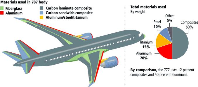
2 Quantum Hall Effect Linear Spectrum Transistors High Mobility? One Atom Thin Membranes/ Gas Barrier Strength Photovoltaics Composites Unique Optical Properties Highly Transparent Stretchable SPECTROSCOPY AND MATERIALS Conductors GROUP 2
3 Bendability of Electronic Materials Material Fracture Strain Material Fracture Strain Silicon ~0.7% Poly- ZnO 0.03% ITO 0.58~1.15% Polyimide 4% Au 0.46% Graphene >15-20%

4 How to Make Graphene? Drawing: ELECTRONIC DEVICES AND MATERIALS GROUP (micro) mechanical cleavage of graphite
5 How to Make Graphene? GRAPHITE IS STRONGLY LAYERED SLICE DOWN TO ONE ATOMIC PLANE ELECTRONIC DEVICES AND MATERIALS GROUP


6 Graphene Production


")

7 SKKU Process Bae Nature Nano (2010)


8 Industrial graphite purification & exfoliation 10

9 Chemical Exfoliation of Graphene Large area CAMBRIDGE graphene UNIVERSITY coverage 28 April
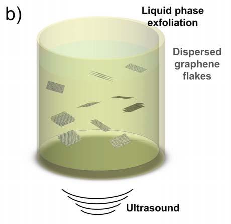
10 Liquid phase exfoliation graphite + Ultrasonication Ideal case: 100% monolayer graphene flakes
11 Liquid phase exfoliation Dispersion in organic solvent Dispersion in watersurfactant solution Solvent with high surface tension prevents re-aggregations! Surfactant compensates repulsion between water and graphene. Y. Hernandez et al. Nat. Nano. (2008) SPECTROSCOPY AND MATERIALS M. Lotya et al. JACS (2009) GROUP

12 14
13 TEM statistics Liquid phase exfoliation in water Number of flakes N= Number of layers Number of flakes N= Area (nm 2 ) Yield(monolayer)~70%
14 Sorting number of layers via Density Gradient Ultracentrifugation (DGU) Issue: Monolayer, bi-layer, trilayer have same density (ρ)! We exploit the effect of surfactant coverage
15 Sorting number of layers via DGU NOW: Density depends on number of layers After DGU ρ The buoyant density increase with N.. N-layers A. SPECTROSCOPY Green, AND MATERIALS M. Hersam, GROUP Nano lett. (2009)
16 Sorting number of layers via DGU D 2D D Raman shift (cm -1 )


17 Sorting number of layers via DGU 200 nm


18 Ink-Jet Printing Graphene-Ink


19 Deterministic Placement On Si/SiO 2 On Optical Fiber

20 BILAYER TWIST Overlap Bottom Intensity [A.U.] OVERLAP TOP Top BOTTOM Raman shift [cm-1]


/SiO 2")


21 Wafer Scale Graphene Transfer Mechanical Support/Graphene/Ni(or Cu)/SiO 2 peeling off in water Ni (or Cu) Rapid etching with FeCl 3 (aq) Graphene on polymer support Post-patterning SiO 2 Transfer Pre-patterning Patterned graphene on Ni Patterned graphene on arbitrary substrate Patterning Graphene on arbitrary substrate Kim et al Nature 2010


22 Wafer Scale Graphene Devices 16,200 FET devices L C : 10 μm L W : 5 μm Y. Lee et al. NanoLett., 10, 490 (2010)

23 Graphitic Carbon For LHC

24 Preparation for SPS magnet prototype graphitic coating


25 Gas barrier diffusion properties Gas Diffusion Barrier Barrier to oxygen Barrier to CO 2 gas CO 2 O 2 AA H 2 O Migration of flavors Industrial specifications compatible with blow molding production rate few seconds Deposition time Packaging regulation Recyclable food contact safe
 60 50 40 30 20 10 C 2 H 2 : 160")

26 Thickness distribution Uniformity = ± 15% Thickness (nm) C 2 H 2 : 160 sccm MWP: 350 W T1 : 1 s T2 : 1 s P1 : 50 mbars P2 : 0.1 mbars Point Vd = 60 nm/s
27 25,0 20,0 PET a-c:h 60 nm a-c:h : 150 nm CSD - CSD (17.5% of CO 2 loss) - 44 weeks with 60 nm a-c:h %CO2 Loss 15,0 10,0 Beer - 52 weeks with 150 nm a-c:h - Beer (10% of CO 2 loss) -25 weeks with 60 nm a-c:h -30 weeks with 150 nm a-c:h - Non coated PET bottle - 4 to 10 weeks shelf life 5,0 0,0 Shelf life (weeks) 0,0 10,0 20,0 30,0 Time (weeks) 40,0 50,0 60, Thickness(nm)


28 Bunch,McEuen, Nano Lett 2008 Graphene Balloon

29 Composites Strain Sensor


30 Optical micrograph Optical properties Confocal Rayleigh map Graphene can be visualized optically Casiraghi, C. et al Nano Lett. 7, 2711 (2007). The optical image contrast scales with the number of layers

31 Optical properties Universal optical conductance G 0 = e 2 /4ħ Ω 1 T = ( πα) 2 1 πα 97.7% A=1-T=πα=2.3% SLG reflects << 0.1% of the incident light in the visible region, raising to ~2% for 10 layers Nair Science 2008 Kuzmenko PRL 2008
32 ITO drawbacks Increasing cost due to Indium scarcity Processing requirements, difficulties in patterning Sensitivity to acidic and basic environments Brittleness Wear resistance
33 ITO replacements 100 Transmittance (%) ITO ZnO/Ag/ZnO TiO 2 /Ag/TiO 2 Arc discharge SWNTs Wavelength (nm) Metal grids, metallic nanowires, metal oxides and SWNTs have been explored as ITO alternative
34 100 Transmittance (%) Graphene ITO ZnO/Ag/ZnO TiO 2 /Ag/TiO 2 Arc discharge SWNTs Wavelength (nm) Graphene films have higher T over a wider wavelength range with respect to SWNT films, thin metallic films, and ITO
35 For n 0, σ dc,min 4e 2 /h R s 6kΩ/ for an ideal intrinsic SLG with T 97.7% Thus, ideal intrinsic SLG, would beat the best ITO only in terms of T, not R s
36 100 Transmittance (%) n=3.4x10 12 cm -2 μ=2x10 4 cm 2 / Vs R s (Ω/sq) LPE RGO PAHs CVD MC Graphene calc.

37
38 Graphene-based flexible smart window


39 Rod coating Graphene dispersion Rod coater PET film Wire winding Substrate Graphene dispersion

40 Transparent conductor On PET ~ 500Ω sheet resistance ~ 80% transparency


41 Polymer dispersed Liquid Crystal: Schematic Flexible, transparent Polymer support Polymer dispersed Liquid Crystal Graphene based transparent electrode Graphene based transparent electrode Polymer dispersed Liquid Crystal V V Flexible, transparent Polymer support

42 Touch screens The TC requirements for touch screens are R s Ω/ and T>90% Considering the R s and T required, GTCFs produced via LPE offer a viable way towards low cost devices


43 Wafer-Scale Synthesis and Transfer Transparent graphene film 4 inch scale graphene film on Stretchable Substrate Patterned GrapheneDEPARTMENT film OF 4 ENGINEERING inch scale graphene film SPECTROSCOPY AND on MATERIALS GROUP on PET Flexible Substrate
44
")
45 SKKU Touch screen Bae, S. et al. Nature Nano (2010)
 TFT OLED")

46 Flexible, Foldable AMOLED Display Touch Screen Anode (ITO) TFT OLED Cathode Substrate Front Plane : Touch Screen, OLED Back plane : TFTs

47
48 Photovoltaic devices Graphene can fulfil multiple functions in PV devices: 1) Transparent conductor window 2) Photoactive material 3) Channel for charge transport 4) Catalyst

49 Silicon solar cells Silicon solar cells dominate the current PV technology η up to ~25% Graphene TC Films can be used as window electrodes in inorganic solar cells
50 Organic solar cells Transparent conductor window Photoactive material η > 12% could be possible Yong, V.,Tour, J. M. Small 6, 313 (2009)
51 Dye Sensitized Solar Cell O'Regan and Gratzel, Nature, 252, 737 (1991) Transparent conductive electrode Graphene bridge structure I 3 - I - I - I 3 - Counter electrode

52 DSSCs assembly Graphene electrode is prepared by drop casting the dispersion on quartz substrate
53 Graphene based PDs (GPDs) Photodetectors Avouris, et al. GPDs can work over a much broader wavelength range GPDs have a faster response compared to traditional PDs
54 Graphene for photodetection high mobility and Fermi velocity potentially allow high operating speeds f t 40 GHz / 10 Gbit/s demonstrated absorption of 2.3 % per layer constant over the visible range to the infrared zero band-gap semiconductor no cut-off wavelength dark current Mueller et. al., Nature Photonics 4, 297 (2010). Nair et. al., Science 6, 5881 (2008).


55 Working principle e-h pair creation e-h Metal-induced separation doping Metal Giovanetti et. al., Phys. Rev. Lett. 101, (2008).

56 Light emitting devices Organic light emitting diodes (OLED) TC films based on graphene and graphene oxide have been demonstrated for OLED and light-emitting electrochemical cell Electroluminescence observed in graphene could lead to novel emitting devices based entirely on graphene Essig, S. et al. Nano Lett. 10, 1589 (2010)
57 Making Graphene Photoluminescent

58 3s, scale 5μm

59 PL Elastic Scattering

60
61 Broadband Nonlinear PL PL e-e relaxation (~100fs) Optical pumping Cooling by phonon emission (~1ps)


62 Broadband Nonlinear PL Elastic light scattering image Nonlinear PL image Red and Blue PL, as result of e-e collisions Heinz+Wang+Sthor+Hartschuh SPECTROSCOPY AND MATERIALS 50 x 50 µm GROUP 2
 laser into an ultrafast laser Mode-locked laser produces: Ultra-short Pulse Duration Enhanced Peak Power Wide")
63 Ultrafast lasers Mirror Mirror Laser gain media Saturable Absorber CW Ultrafast Pulses < second A saturable absorber turns a continuous wave (CW) laser into an ultrafast laser Mode-locked laser produces: Ultra-short Pulse Duration Enhanced Peak Power Wide Spectrum


64 Applications of mode-locked lasers Normal Cancerous CAMBRIDGE Essential UNIVERSITY tools for cutting-edge research in Physics, DEPARTMENT Engineering, OF ENGINEERING Chemistry, Biology, Nanotechnology
65 The effect of a saturable absorber First, imagine raster-scanning the pulse vs. time like this: Intensity Short time (fs) Round trips (k) k = 1 k = 2 k = 3 k = 7 After many round trips, even a slightly saturable absorber can yield a very short pulse. Notice that the weak pulses are suppressed, and the strong pulse shortens and is amplified.
66 Problems with current technology Current technology of Semiconductor Saturable Absorber Mirrors (SESAM) requires molecular beam epitaxy growth of GaInAs/GaAs heterostructures ion implantation (Ni, Be, etc) to reduce relaxation time can work only in reflective mode
67 Graphene as an ultrafast ultrawide band saturable absorber e-e relaxation (~100fs) Cooling by phonon emission (~1ps) Optical pumping
68 Exploiting the wide graphene absorption band: Wavelength tunability Graphene Normalized Intensity nm 1534nm 1541nm 1547nm 1553nm 1559nm Absorbance (a.u.) CNTs Wavelength (nm) Wavelength (nm) Wavelength (nm) Z. Sun et al. Nano Research (2010) 70

69 Ultrafast laser Graphene-SMMA polymer composite Highly-doped Er 3+ fiber WDM Pump laser ISO Coupler PC Output Graphene mode-locker SPECTROSCOPY AND Z. Sun MATERIALS et al. ACS GROUP nano 4, 803, 2010

70 Graphene Mode-locked Laser

71 Wavelength-tuneable Graphene Mode-locked Laser
72 Quantum Hall Effect Linear Spectrum Transistors High Mobility? One Atom Thin Membranes/ Gas Barrier Strength Photovoltaics Composites Unique Optical Properties Highly Transparent Stretchable SPECTROSCOPY AND MATERIALS Conductors GROUP 74


73 Potential of Graphene Flexible Display Touch Panel Conductive ink EMI screen ink High speed Transistor RFIC, Sensor Graphene Dispaly /Solar cell Packag Solar cell Battery Supercap. LEDlighting, BLU Automobile ECU PC Automobile Air plane components Science Engineering Technology
74
75 D.M. Basko E. Lidorikis A.Hartschuh H. Qian T. Gokus T. Ryhanen S. Lacour J. Kivioja A. Colli P. Beecher Z. Radivojevic P. Chiggiato M. Taborelli Thanks to K. S. Novoselov A. K. Geim Jong-Hyun Ahn Byung Hee Hong A. Lombardo B. Bonetti T.J. Echtermeyer Z. Sun D. Popa S. Piscanec F. Bonaccorso G. Calogero T. Hasan G. Privitera F. Torrisi T. M. G. Mohiuddin R. R. Nair C. Galiotis


76 Acknowledgements
Session V: Graphene. Matteo Bruna CAMBRIDGE UNIVERSITY DEPARTMENT OF ENGINEERING
 Session V: Graphene Matteo Bruna Graphene: Material in the Flatland Graphite Graphene Properties: Thinnest imaginable material Good(and tunable) electrical conductor Strongest ever measured Stiffest known
ULTRA-SHORT OPTICAL PULSE GENERATION WITH SINGLE-LAYER GRAPHENE
 Journal of Nonlinear Optical Physics & Materials Vol. 19, No. 4 (2010) 767 771 c World Scientific Publishing Company DOI: 10.1142/S021886351000573X ULTRA-SHORT OPTICAL PULSE GENERATION WITH SINGLE-LAYER
Wafer-scale fabrication of graphene
 Wafer-scale fabrication of graphene Sten Vollebregt, MSc Delft University of Technology, Delft Institute of Mircosystems and Nanotechnology Delft University of Technology Challenge the future Delft University
Supporting Information. Fast Synthesis of High-Performance Graphene by Rapid Thermal Chemical Vapor Deposition
 1 Supporting Information Fast Synthesis of High-Performance Graphene by Rapid Thermal Chemical Vapor Deposition Jaechul Ryu, 1,2, Youngsoo Kim, 4, Dongkwan Won, 1 Nayoung Kim, 1 Jin Sung Park, 1 Eun-Kyu
Efficient Preparation of Large-Area Graphene Oxide Sheets for Transparent Conductive Films
 Supporting Information Efficient Preparation of Large-Area Graphene Oxide Sheets for Transparent Conductive Films Jinping Zhao, Songfeng Pei, Wencai Ren*, Libo Gao and Hui-Ming Cheng* Shenyang National
Overview. Carbon in all its forms. Background & Discovery Fabrication. Important properties. Summary & References. Overview of current research
 Graphene Prepared for Solid State Physics II Pr Dagotto Spring 2009 Laurene Tetard 03/23/09 Overview Carbon in all its forms Background & Discovery Fabrication Important properties Overview of current
Transparent Electrode Applications
 Transparent Electrode Applications LCD Solar Cells Touch Screen Indium Tin Oxide (ITO) Zinc Oxide (ZnO) - High conductivity - High transparency - Resistant to environmental effects - Rare material (Indium)
Graphene Based Saturable Absorber Modelockers at 2µm
 ISLA Workshop Munich Integrated disruptive components for 2µm fibre Lasers ISLA Graphene Based Saturable Absorber Modelockers at 2µm Prof. Werner Blau - Trinity College Dublin Friday, 26th of June 2015
Development of active inks for organic photovoltaics: state-of-the-art and perspectives
 Development of active inks for organic photovoltaics: state-of-the-art and perspectives Jörg Ackermann Centre Interdisciplinaire de Nanoscience de Marseille (CINAM) CNRS - UPR 3118, MARSEILLE - France
2011 GCEP Report. Project title: Self-sorting of Carbon Nanotubes for High Performance Large Area Transparent Electrodes for Solar Cells
 2011 GCEP Report Project title: Self-sorting of Carbon Nanotubes for High Performance Large Area Transparent Electrodes for Solar Cells Investigators Zhenan Bao, Associate Professor, Chemical Engineering
CVD growth of Graphene. SPE ACCE presentation Carter Kittrell James M. Tour group September 9 to 11, 2014
 CVD growth of Graphene SPE ACCE presentation Carter Kittrell James M. Tour group September 9 to 11, 2014 Graphene zigzag armchair History 1500: Pencil-Is it made of lead? 1789: Graphite 1987: The first
Supplementary material for High responsivity mid-infrared graphene detectors with antenna-enhanced photo-carrier generation and collection
 Supplementary material for High responsivity mid-infrared graphene detectors with antenna-enhanced photo-carrier generation and collection Yu Yao 1, Raji Shankar 1, Patrick Rauter 1, Yi Song 2, Jing Kong
Graphene Fundamentals and Emergent Applications
 Graphene Fundamentals and Emergent Applications Jamie H. Warner Department of Materials University of Oxford Oxford, UK Franziska Schaffel Department of Materials University of Oxford Oxford, UK Alicja
Flexible Organic Photovoltaics Employ laser produced metal nanoparticles into the absorption layer 1. An Introduction
 Flexible Organic Photovoltaics Employ laser produced metal nanoparticles into the absorption layer 1. An Introduction Among the renewable energy sources that are called to satisfy the continuously increased
OPTI510R: Photonics. Khanh Kieu College of Optical Sciences, University of Arizona Meinel building R.626
 OPTI510R: Photonics Khanh Kieu College of Optical Sciences, University of Arizona kkieu@optics.arizona.edu Meinel building R.626 Announcements Homework #6 is assigned, due May 1 st Final exam May 8, 10:30-12:30pm
Quantum Dots for Advanced Research and Devices
 Quantum Dots for Advanced Research and Devices spectral region from 450 to 630 nm Zero-D Perovskite Emit light at 520 nm ABOUT QUANTUM SOLUTIONS QUANTUM SOLUTIONS company is an expert in the synthesis
Plastic Electronics. Joaquim Puigdollers.
 Plastic Electronics Joaquim Puigdollers Joaquim.puigdollers@upc.edu Nobel Prize Chemistry 2000 Origins Technological Interest First products.. MONOCROMATIC PHILIPS Today Future Technological interest Low
FMM, 15 th Feb Simon Zihlmann
 FMM, 15 th Feb. 2013 Simon Zihlmann Outline Motivation Basics about graphene lattice and edges Introduction to Raman spectroscopy Scattering at the edge Polarization dependence Thermal rearrangement of
30-Inch Roll-Based Production of High-Quality Graphene Films for Flexible Transparent Electrodes
 30-Inch Roll-Based Production of High-Quality Graphene Films for Flexible Transparent Electrodes Sukang Bae, 1* Hyeong Keun Kim, 3* Xianfang Xu, 5 Jayakumar Balakrishnan, 5 Tian Lei, 1 Young Il Song, 6
Graphene. Tianyu Ye November 30th, 2011
 Graphene Tianyu Ye November 30th, 2011 Outline What is graphene? How to make graphene? (Exfoliation, Epitaxial, CVD) Is it graphene? (Identification methods) Transport properties; Other properties; Applications;
Initial Stages of Growth of Organic Semiconductors on Graphene
 Initial Stages of Growth of Organic Semiconductors on Graphene Presented by: Manisha Chhikara Supervisor: Prof. Dr. Gvido Bratina University of Nova Gorica Outline Introduction to Graphene Fabrication
Supplementary Figure 1. Selected area electron diffraction (SAED) of bilayer graphene and tblg. (a) AB
 of bilayer graphene and tblg. (a) AB") Supplementary Figure 1. Selected area electron diffraction (SAED) of bilayer graphene and tblg. (a) AB stacked bilayer graphene (b), (c), (d), (e), and (f) are twisted bilayer graphene with twist angle
Supplementary Figure 1. Selected area electron diffraction (SAED) of bilayer graphene and tblg. (a) AB stacked bilayer graphene (b), (c), (d), (e), and (f) are twisted bilayer graphene with twist angle
Stretchable Graphene Transistors with Printed Dielectrics and Gate Electrodes
 Stretchable Graphene Transistors with Printed Dielectrics and Gate Electrodes Seoung-Ki Lee, Beom Joon Kim, Houk Jang, Sung Cheol Yoon, Changjin Lee, Byung Hee Hong, John A. Rogers, Jeong Ho Cho, Jong-Hyun
graphene nano-optoelectronics Frank Koppens ICFO, The institute of photonic sciences, Barcelona
 graphene nano-optoelectronics Frank Koppens ICFO, The institute of photonic sciences, Barcelona Graphene research at ICFO Frank Koppens: group Nano-optoelectronics (~100% graphene) Nano-optics and plasmonics
Figure 1: Graphene release, transfer and stacking processes. The graphene stacking began with CVD
 Supplementary figure 1 Graphene Growth and Transfer Graphene PMMA FeCl 3 DI water Copper foil CVD growth Back side etch PMMA coating Copper etch in 0.25M FeCl 3 DI water rinse 1 st transfer DI water 1:10
Seminars in Nanosystems - I
 Seminars in Nanosystems - I Winter Semester 2011/2012 Dr. Emanuela Margapoti Emanuela.Margapoti@wsi.tum.de Dr. Gregor Koblmüller Gregor.Koblmueller@wsi.tum.de Seminar Room at ZNN 1 floor Topics of the
2D MBE Activities in Sheffield. I. Farrer, J. Heffernan Electronic and Electrical Engineering The University of Sheffield
 2D MBE Activities in Sheffield I. Farrer, J. Heffernan Electronic and Electrical Engineering The University of Sheffield Outline Motivation Van der Waals crystals The Transition Metal Di-Chalcogenides
2D Materials for Gas Sensing
 2D Materials for Gas Sensing S. Guo, A. Rani, and M.E. Zaghloul Department of Electrical and Computer Engineering The George Washington University, Washington DC 20052 Outline Background Structures of
Carbon Nanomaterials: Nanotubes and Nanobuds and Graphene towards new products 2030
 Carbon Nanomaterials: Nanotubes and Nanobuds and Graphene towards new products 2030 Prof. Dr. Esko I. Kauppinen Helsinki University of Technology (TKK) Espoo, Finland Forecast Seminar February 13, 2009
Carbon Nanotubes in Interconnect Applications
 Carbon Nanotubes in Interconnect Applications Page 1 What are Carbon Nanotubes? What are they good for? Why are we interested in them? - Interconnects of the future? Comparison of electrical properties
TRANSVERSE SPIN TRANSPORT IN GRAPHENE
 International Journal of Modern Physics B Vol. 23, Nos. 12 & 13 (2009) 2641 2646 World Scientific Publishing Company TRANSVERSE SPIN TRANSPORT IN GRAPHENE TARIQ M. G. MOHIUDDIN, A. A. ZHUKOV, D. C. ELIAS,
Monolithic Cells for Solar Fuels
 Electronic Supplementary Material (ESI) for Chemical Society Reviews. This journal is The Royal Society of Chemistry 2014 Monolithic Cells for Solar Fuels Jan Rongé, Tom Bosserez, David Martel, Carlo Nervi,
Plasmonic Hot Hole Generation by Interband Transition in Gold-Polyaniline
 Supplementary Information Plasmonic Hot Hole Generation by Interband Transition in Gold-Polyaniline Tapan Barman, Amreen A. Hussain, Bikash Sharma, Arup R. Pal* Plasma Nanotech Lab, Physical Sciences Division,
Supporting Information Available:
 Supporting Information Available: Photoresponsive and Gas Sensing Field-Effect Transistors based on Multilayer WS 2 Nanoflakes Nengjie Huo 1, Shengxue Yang 1, Zhongming Wei 2, Shu-Shen Li 1, Jian-Bai Xia
Optical Spectroscopy of Advanced Materials
 Phys 590B Condensed Matter Physics: Experimental Methods Optical Spectroscopy of Advanced Materials Basic optics, nonlinear and ultrafast optics Jigang Wang Department of Physics, Iowa State University
Graphene photodetectors with ultra-broadband and high responsivity at room temperature
 SUPPLEMENTARY INFORMATION DOI: 10.1038/NNANO.2014.31 Graphene photodetectors with ultra-broadband and high responsivity at room temperature Chang-Hua Liu 1, You-Chia Chang 2, Ted Norris 1.2* and Zhaohui
vapour deposition. Raman peaks of the monolayer sample grown by chemical vapour
 Supplementary Figure 1 Raman spectrum of monolayer MoS 2 grown by chemical vapour deposition. Raman peaks of the monolayer sample grown by chemical vapour deposition (S-CVD) are peak which is at 385 cm
Ultrafast Electron-Electron Dynamics in Graphene Daniele Brida
 Ultrafast Electron-Electron Dynamics in Graphene Ultrafast Spectroscopy Light-matter interaction on timescale of fundamental physical processes: electron scattering, phonon emission, energy transfer D.
Mesoporous titanium dioxide electrolyte bulk heterojunction
 Mesoporous titanium dioxide electrolyte bulk heterojunction The term "bulk heterojunction" is used to describe a heterojunction composed of two different materials acting as electron- and a hole- transporters,
Carbon Nanotube Thin-Films & Nanoparticle Assembly
 Nanodevices using Nanomaterials : Carbon Nanotube Thin-Films & Nanoparticle Assembly Seung-Beck Lee Division of Electronics and Computer Engineering & Department of Nanotechnology, Hanyang University,
Optically-Pumped Ge-on-Si Gain Media: Lasing and Broader Impact
 Optically-Pumped Ge-on-Si Gain Media: Lasing and Broader Impact J. Liu 1, R. Camacho 2, X. Sun 2, J. Bessette 2, Y. Cai 2, X. X. Wang 1, L. C. Kimerling 2 and J. Michel 2 1 Thayer School, Dartmouth College;
The Electromagnetic Properties of Materials
 The Electromagnetic Properties of Materials Electrical conduction Metals Semiconductors Insulators (dielectrics) Superconductors Magnetic materials Ferromagnetic materials Others Photonic Materials (optical)
Graphene films on silicon carbide (SiC) wafers supplied by Nitride Crystals, Inc.
 wafers supplied by Nitride Crystals, Inc.") 9702 Gayton Road, Suite 320, Richmond, VA 23238, USA Phone: +1 (804) 709-6696 info@nitride-crystals.com www.nitride-crystals.com Graphene films on silicon carbide (SiC) wafers supplied by Nitride Crystals,
9702 Gayton Road, Suite 320, Richmond, VA 23238, USA Phone: +1 (804) 709-6696 info@nitride-crystals.com www.nitride-crystals.com Graphene films on silicon carbide (SiC) wafers supplied by Nitride Crystals,
SUPPLEMENTARY INFORMATION
 SUPPLEMENTARY INFORMATION Facile Synthesis of High Quality Graphene Nanoribbons Liying Jiao, Xinran Wang, Georgi Diankov, Hailiang Wang & Hongjie Dai* Supplementary Information 1. Photograph of graphene
Lectures Graphene and
 Lectures 15-16 Graphene and carbon nanotubes Graphene is atomically thin crystal of carbon which is stronger than steel but flexible, is transparent for light, and conducts electricity (gapless semiconductor).
SUPPLEMENTARY INFORMATION
 SUPPLEMENTARY INFORMATION I. Experimental Thermal Conductivity Data Extraction Mechanically exfoliated graphene flakes come in different shape and sizes. In order to measure thermal conductivity of the
photonic crystals School of Space Science and Physics, Shandong University at Weihai, Weihai , China
 Enhanced absorption in heterostructures with graphene and truncated photonic crystals Yiping Liu 1, Lei Du 1, Yunyun Dai 2, Yuyu Xia 2, Guiqiang Du 1,* Guang Lu 1, Fen Liu 1, Lei Shi 2, Jian Zi 2 1 School
Graphene Novel Material for Nanoelectronics
 Graphene Novel Material for Nanoelectronics Shintaro Sato Naoki Harada Daiyu Kondo Mari Ohfuchi (Manuscript received May 12, 2009) Graphene is a flat monolayer of carbon atoms with a two-dimensional honeycomb
Graphene Canada Montreal Oct. 16, 2015 (International Year of Light)
") Luminescence Properties of Graphene A. Beltaos 1,2,3, A. Bergren 1, K. Bosnick 1, N. Pekas 1, A. Matković 4, A. Meldrum 2 1 National Institute for Nanotechnology (NINT), 11421 Saskatchewan Drive, Edmonton,
Luminescence Properties of Graphene A. Beltaos 1,2,3, A. Bergren 1, K. Bosnick 1, N. Pekas 1, A. Matković 4, A. Meldrum 2 1 National Institute for Nanotechnology (NINT), 11421 Saskatchewan Drive, Edmonton,
1. Nanotechnology & nanomaterials -- Functional nanomaterials enabled by nanotechnologies.
 Novel Nano-Engineered Semiconductors for Possible Photon Sources and Detectors NAI-CHANG YEH Department of Physics, California Institute of Technology 1. Nanotechnology & nanomaterials -- Functional nanomaterials
Semiconductor Disk Laser on Microchannel Cooler
 Semiconductor Disk Laser on Microchannel Cooler Eckart Gerster An optically pumped semiconductor disk laser with a double-band Bragg reflector mirror is presented. This mirror not only reflects the laser
Carbon Nanomaterials
 Carbon Nanomaterials STM Image 7 nm AFM Image Fullerenes C 60 was established by mass spectrographic analysis by Kroto and Smalley in 1985 C 60 is called a buckminsterfullerene or buckyball due to resemblance
Ultrafast Lateral Photo-Dember Effect in Graphene. Induced by Nonequilibrium Hot Carrier Dynamics
 1 Ultrafast Lateral Photo-Dember Effect in Graphene Induced by Nonequilibrium Hot Carrier Dynamics Chang-Hua Liu, You-Chia Chang, Seunghyun Lee, Yaozhong Zhang, Yafei Zhang, Theodore B. Norris,*,, and
Raman spectroscopy at the edges of multilayer graphene
 Raman spectroscopy at the edges of multilayer graphene Q. -Q. Li, X. Zhang, W. -P. Han, Y. Lu, W. Shi, J. -B. Wu, P. -H. Tan* State Key Laboratory of Superlattices and Microstructures, Institute of Semiconductors,
Nanostructures. Lecture 13 OUTLINE
 Nanostructures MTX9100 Nanomaterials Lecture 13 OUTLINE -What is quantum confinement? - How can zero-dimensional materials be used? -What are one dimensional structures? -Why does graphene attract so much
Generation of photovoltage in graphene on a femtosecond timescale through efficient carrier heating
 DOI: 1.138/NNANO.215.54 Generation of photovoltage in graphene on a femtosecond timescale through efficient carrier heating K. J. Tielrooij, L. Piatkowski, M. Massicotte, A. Woessner, Q. Ma, Y. Lee, K.
Nanomaterials & Organic Electronics Group TEI of Crete
 Nanomaterials & Organic Electronics Group TEI of Crete Dr. Emmanuel Kymakis Asc. Professor, Dept. of Electrical Engineering and Center of Advanced Materials & Photonics kymakis@staff.teicrete.gr http://nano.teicrete.gr/
(Co-PIs-Mark Brongersma, Yi Cui, Shanhui Fan) Stanford University. GCEP Research Symposium 2013 Stanford, CA October 9, 2013
 Stanford University. GCEP Research Symposium 2013 Stanford, CA October 9, 2013") High-efficiency thin film nano-structured multi-junction solar James S. cells Harris (PI) (Co-PIs-Mark Brongersma, Yi Cui, Shanhui Fan) Stanford University GCEP Research Symposium 2013 Stanford, CA October
High-efficiency thin film nano-structured multi-junction solar James S. cells Harris (PI) (Co-PIs-Mark Brongersma, Yi Cui, Shanhui Fan) Stanford University GCEP Research Symposium 2013 Stanford, CA October
UNIT I: Electronic Materials.
 SIDDHARTH INSTITUTE OF ENGINEERING & TECHNOLOGY :: PUTTUR Siddharth Nagar, Narayanavanam Road 517583 QUESTION BANK (DESCRIPTIVE) Subject with Code: SEMICONDUCTOR PHYSICS (18HS0851) Course & Branch: B.Tech
Scalable Nanomaterials and Nanostructures for Energy and Flexible Electronics
 Scalable Nanomaterials and Nanostructures for Energy and Flexible Electronics Liangbing (Bing) Hu MSE & Energy Center University of Maryland College Park Email: binghu@umd.edu 1 Transparent Paper from
Tunneling characteristics of graphene
 Tunneling characteristics of graphene Young Jun Shin, 1,2 Gopinadhan Kalon, 1,2 Jaesung Son, 1 Jae Hyun Kwon, 1,2 Jing Niu, 1 Charanjit S. Bhatia, 1 Gengchiau Liang, 1 and Hyunsoo Yang 1,2,a) 1 Department
Title: Ultrafast photocurrent measurement of the escape time of electrons and holes from
 Title: Ultrafast photocurrent measurement of the escape time of electrons and holes from carbon nanotube PN junction photodiodes Authors: Nathaniel. M. Gabor 1,*, Zhaohui Zhong 2, Ken Bosnick 3, Paul L.
A. Optimizing the growth conditions of large-scale graphene films
 1 A. Optimizing the growth conditions of large-scale graphene films Figure S1. Optical microscope images of graphene films transferred on 300 nm SiO 2 /Si substrates. a, Images of the graphene films grown
High Power Diode Lasers
 Lecture 10/1 High Power Diode Lasers Low Power Lasers (below tenth of mw) - Laser as a telecom transmitter; - Laser as a spectroscopic sensor; - Laser as a medical diagnostic tool; - Laser as a write-read
Nanocomposite photonic crystal devices
 Nanocomposite photonic crystal devices Xiaoyong Hu, Cuicui Lu, Yulan Fu, Yu Zhu, Yingbo Zhang, Hong Yang, Qihuang Gong Department of Physics, Peking University, Beijing, P. R. China Contents Motivation
Supporting Information: Poly(dimethylsiloxane) Stamp Coated with a. Low-Surface-Energy, Diffusion-Blocking,
 Stamp Coated with a. Low-Surface-Energy, Diffusion-Blocking,") Supporting Information: Poly(dimethylsiloxane) Stamp Coated with a Low-Surface-Energy, Diffusion-Blocking, Covalently Bonded Perfluoropolyether Layer and Its Application to the Fabrication of Organic Electronic
Supporting Information: Poly(dimethylsiloxane) Stamp Coated with a Low-Surface-Energy, Diffusion-Blocking, Covalently Bonded Perfluoropolyether Layer and Its Application to the Fabrication of Organic Electronic
Transient Photocurrent Measurements of Graphene Related Materials
 Transient Photocurrent Measurements of Graphene Related Materials P. Srinivasa Rao Mentor: Prof. dr. Gvido Bratina Laboratory of Organic Matter Physics University of Nova Gorica 1 Contents: 1. Electrical
Nanostrukturphysik (Nanostructure Physics)
") Nanostrukturphysik (Nanostructure Physics) Prof. Yong Lei & Dr. Yang Xu Fachgebiet 3D-Nanostrukturierung, Institut für Physik Contact: yong.lei@tu-ilmenau.de; yang.xu@tu-ilmenau.de Office: Unterpoerlitzer
Nanostrukturphysik (Nanostructure Physics) Prof. Yong Lei & Dr. Yang Xu Fachgebiet 3D-Nanostrukturierung, Institut für Physik Contact: yong.lei@tu-ilmenau.de; yang.xu@tu-ilmenau.de Office: Unterpoerlitzer
Electrical Conductive Adhesives with Nanotechnologies
 Yi Li Daniel Lu C.P. Wong Electrical Conductive Adhesives with Nanotechnologies Springer 1 Introduction 1 1.1 Electronics Packaging and Interconnect 1 1.2 Interconnection Materials 11 1.2.1 Lead-Free Interconnect
Metal Vapour Lasers Use vapoured metal as a gain medium Developed by W. Silfvast (1966) Two types: Ionized Metal vapour (He-Cd) Neutral Metal vapour
 Two types: Ionized Metal vapour (He-Cd) Neutral Metal vapour") Metal Vapour Lasers Use vapoured metal as a gain medium Developed by W. Silfvast (1966) Two types: Ionized Metal vapour (He-Cd) Neutral Metal vapour (Cu) All operate by vaporizing metal in container Helium
Metal Vapour Lasers Use vapoured metal as a gain medium Developed by W. Silfvast (1966) Two types: Ionized Metal vapour (He-Cd) Neutral Metal vapour (Cu) All operate by vaporizing metal in container Helium
Processing and Applications of Carbon Nanotubes, Graphene, and Beyond
 Processing and Applications of Carbon Nanotubes, Graphene, and Beyond Professor Mark C. Hersam Department of Materials Science and Engineering Northwestern University http://www.hersam-group.northwestern.edu/
TECHNICAL INFORMATION. Quantum Dot
 Quantum Dot Quantum Dot is the nano meter sized semiconductor crystal with specific optical properties originates from the phenomenon which can be explained by the quantum chemistry and quantum mechanics.
Ultrafast single photon emitting quantum photonic structures. based on a nano-obelisk
 Ultrafast single photon emitting quantum photonic structures based on a nano-obelisk Je-Hyung Kim, Young-Ho Ko, Su-Hyun Gong, Suk-Min Ko, Yong-Hoon Cho Department of Physics, Graduate School of Nanoscience
R&D Achievements. Nano Material / Metal Parts
 R&D Achievements Nano Material / Metal Parts Organic/Inorganic Nano-hybrid Material Technology Hybrid varnish Acryl Resin/Silica Hybrid Varnish Kang Dong-pil +82-55-280-1610 dpkang@keri.re.kr Sol-gel Reactor
Nanomaterials for breakthrough innovations
 Nanomaterials for breakthrough innovations G. Fiori Dipartimento di Ingegneria dell Informazione, University of Pisa Via Caruso 16, 56122, Pisa, Italy. gfiori@mercurio.iet.unipi.it http://gianlucafiori.org
Electrochemically Synthesized Multi-block
 Electrochemically Synthesized Multi-block Nanorods Sungho Park SungKyunKwan University, Department of Chemistry & SKKU Advanced Institute of Nanotechnology (SAINT) J. Am. Chem. Soc. 2003, 125, 2282-2290
Q. Shen 1,2) and T. Toyoda 1,2)
 and T. Toyoda 1,2)") Photosensitization of nanostructured TiO 2 electrodes with CdSe quntum dots: effects of microstructure in substrates Q. Shen 1,2) and T. Toyoda 1,2) Department of Applied Physics and Chemistry 1), and
Photosensitization of nanostructured TiO 2 electrodes with CdSe quntum dots: effects of microstructure in substrates Q. Shen 1,2) and T. Toyoda 1,2) Department of Applied Physics and Chemistry 1), and
Thermal Transport in Graphene and other Two-Dimensional Systems. Li Shi. Department of Mechanical Engineering & Texas Materials Institute
 Thermal Transport in Graphene and other Two-Dimensional Systems Li Shi Department of Mechanical Engineering & Texas Materials Institute Outline Thermal Transport Theories and Simulations of Graphene Raman
Beatrice Beyer ISFOE 2014 Thessaloniki, Greece
 Beatrice Beyer ISFOE 2014 Thessaloniki, Greece What? Graphene which is both highly conductive and transparent Large volume production Process safety Proof of concept for use as transparent electrode Why?
Nanostrukturphysik Übung 2 (Class 3&4)
") Nanostrukturphysik Übung 2 (Class 3&4) Prof. Yong Lei & Dr. Yang Xu 2017.05.03 Fachgebiet 3D-Nanostrukturierung, Institut für Physik Contact: yong.lei@tu-ilmenau.de (3748), yang.xu@tuilmenau.de (4902)
Nanostrukturphysik Übung 2 (Class 3&4) Prof. Yong Lei & Dr. Yang Xu 2017.05.03 Fachgebiet 3D-Nanostrukturierung, Institut für Physik Contact: yong.lei@tu-ilmenau.de (3748), yang.xu@tuilmenau.de (4902)
OPTI510R: Photonics. Khanh Kieu College of Optical Sciences, University of Arizona Meinel building R.626
 OPTI510R: Photonics Khanh Kieu College of Optical Sciences, University of Arizona kkieu@optics.arizona.edu Meinel building R.626 Announcements HW#3 is assigned due Feb. 20 st Mid-term exam Feb 27, 2PM
Fermi Level Pinning at Electrical Metal Contacts. of Monolayer Molybdenum Dichalcogenides
 Supporting information Fermi Level Pinning at Electrical Metal Contacts of Monolayer Molybdenum Dichalcogenides Changsik Kim 1,, Inyong Moon 1,, Daeyeong Lee 1, Min Sup Choi 1, Faisal Ahmed 1,2, Seunggeol
Light Interaction with Small Structures
 Light Interaction with Small Structures Molecules Light scattering due to harmonically driven dipole oscillator Nanoparticles Insulators Rayleigh Scattering (blue sky) Semiconductors...Resonance absorption
Nonlinear ultrafast fiber optic devices based on Carbon Nanotubes
 Nonlinear ultrafast fiber optic devices based on Carbon Nanotubes Guillermo E. Villanueva, Claudio J. Oton Michael B. Jakubinek, Benoit Simard,, Jaques Albert, Pere Pérez-Millán Outline Introduction CNT-coated
Use of Multi-Walled Carbon Nanotubes for UV radiation detection
 Use of Multi-Walled Carbon Nanotubes for UV radiation detection Viviana Carillo 11th Topical Seminar on Innovative Particle and Radiation Detectors (IPRD08) 1-4 October 2008 Siena, Italy A new nanostructured
Ultrafast hot-carrier-dominated photocurrent in graphene
 SUPPLEMENTARY INFORMATION DOI: 10.1038/NNANO.2011.243 Ultrafast hot-carrier-dominated photocurrent in graphene Table of Contents: Dong Sun 1, Grant Aivazian 1, Aaron M. Jones 1, Jason S. Ross 2,Wang Yao
PHOTOVOLTAICS Fundamentals
 PHOTOVOLTAICS Fundamentals PV FUNDAMENTALS Semiconductor basics pn junction Solar cell operation Design of silicon solar cell SEMICONDUCTOR BASICS Allowed energy bands Valence and conduction band Fermi
There's Plenty of Room at the Bottom
 There's Plenty of Room at the Bottom 12/29/1959 Feynman asked why not put the entire Encyclopedia Britannica (24 volumes) on a pin head (requires atomic scale recording). He proposed to use electron microscope
Highly Efficient and Anomalous Charge Transfer in van der Waals Trilayer Semiconductors
 Highly Efficient and Anomalous Charge Transfer in van der Waals Trilayer Semiconductors Frank Ceballos 1, Ming-Gang Ju 2 Samuel D. Lane 1, Xiao Cheng Zeng 2 & Hui Zhao 1 1 Department of Physics and Astronomy,
The Effects of Hydrazine Monohydrate Surface Doping on Graphene
 Macalester Journal of Physics and Astronomy Volume 4 Issue 1 Spring 2016 Article 8 May 2016 The Effects of Hydrazine Monohydrate Surface Doping on Graphene Christian M. Stewart Macalester College, cstewart@macalester.edu
NANO TECHNOLOGY IN POLYMER SOLAR CELLS. Mayur Padharia, Hardik Panchal, Keval Shah, *Neha Patni, Shibu.G.Pillai
 NANO TECHNOLOGY IN POLYMER SOLAR CELLS Mayur Padharia, Hardik Panchal, Keval Shah, *Neha Patni, Shibu.G.Pillai Department of Chemical Engineering, Institute of Technology, Nirma University, S. G. Highway,
Semiconductor Optoelectronics Prof. M. R. Shenoy Department of Physics Indian Institute of Technology, Delhi
 Semiconductor Optoelectronics Prof. M. R. Shenoy Department of Physics Indian Institute of Technology, Delhi Lecture - 1 Context and Scope of the Course (Refer Slide Time: 00:44) Welcome to this course
Supplementary Figure 1 Dark-field optical images of as prepared PMMA-assisted transferred CVD graphene films on silicon substrates (a) and the one
 and the one") Supplementary Figure 1 Dark-field optical images of as prepared PMMA-assisted transferred CVD graphene films on silicon substrates (a) and the one after PBASE monolayer growth (b). 1 Supplementary Figure
Supplementary Figure 1 Dark-field optical images of as prepared PMMA-assisted transferred CVD graphene films on silicon substrates (a) and the one after PBASE monolayer growth (b). 1 Supplementary Figure
A new method of growing graphene on Cu by hydrogen etching
 A new method of growing graphene on Cu by hydrogen etching Linjie zhan version 6, 2015.05.12--2015.05.24 CVD graphene Hydrogen etching Anisotropic Copper-catalyzed Highly anisotropic hydrogen etching method
III-V nanostructured materials synthesized by MBE droplet epitaxy
 III-V nanostructured materials synthesized by MBE droplet epitaxy E.A. Anyebe 1, C. C. Yu 1, Q. Zhuang 1,*, B. Robinson 1, O Kolosov 1, V. Fal ko 1, R. Young 1, M Hayne 1, A. Sanchez 2, D. Hynes 2, and
Scaling up Chemical Vapor Deposition Graphene to 300 mm Si substrates
 Scaling up Chemical Vapor Deposition Graphene to 300 mm Si substrates Co- Authors Aixtron Alex Jouvray Simon Buttress Gavin Dodge Ken Teo The work shown here has received partial funding from the European
OPTICAL PROPERTIES AND SPECTROSCOPY OF NANOAAATERIALS. Jin Zhong Zhang. World Scientific TECHNISCHE INFORMATIONSBIBLIOTHEK
 OPTICAL PROPERTIES AND SPECTROSCOPY OF NANOAAATERIALS Jin Zhong Zhang University of California, Santa Cruz, USA TECHNISCHE INFORMATIONSBIBLIOTHEK Y World Scientific NEW JERSEY. t'on.don SINGAPORE «'BEIJING
Supplementary Figure 2 Photoluminescence in 1L- (black line) and 7L-MoS 2 (red line) of the Figure 1B with illuminated wavelength of 543 nm.
 and 7L-MoS 2 (red line) of the Figure 1B with illuminated wavelength of 543 nm.") PL (normalized) Intensity (arb. u.) 1 1 8 7L-MoS 1L-MoS 6 4 37 38 39 4 41 4 Raman shift (cm -1 ) Supplementary Figure 1 Raman spectra of the Figure 1B at the 1L-MoS area (black line) and 7L-MoS area (red
PL (normalized) Intensity (arb. u.) 1 1 8 7L-MoS 1L-MoS 6 4 37 38 39 4 41 4 Raman shift (cm -1 ) Supplementary Figure 1 Raman spectra of the Figure 1B at the 1L-MoS area (black line) and 7L-MoS area (red
SUPPLEMENTARY INFORMATION
 SUPPLEMENTARY INFORMATION DOI: 10.1038/NNANO.2011.123 Ultra-strong Adhesion of Graphene Membranes Steven P. Koenig, Narasimha G. Boddeti, Martin L. Dunn, and J. Scott Bunch* Department of Mechanical Engineering,
Nanostrukturphysik (Nanostructure Physics)
") Nanostrukturphysik (Nanostructure Physics) Prof. Yong Lei & Dr. Yang Xu Fachgebiet 3D-Nanostrukturierung, Institut für Physik Contact: yong.lei@tu-ilmenau.de; yang.xu@tu-ilmenau.de Office: Unterpoerlitzer
Nanostrukturphysik (Nanostructure Physics) Prof. Yong Lei & Dr. Yang Xu Fachgebiet 3D-Nanostrukturierung, Institut für Physik Contact: yong.lei@tu-ilmenau.de; yang.xu@tu-ilmenau.de Office: Unterpoerlitzer