Molecular and carbon-based electronic systems
|
|
|
- Ronald Simon
- 5 years ago
- Views:
Transcription
1 Molecular and carbon-based electronic systems when Wednesday, 10h15-12h00 where seminar room 3.12, Physics Dpt, Klingelbergstrasse 82 credit 2KP debit attendance + 1 presentation VV lecture Nr web Michel Calame Empa, Dübendorf & Physics Dpt., Uni Basel michel.calame@empa.ch michel.calame@unibas.ch Thilo Glatzel Physics Dpt., Uni Basel thilo.glatzel@unibas.ch Vorlesung Uni Basel, FS2018 Assistant: Oliver Braun Empa, Dübendorf & Physics Dpt., Uni Basel oliver.braun@empa.ch oliver.braun@unibas.ch
2 Molecular and carbon-based electronic systems goals - provide background & fundamental aspects to anchor understanding - discuss hybrid devices/applications combining organic compounds with solid-state systems Tentative program fundamental aspects towards applications/ devices workshop Introduction. Carbon from 0D to 3D: fundamental properties Fundamental properties, part II Single molecule deposition and properties on surfaces Molecular junctions: formation mechanisms, transport basics Molecular junctions: basics & spectroscopy Insights in density functional theory for molecular junctions Molecule assemblies analysis and contacting on surfaces Graphene for molecular electronics Graphene oxide and applications Diamond: production, nano-diamond, NV vacancies tbc Sensing Mini-workshop: Talks by students (15 talk + 5 discussion)


3 workshop & preparing the talk: a few hints define topic, your main interest (Oliver will provide a list) pre-screening work, basic topic understanding to Oliver by March 30 th oliver.braun@unibas.ch, oliver.braun@empa.ch structure the document what do you need / have? What do you want to learn/convey? collect & select contents main message, refine contents key publications & data checked & available identify supporting information background knowledge, backup information, context, impact timing - review the above workflow and attribute a given time to each step - check back whether your prediction was appropriate help - ask for feedback/discuss with Oliver (topic, key papers, on what shall I focus) obviously if you are not interested/convinced yourself, neither will your audience/readership be
4 CONTEXT


5 outline electronics beyond Silicon - other possible pathways for electronics Carbon allotropes - discovery Carbon & molecular electronics - brief historical account - why molecules molecular junctions - how to contact nm-scale objects


6 the evolution of electronics transistor > 60 years old 1947, 24th December John Bardeen, Walter Brattain, William Schockley ATT Bell Labs first point contact transfer resistor Nobel 1956 Bell labs Bell labs


7 the evolution of electronics Bardeen, Brattain, Shockley 1947 today Building blocks (transistors) at nm scale Volume reduced by 10 12

8 the evolution of electronics planar geometry to 3D geometry fin-fets & gate all-around (GAA) improvement of substreshold swing, higher switching speed, lower operation Voltage M. Bohr, Intel


9 the evolution of electronics 14nm Intel 14nm node IBM, 2015 planar geometry to 3D geometry fin-fets & gate all-around (GAA) improvement of substreshold swing, higher switching speed, lower operation Voltage Major issues: power, leakage current, reproducibility since 2005, speed gate dielectric M. Bohr, Intel


10 electronics beyond Si? MRS Bulleting 2010 special issue Science 2010 special issue What technologies will extend silicon's reign as the preeminent material for electronics? What materials will ultimately supplant silicon? Charles Day, December 2013
11 electronics beyond Si? materials Oxides interfaces LaAlO3-SrTiO3 heterostructures Mannhardt et al., Science 2013 III V compound semic. transistors NW tunnel FETs Riel et al., MRS Bulletin 2014 Transition metal oxides charge, spin, orbital degrees of freedom for diversity of phases exploiting e-e correlation Takagi et al., Science 2013 Transition metal dichalcogenides & other 2D materials & stacked systems MoS 2, WS 2, Strano et al., Nat. Nano 2012; Hersam et al., Nat. Mater. 2017; N.Marzari et al., Nat. Nano 2018


12 electronics beyond Si: "hot" materials Si GaAs amorphous oxide semiconductor (IGZO) Hersam et al., Nat. Mater. (2017)

13 electronics beyond Si: "hot" materials Marzari et al., Nat. Nano. (2018)


 MoS 2, WS 2, Strano et")


14 electronics beyond Si? materials Oxides interfaces Transition metal oxides charge, spin, orbital degrees of freedom for diversity of phases exploiting e-e correlation Transition metal dichalcogenides (2D) MoS 2, WS 2, Strano et al., Nat. Nano 2012 LaAlO3-SrTiO3 heterostructures Mannhardt et al., Science 2013 III V compound semic. transistors NW tunnel FETs Riel et al., MRS Bulletin 2014 Takagi et al., Science 2013 Organic & inorganic materials with elastomeric substrates Stretchable electronics Rodgers et al., Science 2013


15 carbon-based materials

16 "nano-carbons" # publications/year on nanocarbons M.S. Dresselhaus Data extracted from Science Citation Index searching for the words fullerene, nanotube, and graphene NB: nanoribbons


17 carbon wiki
18 outline electronics beyond Silicon - other possible pathways for electronics Carbon allotropes - discovery Carbon & molecular electronics - brief historical account - why molecules molecular junctions - how to contact nm-scale objects

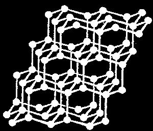
19 carbon-based materials sp 2 allotropes of carbon 2D 3D 2D OD 1D 3D Nobel lectures, Geim & Novoselov, 2010


20 carbon allotropes discovery

21 im Elektronenmikroskop Bleistift

22 im Elektronenmikroskop Bleistift

23 im Elektronenmikroskop Bleistift

24 im Elektronenmikroskop Bleistift
25 im Elektronenmikroskop Bleistift

26 im Elektronenmikroskop Bleistift

27 im Elektronenmikroskop Bleistift

28 im Elektronenmikroskop Bleistift

29 im Elektronenmikroskop Bleistift
30 im Elektronenmikroskop Bleistift

31 im Elektronenmikroskop Bleistift


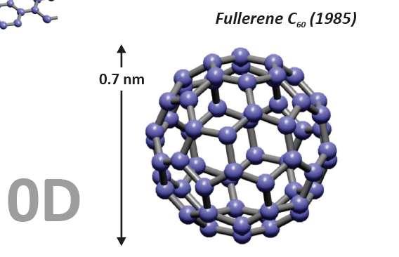
32 fullerenes fullerenes C60, C70,... Buckminster Fuller dome, Montreal, 1967 NB. 1st detection of C60, C70 in space: Cami et al., Science 2010 R.S. Smalley, Nobel lecture, 1996 Nobel.se

 in Basel for the 10 th Anniversary celebration of")
33 carbon allotropes discovery Research - PhD program Teaching bachelor & master Tech. transfer Public outreach H.G. Güntherodt ( 2014) & Harry W. Kroto ( 2016) in Basel for the 10 th Anniversary celebration of the NCCR Nanoscale Science

34 carbon allotropes discovery 2012 Kavli Prize in Nanoscience M. Dresselhaus "for her pioneering contributions to the study of phonons, electron-phonon interactions, and thermal transport in nanostructures" M.S. Dresselhaus, Cargèse, 2014


35 carbon nanotubes Single-wall or multi-wall Metallic or semiconducting Diameter: nm Length: < 100 mm S. Iijima, 1991,
 (11,0) zig-zag (n,0) or (0,n)")
=(9,9) n-m = 3*i: n-m <> 3*i: metallic")
36 carbon nanotubes structure (wrapping vector) armchair (n,n) (11,0) zig-zag (n,0) or (0,n) chiral (n,m) with n m (0,7) (11,7) armchair (n,n)=(9,9) n-m = 3*i: n-m <> 3*i: metallic semiconducting


37 carbon allotropes discovery Nobel.se


38 Graphene: scotch tape 2.0µm J. Trbovic and H. Aurich 970nm
39 graphene discovery
40 carbon-based materials and devices graphene : the missing 2D system in carbon allotropes 1947 Graphene first studied as a limiting case for theoretical work on graphite by Phillip Wallace 1966 First attempts to grow multilayer graphite Hess W M and Ban L L also Karu A E and Beer M 1984 Massless charge carriers in graphene pointed out theoretically by Gordon Walter Semenoff, David P. DeVincenzo and Eugene J. Mele 1987 Name graphene first mentioned by S. Mouras and co-workers 2004 Graphene isolated in free form by Andre Geim and Kostya Novoselov 2004 Observation of graphene s ambipolar field effect by Geim & Novoselov 2005 Anomalous quantum hall effect detected showing massless nature of charge carriers in graphene Geim, Novoselov and Kim, Zhang 2006 Quantum Hall effect seen at room temperature by Novoselov et. al first detection of a single molecule adsorption event by Schedin et. al Measurements of extremely high carrier mobility by Bolotin et. al Nobel prize in physics to Geim & Novoselov from

 correlation with distance, and hence, very large flat 2D crystalline flakes of graphene (or for that matter of any material) are manifestly allowed by this theorem.")

41 graphene: why it may have taken so long fluctuations "kill" a 2D crystal Finally, we remark on the strict 2D nature of graphene from a structural viewpoint. The existence of finite 2D flakes of graphene with crystalline order at finite temperature Landau & does Lifschitz, not instatistical any wayphysics, violate the Hohenberg-Mermin-Wagner-Coleman theorem 3 rd ed.,1980, whichpart rules I, 137 out& the 138, breaking pp of a continuous symmetry in two dimensions. This is because the theorem only asserts a slow power law decay of the crystalline (i.e., positional order) correlation with distance, and hence, very large flat 2D crystalline flakes of graphene (or for that matter of any material) are manifestly allowed by this theorem. In fact, a 2D Wigner crystal, i.e., a 2D hexagonal classical crystal of electrons in a very low-density limit, was experimentally observed more than 30 years ago (Grimes and Adams, 1979) on the surface of liquid 4He (where the electrons were bound by their image force). A simple back of the envelope calculation shows that the size of the graphene flake has to be unphysically large for this theorem to have any effect on its crystalline nature (Thompson-Flagg et al., 2009). There is nothing mysterious or remarkable about having finite 2D crystals with quasi-long-range positional order at finite temperatures, which is what we have in 2D graphene flakes. Castro-Neto et al., Rev. Mod. Phys 2011 "According to the so-called Mermin Wagner theorem 1, longwavelength fluctuations destroy the long-range order of 2D the ripples of graphene crystals. Similarly, 2D membranes embedded in a 3D space have a tendency to be crumpled 2. These fluctuations can, however, be suppressed by anharmonic coupling between bending and stretching modes meaning that a 2D membrane can exist but will exhibit strong height fluctuations." Katsnelson et al., Nature Mat. (2007)


42 graphene 0.14nm 0.12nm Mechanically strong: composite materials A 1m 2 "hamac" weighting 0.77mg could support a 4kg load nobelprize.org Flexible conductor may replace ITO High charge mobility: electrical applications


43 reminder: energy bands semimetals: small overlap between valence and conduction bands Energy gaps Si ~ 1.12 ev Ge ~ 0.66 ev GaAs ~ 1.43 ev NB: kt (RT) ~25meV
44 graphene electronic structure C: 1s 2 2s 2 2p 2 1 extra electron / p orbital half-filled p band Kane, Princeton
45 graphene electronic structure Graphene honeycomb lattice with the two triangular sublattices blue sublattice A yellow sublattice B Graphene Brillouin zone in momentum space Graphene bandstructure Valence band filled, fermi energy at E=0 for neutral graphene Zero band-gap semiconductor Two non-equivalent valleys, K and K pseudo-spin Castro Neto et al., Rev. Mod. Phys. 2009; Das Sarma et al., Rev. Mod. Phys 2011
, particles with mass: Massless particles, photons Graphene: where v F, Fermi velocity is c/300 Dirac electrons in graphene mimic the physics of quant.")
46 graphene electronic structure Low-energy excitations: massless, chiral Dirac Fermions At the Fermi energy the spectra are linear, hence the electrons are here massless. Normal materials Normal (free electrons), particles with mass: Massless particles, photons Graphene: where v F, Fermi velocity is c/300 Dirac electrons in graphene mimic the physics of quant. electrodynamics for massless Fermions Relativistic effects can be seen in graphene Castro Neto et al., Rev. Mod. Phys. 2009; Das Sarma et al., Rev. Mod. Phys 2011

47 graphene roadmap A. Ferrari, et al. 2011, 2015

48 graphene roadmap graphene-flagship.eu/

49 graphene roadmap graphene-flagship.eu/
 states: two types of edges Dresselhaus, Cargèse,")
50 adding a gap: graphene ribbons structure graphene surface (edges) states: two types of edges Dresselhaus, Cargèse, 2014


51 other 2D systems for electronics Dresselhaus, Cargèse, 2014

52 other 2D systems Transition Metal Dichalcogenides (TMDs) Chhowalla et al., Nat. Chem. (2013); Dresselhaus, Cargèse, 2014
53 other 2D systems Chhowalla et al., Nat. Chem. (2013)

54 other 2D systems Chhowalla et al., Nat. Chem. (2013)

55 other 2D systems Martel, Szkopek, Cargèse, 2014
Molecular and carbon based electronic systems
 when Wednesday, 08h15 10h00 where seminar room 3.12, Physics Dpt, Klingelbergstrasse 82 credit 2KP debit attendance + 1 presentation VV lecture Nr. 37839 01 web http://calame.unibas.ch/teaching Michel
Carbon based Nanoscale Electronics
 Carbon based Nanoscale Electronics 09 02 200802 2008 ME class Outline driving force for the carbon nanomaterial electronic properties of fullerene exploration of electronic carbon nanotube gold rush of
3-month progress Report
 3-month progress Report Graphene Devices and Circuits Supervisor Dr. P.A Childs Table of Content Abstract... 1 1. Introduction... 1 1.1 Graphene gold rush... 1 1.2 Properties of graphene... 3 1.3 Semiconductor
The many forms of carbon
 The many forms of carbon Carbon is not only the basis of life, it also provides an enormous variety of structures for nanotechnology. This versatility is connected to the ability of carbon to form two
Carbon nanomaterials. Gavin Lawes Wayne State University.
 Carbon nanomaterials Gavin Lawes Wayne State University glawes@wayne.edu Outline 1. Carbon structures 2. Carbon nanostructures 3. Potential applications for Carbon nanostructures Periodic table from bpc.edu
Graphene - most two-dimensional system imaginable
 Graphene - most two-dimensional system imaginable A suspended sheet of pure graphene a plane layer of C atoms bonded together in a honeycomb lattice is the most two-dimensional system imaginable. A.J.
Lectures Graphene and
 Lectures 15-16 Graphene and carbon nanotubes Graphene is atomically thin crystal of carbon which is stronger than steel but flexible, is transparent for light, and conducts electricity (gapless semiconductor).
Electronic properties of graphene. Jean-Noël Fuchs Laboratoire de Physique des Solides Université Paris-Sud (Orsay)
") Electronic properties of graphene Jean-Noël Fuchs Laboratoire de Physique des Solides Université Paris-Sud (Orsay) Cargèse, September 2012 3 one-hour lectures in 2 x 1,5h on electronic properties of graphene
Electronic properties of graphene Jean-Noël Fuchs Laboratoire de Physique des Solides Université Paris-Sud (Orsay) Cargèse, September 2012 3 one-hour lectures in 2 x 1,5h on electronic properties of graphene
GRAPHENE the first 2D crystal lattice
 GRAPHENE the first 2D crystal lattice dimensionality of carbon diamond, graphite GRAPHENE realized in 2004 (Novoselov, Science 306, 2004) carbon nanotubes fullerenes, buckyballs what s so special about
GRAPHENE NANORIBBONS Nahid Shayesteh,
 USC Department of Physics Graduate Seminar 1 GRAPHENE NANORIBBONS Nahid Shayesteh, Outlines 2 Carbon based material Discovery and innovation of graphen Graphene nanoribbons structure Application of Graphene
Graphite, graphene and relativistic electrons
 Graphite, graphene and relativistic electrons Introduction Physics of E. graphene Y. Andrei Experiments Rutgers University Transport electric field effect Quantum Hall Effect chiral fermions STM Dirac
Graphene and Planar Dirac Equation
 Graphene and Planar Dirac Equation Marina de la Torre Mayado 2016 Marina de la Torre Mayado Graphene and Planar Dirac Equation June 2016 1 / 48 Outline 1 Introduction 2 The Dirac Model Tight-binding model
Electronic properties of Graphene and 2-D materials
 Electronic properties of Graphene and 2-D materials 2D materials background Carbon allotropes Graphene Structure and Band structure Electronic properties Electrons in a magnetic field Onsager relation
1. Nanotechnology & nanomaterials -- Functional nanomaterials enabled by nanotechnologies.
 Novel Nano-Engineered Semiconductors for Possible Photon Sources and Detectors NAI-CHANG YEH Department of Physics, California Institute of Technology 1. Nanotechnology & nanomaterials -- Functional nanomaterials
Raman Imaging and Electronic Properties of Graphene
 Raman Imaging and Electronic Properties of Graphene F. Molitor, D. Graf, C. Stampfer, T. Ihn, and K. Ensslin Laboratory for Solid State Physics, ETH Zurich, 8093 Zurich, Switzerland ensslin@phys.ethz.ch
Black phosphorus: A new bandgap tuning knob
 Black phosphorus: A new bandgap tuning knob Rafael Roldán and Andres Castellanos-Gomez Modern electronics rely on devices whose functionality can be adjusted by the end-user with an external knob. A new
ELECTRONIC ENERGY DISPERSION AND STRUCTURAL PROPERTIES ON GRAPHENE AND CARBON NANOTUBES
 ELECTRONIC ENERGY DISPERSION AND STRUCTURAL PROPERTIES ON GRAPHENE AND CARBON NANOTUBES D. RACOLTA, C. ANDRONACHE, D. TODORAN, R. TODORAN Technical University of Cluj Napoca, North University Center of
Graphene. Tianyu Ye November 30th, 2011
 Graphene Tianyu Ye November 30th, 2011 Outline What is graphene? How to make graphene? (Exfoliation, Epitaxial, CVD) Is it graphene? (Identification methods) Transport properties; Other properties; Applications;
Graphene and Carbon Nanotubes
 Graphene and Carbon Nanotubes 1 atom thick films of graphite atomic chicken wire Novoselov et al - Science 306, 666 (004) 100μm Geim s group at Manchester Novoselov et al - Nature 438, 197 (005) Kim-Stormer
Classification of Solids
 Classification of Solids Classification by conductivity, which is related to the band structure: (Filled bands are shown dark; D(E) = Density of states) Class Electron Density Density of States D(E) Examples
Supplementary Figure 2 Photoluminescence in 1L- (black line) and 7L-MoS 2 (red line) of the Figure 1B with illuminated wavelength of 543 nm.
 and 7L-MoS 2 (red line) of the Figure 1B with illuminated wavelength of 543 nm.") PL (normalized) Intensity (arb. u.) 1 1 8 7L-MoS 1L-MoS 6 4 37 38 39 4 41 4 Raman shift (cm -1 ) Supplementary Figure 1 Raman spectra of the Figure 1B at the 1L-MoS area (black line) and 7L-MoS area (red
PL (normalized) Intensity (arb. u.) 1 1 8 7L-MoS 1L-MoS 6 4 37 38 39 4 41 4 Raman shift (cm -1 ) Supplementary Figure 1 Raman spectra of the Figure 1B at the 1L-MoS area (black line) and 7L-MoS area (red
PHYS-E0424 Nanophysics Lecture 5: Fullerenes, Carbon Nanotubes and Graphene
 PHYS-E0424 Nanophysics Lecture 5: Fullerenes, Carbon Nanotubes and Graphene PHYS-E0424 Nanophysics Lecture 5: Carbon Nanostructures Sebastiaan van Dijken 1 SEM/TEM Recently I was operating SEM for a first
Graphene transistor. Seminar I a. Mentor: doc. dr. Tomaž Rejec. April Abstract
 Graphene transistor Seminar I a Jan Srpčič Mentor: doc. dr. Tomaž Rejec April 2015 Abstract The topic of this seminar is graphene and its possible applications in the field of electronics, most notably
The Photophysics of Nano Carbons. Kavli Institute, UC Santa Barbara January 9, 2012 M. S. Dresselhaus, MIT
 The Photophysics of Nano Carbons Kavli Institute, UC Santa Barbara January 9, 2012 M. S. Dresselhaus, MIT The Electronic Structure of Graphene Near the K point E ( ) v F linear relation where and and 0
2D Materials with Strong Spin-orbit Coupling: Topological and Electronic Transport Properties
 2D Materials with Strong Spin-orbit Coupling: Topological and Electronic Transport Properties Artem Pulkin California Institute of Technology (Caltech), Pasadena, CA 91125, US Institute of Physics, Ecole
per unit cell Motif: Re at (0, 0, 0); 3O at ( 1 / 2, 0), (0, 0, 1 / 2 ) Re: 6 (octahedral coordination) O: 2 (linear coordination) ReO 6
; 3O at ( 1 / 2, 0), (0, 0, 1 / 2 ) Re: 6 (octahedral coordination) O: 2 (linear coordination) ReO 6") Lattice: Primitive Cubic 1ReO 3 per unit cell Motif: Re at (0, 0, 0); 3O at ( 1 / 2, 0, 0), (0, 1 / 2, 0), (0, 0, 1 / 2 ) Re: 6 (octahedral coordination) O: 2 (linear coordination) ReO 6 octahedra share
Lattice: Primitive Cubic 1ReO 3 per unit cell Motif: Re at (0, 0, 0); 3O at ( 1 / 2, 0, 0), (0, 1 / 2, 0), (0, 0, 1 / 2 ) Re: 6 (octahedral coordination) O: 2 (linear coordination) ReO 6 octahedra share
Graphene The Search For Two Dimensions. Christopher Scott Friedline Arizona State University
 Graphene The Search For Two Dimensions Christopher Scott Friedline Arizona State University What Is Graphene? Single atomic layer of graphite arranged in a honeycomb crystal lattice Consists of sp 2 -bonded
Physics of Nanotubes, Graphite and Graphene Mildred Dresselhaus
 Quantum Transport and Dynamics in Nanostructures The 4 th Windsor Summer School on Condensed Matter Theory 6-18 August 2007, Great Park Windsor (UK) Physics of Nanotubes, Graphite and Graphene Mildred
Nanoscience quantum transport
 Nanoscience quantum transport Janine Splettstößer Applied Quantum Physics, MC2, Chalmers University of Technology Chalmers, November 2 10 Plan/Outline 4 Lectures (1) Introduction to quantum transport (2)
Carbon nanotubes and Graphene
 16 October, 2008 Solid State Physics Seminar Main points 1 History and discovery of Graphene and Carbon nanotubes 2 Tight-binding approximation Dynamics of electrons near the Dirac-points 3 Properties
Lecture Quantum Information Processing II: Implementations. spring term (FS) 2017
 2017") Lecture Quantum Information Processing II: Implementations spring term (FS) 2017 Lectures & Exercises: Andreas Wallraff, Christian Kraglund Andersen, Christopher Eichler, Sebastian Krinner Please take
Lecture Quantum Information Processing II: Implementations spring term (FS) 2017 Lectures & Exercises: Andreas Wallraff, Christian Kraglund Andersen, Christopher Eichler, Sebastian Krinner Please take
EE236 Electronics. Computer and Systems Engineering Department. Faculty of Engineering Alexandria University. Fall 2014
 EE236 Electronics Computer and Systems Engineering Department Faculty of Engineering Alexandria University Fall 2014 Lecturer: Bassem Mokhtar, Ph.D. Assistant Professor Department of Electrical Engineering
Overview. Carbon in all its forms. Background & Discovery Fabrication. Important properties. Summary & References. Overview of current research
 Graphene Prepared for Solid State Physics II Pr Dagotto Spring 2009 Laurene Tetard 03/23/09 Overview Carbon in all its forms Background & Discovery Fabrication Important properties Overview of current
Graphene: the Route from Touch Screens to Digital Nanoelectronics
 Graphene: the Route from Touch Screens to Digital Nanoelectronics László Péter Biró Research Institute for Technical Physics & Materials Science, Budapest, Hungary http://www.nanotechnology.hu/ Human History
Charge-Carrier Transport in Graphene
 Charge-Carrier Transport in Graphene P.V. Buividovich, O.V. Pavlovsky, M.V. Ulybyshev, E.V. Luschevskaya, M.A. Zubkov, V.V. Braguta, M.I. Polikarpov ArXiv:1204.0921; ArXiv:1206.0619 Introduction: QCD and
Graphene: fundamentals
 Graphene: fundamentals François Peeters Condensed Matter Theory group Department of Physics University of Antwerp Email: francois.peeters@uantwerpen.be https://www.uantwerpen.be/en/rg/cmt/ Chemistry Graphitic
CHAPTER 11 Semiconductor Theory and Devices
 CHAPTER 11 Semiconductor Theory and Devices 11.1 Band Theory of Solids 11.2 Semiconductor Theory 11.3 Semiconductor Devices 11.4 Nanotechnology It is evident that many years of research by a great many
2D MBE Activities in Sheffield. I. Farrer, J. Heffernan Electronic and Electrical Engineering The University of Sheffield
 2D MBE Activities in Sheffield I. Farrer, J. Heffernan Electronic and Electrical Engineering The University of Sheffield Outline Motivation Van der Waals crystals The Transition Metal Di-Chalcogenides
2-D Layered Materials 1
 2-D Layered Materials 1 Flatlands beyond Graphene Why the interest? 2D crystal with extraordinarily few defects Exotic electrical behaviors E = v F P (massless Dirac fermions) Efficient tunneling through
Electronics with 2D Crystals: Scaling extender, or harbinger of new functions?
 Electronics with 2D Crystals: Scaling extender, or harbinger of new functions? 1 st Workshop on Data Abundant Systems Technology Stanford, April 2014 Debdeep Jena (djena@nd.edu) Electrical Engineering,
Nanostructures. Lecture 13 OUTLINE
 Nanostructures MTX9100 Nanomaterials Lecture 13 OUTLINE -What is quantum confinement? - How can zero-dimensional materials be used? -What are one dimensional structures? -Why does graphene attract so much
Halbleiter Prof. Yong Lei Prof. Thomas Hannappel
 Halbleiter Prof. Yong Lei Prof. Thomas Hannappel yong.lei@tu-ilmenau.de thomas.hannappel@tu-ilmenau.de http:///nanostruk/ Organic semiconductors Small-molecular materials Rubrene Pentacene Polymers PEDOT:PSS
Initial Stages of Growth of Organic Semiconductors on Graphene
 Initial Stages of Growth of Organic Semiconductors on Graphene Presented by: Manisha Chhikara Supervisor: Prof. Dr. Gvido Bratina University of Nova Gorica Outline Introduction to Graphene Fabrication
EE130: Integrated Circuit Devices
 EE130: Integrated Circuit Devices (online at http://webcast.berkeley.edu) Instructor: Prof. Tsu-Jae King (tking@eecs.berkeley.edu) TA s: Marie Eyoum (meyoum@eecs.berkeley.edu) Alvaro Padilla (apadilla@eecs.berkeley.edu)
Graphene and Quantum Hall (2+1)D Physics
D Physics") The 4 th QMMRC-IPCMS Winter School 8 Feb 2011, ECC, Seoul, Korea Outline 2 Graphene and Quantum Hall (2+1)D Physics Lecture 1. Electronic structures of graphene and bilayer graphene Lecture 2. Electrons
The 4 th QMMRC-IPCMS Winter School 8 Feb 2011, ECC, Seoul, Korea Outline 2 Graphene and Quantum Hall (2+1)D Physics Lecture 1. Electronic structures of graphene and bilayer graphene Lecture 2. Electrons
Wafer-scale fabrication of graphene
 Wafer-scale fabrication of graphene Sten Vollebregt, MSc Delft University of Technology, Delft Institute of Mircosystems and Nanotechnology Delft University of Technology Challenge the future Delft University
Molecular Dynamics Study of Thermal Rectification in Graphene Nanoribbons
 Molecular Dynamics Study of Thermal Rectification in Graphene Nanoribbons Jiuning Hu 1* Xiulin Ruan 2 Yong P. Chen 3# 1School of Electrical and Computer Engineering and Birck Nanotechnology Center, Purdue
From nanophysics research labs to cell phones. Dr. András Halbritter Department of Physics associate professor
 From nanophysics research labs to cell phones Dr. András Halbritter Department of Physics associate professor Curriculum Vitae Birth: 1976. High-school graduation: 1994. Master degree: 1999. PhD: 2003.
Fermi polaron-polaritons in MoSe 2
 Fermi polaron-polaritons in MoSe 2 Meinrad Sidler, Patrick Back, Ovidiu Cotlet, Ajit Srivastava, Thomas Fink, Martin Kroner, Eugene Demler, Atac Imamoglu Quantum impurity problem Nonperturbative interaction
Graphene Novel Material for Nanoelectronics
 Graphene Novel Material for Nanoelectronics Shintaro Sato Naoki Harada Daiyu Kondo Mari Ohfuchi (Manuscript received May 12, 2009) Graphene is a flat monolayer of carbon atoms with a two-dimensional honeycomb
Nanostrukturphysik (Nanostructure Physics)
") Nanostrukturphysik (Nanostructure Physics) Prof. Yong Lei & Dr. Yang Xu Fachgebiet 3D-Nanostrukturierung, Institut für Physik Contact: yong.lei@tu-ilmenau.de; yang.xu@tu-ilmenau.de Office: Unterpoerlitzer
Nanostrukturphysik (Nanostructure Physics) Prof. Yong Lei & Dr. Yang Xu Fachgebiet 3D-Nanostrukturierung, Institut für Physik Contact: yong.lei@tu-ilmenau.de; yang.xu@tu-ilmenau.de Office: Unterpoerlitzer
Quantum transport through graphene nanostructures
 Quantum transport through graphene nanostructures S. Rotter, F. Libisch, L. Wirtz, C. Stampfer, F. Aigner, I. Březinová, and J. Burgdörfer Institute for Theoretical Physics/E136 December 9, 2009 Graphene
TRANSVERSE SPIN TRANSPORT IN GRAPHENE
 International Journal of Modern Physics B Vol. 23, Nos. 12 & 13 (2009) 2641 2646 World Scientific Publishing Company TRANSVERSE SPIN TRANSPORT IN GRAPHENE TARIQ M. G. MOHIUDDIN, A. A. ZHUKOV, D. C. ELIAS,
Nanotechnology in Consumer Products
 Nanotechnology in Consumer Products June 17, 2015 October 31, 2014 The webinar will begin at 1pm Eastern Time Perform an audio check by going to Tools > Audio > Audio Setup Wizard Chat Box Chat Box Send
EN2912C: Future Directions in Computing Lecture 08: Overview of Near-Term Emerging Computing Technologies
 EN2912C: Future Directions in Computing Lecture 08: Overview of Near-Term Emerging Computing Technologies Prof. Sherief Reda Division of Engineering Brown University Fall 2008 1 Near-term emerging computing
Graphene: massless electrons in flatland.
 Graphene: massless electrons in flatland. Enrico Rossi Work supported by: University of Chile. Oct. 24th 2008 Collaorators CMTC, University of Maryland Sankar Das Sarma Shaffique Adam Euyuong Hwang Roman
Graphene. L. Tetard 1,2. (Dated: April 7, 2009) 1 Oak Ridge National Laboratory, Oak Ridge, TN USA
 1 Oak Ridge National Laboratory, Oak Ridge, TN USA") Graphene L. Tetard 1,2 1 Oak Ridge National Laboratory, Oak Ridge, TN 37831-6123 USA 2 Department of Physics, University of Tennessee, Knoxville, TN 37996, USA (Dated: April 7, 2009) 1 Diamond, graphite,
Graphene L. Tetard 1,2 1 Oak Ridge National Laboratory, Oak Ridge, TN 37831-6123 USA 2 Department of Physics, University of Tennessee, Knoxville, TN 37996, USA (Dated: April 7, 2009) 1 Diamond, graphite,
Supporting Information. by Hexagonal Boron Nitride
 Supporting Information High Velocity Saturation in Graphene Encapsulated by Hexagonal Boron Nitride Megan A. Yamoah 1,2,, Wenmin Yang 1,3, Eric Pop 4,5,6, David Goldhaber-Gordon 1 * 1 Department of Physics,
Electron Interactions and Nanotube Fluorescence Spectroscopy C.L. Kane & E.J. Mele
 Electron Interactions and Nanotube Fluorescence Spectroscopy C.L. Kane & E.J. Mele Large radius theory of optical transitions in semiconducting nanotubes derived from low energy theory of graphene Phys.
PHYS 3313 Section 001 Lecture #21 Monday, Nov. 26, 2012
 PHYS 3313 Section 001 Lecture #21 Monday, Nov. 26, 2012 Superconductivity Theory, The Cooper Pair Application of Superconductivity Semi-Conductor Nano-technology Graphene 1 Announcements Your presentations
PH575 Spring Lecture #28 Nanoscience: the case study of graphene and carbon nanotubes.
 PH575 Spring 2014 Lecture #28 Nanoscience: the case study of graphene and carbon nanotubes. Nanoscience scale 1-100 nm "Artificial atoms" Small size => discrete states Large surface to volume ratio Bottom-up
Molecular Dynamics Study of Thermal Rectification in Graphene Nanoribbons
 Int J Thermophys (2012) 33:986 991 DOI 10.1007/s10765-012-1216-y Molecular Dynamics Study of Thermal Rectification in Graphene Nanoribbons Jiuning Hu Xiulin Ruan Yong P. Chen Received: 26 June 2009 / Accepted:
Physical Properties of Mono-layer of
 Chapter 3 Physical Properties of Mono-layer of Silicene The fascinating physical properties[ 6] associated with graphene have motivated many researchers to search for new graphene-like two-dimensional
GRAPHENE NANORIBBONS Nahid Shayesteh,
 USC Department of Physics Graduate Seminar GRAPHENE NANORIBBONS Nahid Shayesteh, Outlines 2 Carbon based material Discovery and innovation of graphen Graphene nanoribbons structure and... FUNCTIONS 3 Carbon-based
STM and graphene. W. W. Larry Pai ( 白偉武 ) Center for condensed matter sciences, National Taiwan University NTHU, 2013/05/23
 Center for condensed matter sciences, National Taiwan University NTHU, 2013/05/23") STM and graphene W. W. Larry Pai ( 白偉武 ) Center for condensed matter sciences, National Taiwan University NTHU, 2013/05/23 Why graphene is important: It is a new form of material (two dimensional, single
STM and graphene W. W. Larry Pai ( 白偉武 ) Center for condensed matter sciences, National Taiwan University NTHU, 2013/05/23 Why graphene is important: It is a new form of material (two dimensional, single
CMOS Scaling. Two motivations to scale down. Faster transistors, both digital and analog. To pack more functionality per area. Lower the cost!
 Two motivations to scale down CMOS Scaling Faster transistors, both digital and analog To pack more functionality per area. Lower the cost! (which makes (some) physical sense) Scale all dimensions and
Transversal electric field effect in multilayer graphene nanoribbon
 Transversal electric field effect in multilayer graphene nanoribbon S. Bala kumar and Jing Guo a) Department of Electrical and Computer Engineering, University of Florida, Gainesville, Florida 32608, USA
Conference Return Seminar- NANO2014,Moscow State University,Moscow,Russia Date: th July 2014
 Conference Return Seminar- NANO2014,Moscow State University,Moscow,Russia Date:13-1818 th July 2014 An electrochemical method for the synthesis of single and few layers graphene sheets for high temperature
Surfaces, Interfaces, and Layered Devices
 Surfaces, Interfaces, and Layered Devices Building blocks for nanodevices! W. Pauli: God made solids, but surfaces were the work of Devil. Surfaces and Interfaces 1 Interface between a crystal and vacuum
Carbon Nanomaterials
 Carbon Nanomaterials STM Image 7 nm AFM Image Fullerenes C 60 was established by mass spectrographic analysis by Kroto and Smalley in 1985 C 60 is called a buckminsterfullerene or buckyball due to resemblance
Introduction to Nanotechnology Chapter 5 Carbon Nanostructures Lecture 1
 Introduction to Nanotechnology Chapter 5 Carbon Nanostructures Lecture 1 ChiiDong Chen Institute of Physics, Academia Sinica chiidong@phys.sinica.edu.tw 02 27896766 Section 5.2.1 Nature of the Carbon Bond
REVIEW Antonio H. Castro Neto Human progress and development has always been marked by
 The carbon new age Graphene has been considered by many as a revolutionary material with electronic and structural properties that surpass conventional semiconductors and metals. Due to its superlative
Minimal Update of Solid State Physics
 Minimal Update of Solid State Physics It is expected that participants are acquainted with basics of solid state physics. Therefore here we will refresh only those aspects, which are absolutely necessary
From graphene to Z2 topological insulator
 From graphene to Z2 topological insulator single Dirac topological AL mass U U valley WL ordinary mass or ripples WL U WL AL AL U AL WL Rashba Ken-Ichiro Imura Condensed-Matter Theory / Tohoku Univ. Dirac
From Last Time. Several important conceptual aspects of quantum mechanics Indistinguishability. Symmetry
 From Last Time Several important conceptual aspects of quantum mechanics Indistinguishability particles are absolutely identical Leads to Pauli exclusion principle (one Fermion / quantum state). Symmetry
Why are we so excited about carbon nanostructures? Mildred Dresselhaus Massachusetts Institute of Technology Cambridge, MA
 Why are we so excited about carbon nanostructures? Mildred Dresselhaus Massachusetts Institute of Technology Cambridge, MA Conference for Undergraduate Women in Physics at Yale January 18, 2009 Why are
Transient Photocurrent Measurements of Graphene Related Materials
 Transient Photocurrent Measurements of Graphene Related Materials P. Srinivasa Rao Mentor: Prof. dr. Gvido Bratina Laboratory of Organic Matter Physics University of Nova Gorica 1 Contents: 1. Electrical
Seminars in Nanosystems - I
 Seminars in Nanosystems - I Winter Semester 2011/2012 Dr. Emanuela Margapoti Emanuela.Margapoti@wsi.tum.de Dr. Gregor Koblmüller Gregor.Koblmueller@wsi.tum.de Seminar Room at ZNN 1 floor Topics of the
Scanning tunneling microscopy and spectroscopy of graphene layers on graphite
 Scanning tunneling microscopy and spectroscopy of graphene layers on graphite Adina Luican, Guohong Li and Eva Y. Andrei Department of Physics and Astronomy, Rutgers University, Piscataway, New Jersey
Nanoscience, MCC026 2nd quarter, fall Quantum Transport, Lecture 1/2. Tomas Löfwander Applied Quantum Physics Lab
 Nanoscience, MCC026 2nd quarter, fall 2012 Quantum Transport, Lecture 1/2 Tomas Löfwander Applied Quantum Physics Lab Quantum Transport Nanoscience: Quantum transport: control and making of useful things
Recap (so far) Low-Dimensional & Boundary Effects
 Low-Dimensional & Boundary Effects") Recap (so far) Ohm s & Fourier s Laws Mobility & Thermal Conductivity Heat Capacity Wiedemann-Franz Relationship Size Effects and Breakdown of Classical Laws 1 Low-Dimensional & Boundary Effects Energy
Recap (so far) Ohm s & Fourier s Laws Mobility & Thermal Conductivity Heat Capacity Wiedemann-Franz Relationship Size Effects and Breakdown of Classical Laws 1 Low-Dimensional & Boundary Effects Energy
Metals: the Drude and Sommerfeld models p. 1 Introduction p. 1 What do we know about metals? p. 1 The Drude model p. 2 Assumptions p.
 Metals: the Drude and Sommerfeld models p. 1 Introduction p. 1 What do we know about metals? p. 1 The Drude model p. 2 Assumptions p. 2 The relaxation-time approximation p. 3 The failure of the Drude model
Carbon Nanotubes (CNTs)
") Carbon Nanotubes (s) Seminar: Quantendynamik in mesoskopischen Systemen Florian Figge Fakultät für Physik Albert-Ludwigs-Universität Freiburg July 7th, 2010 F. Figge (University of Freiburg) Carbon Nanotubes
Carbon Nanotubes (s) Seminar: Quantendynamik in mesoskopischen Systemen Florian Figge Fakultät für Physik Albert-Ludwigs-Universität Freiburg July 7th, 2010 F. Figge (University of Freiburg) Carbon Nanotubes
News from NBIA. Condensed Matter Physics: from new materials to quantum technology. time. Mark Rudner
 News from NBIA Condensed Matter Physics: from new materials to quantum technology Mark Rudner time ~100 years after Bohr, the basic laws and players are established 1913 2013 Image from www.periodni.com
Supplementary Figure S1. AFM images of GraNRs grown with standard growth process. Each of these pictures show GraNRs prepared independently,
 Supplementary Figure S1. AFM images of GraNRs grown with standard growth process. Each of these pictures show GraNRs prepared independently, suggesting that the results is reproducible. Supplementary Figure
Calculating Electronic Structure of Different Carbon Nanotubes and its Affect on Band Gap
 Calculating Electronic Structure of Different Carbon Nanotubes and its Affect on Band Gap 1 Rashid Nizam, 2 S. Mahdi A. Rizvi, 3 Ameer Azam 1 Centre of Excellence in Material Science, Applied Physics AMU,
EE143 Fall 2016 Microfabrication Technologies. Evolution of Devices
 EE143 Fall 2016 Microfabrication Technologies Prof. Ming C. Wu wu@eecs.berkeley.edu 511 Sutardja Dai Hall (SDH) 1-1 Evolution of Devices Yesterday s Transistor (1947) Today s Transistor (2006) 1-2 1 Why
Conductance of Graphene Nanoribbon Junctions and the Tight Binding Model
 Wu and Childs Nanoscale es Lett, 6:6 http://www.nanoscalereslett.com/content/6//6 NANO EXPE Open Access Conductance of Graphene Nanoribbon Junctions and the Tight Binding Model Y Wu, PA Childs * Abstract
Dirac matter: Magneto-optical studies
 Dirac matter: Magneto-optical studies Marek Potemski Laboratoire National des Champs Magnétiques Intenses Grenoble High Magnetic Field Laboratory CNRS/UGA/UPS/INSA/EMFL MOMB nd International Conference
Semiconductors and Optoelectronics. Today Semiconductors Acoustics. Tomorrow Come to CH325 Exercises Tours
 Semiconductors and Optoelectronics Advanced Physics Lab, PHYS 3600 Don Heiman, Northeastern University, 2017 Today Semiconductors Acoustics Tomorrow Come to CH325 Exercises Tours Semiconductors and Optoelectronics
Graphene based FETs. Raghav Gupta ( )
") 1 Graphene based FETs Raghav Gupta (10327553) Abstract The extraordinary electronic properties along with excellent optical, mechanical, thermodynamic properties have led to a lot of interest in its possible
1 Graphene based FETs Raghav Gupta (10327553) Abstract The extraordinary electronic properties along with excellent optical, mechanical, thermodynamic properties have led to a lot of interest in its possible
From graphene to graphite: Electronic structure around the K point
 PHYSICL REVIEW 74, 075404 2006 From graphene to graphite: Electronic structure around the K point. Partoens* and F. M. Peeters Universiteit ntwerpen, Departement Fysica, Groenenborgerlaan 171, -2020 ntwerpen,
SCIENCE & TECHNOLOGY
 Pertanika J. Sci. & Technol. 25 (S): 205-212 (2017) SCIENCE & TECHNOLOGY Journal homepage: http://www.pertanika.upm.edu.my/ Effect of Boron and Oxygen Doping to Graphene Band Structure Siti Fazlina bt
Modern Physics for Scientists and Engineers International Edition, 4th Edition
 Modern Physics for Scientists and Engineers International Edition, 4th Edition http://optics.hanyang.ac.kr/~shsong 1. THE BIRTH OF MODERN PHYSICS 2. SPECIAL THEORY OF RELATIVITY 3. THE EXPERIMENTAL BASIS
A comparative computational study of the electronic properties of planar and buckled silicene
 A comparative computational study of the electronic properties of planar and buckled silicene Harihar Behera 1 and Gautam Mukhopadhyay 2 Indian Institute of Technology Bombay, Powai, Mumbai-400076, India
3C3 Analogue Circuits
 Department of Electronic & Electrical Engineering Trinity College Dublin, 2014 3C3 Analogue Circuits Prof J K Vij jvij@tcd.ie Lecture 1: Introduction/ Semiconductors & Doping 1 Course Outline (subject
Carbon Nanomaterials: Nanotubes and Nanobuds and Graphene towards new products 2030
 Carbon Nanomaterials: Nanotubes and Nanobuds and Graphene towards new products 2030 Prof. Dr. Esko I. Kauppinen Helsinki University of Technology (TKK) Espoo, Finland Forecast Seminar February 13, 2009
Graphene, the two-dimensional allotrope of carbon,
 External Bias Dependent Direct To Indirect Band Gap Transition in Graphene Nanoribbon Kausik Majumdar,*, Kota V. R. M. Murali, Navakanta Bhat, and Yu-Ming Lin pubs.acs.org/nanolett Department of Electrical
ET3034TUx Utilization of band gap energy
 ET3034TUx - 3.3.1 - Utilization of band gap energy In the last two weeks we have discussed the working principle of a solar cell and the external parameters that define the performance of a solar cell.
Projected Performance Advantage of Multilayer Graphene Nanoribbon as Transistor Channel Material
 Projected Performance Advantage of Multilayer Graphene Nanoribbon as Transistor Channel Material Yijian Ouyang 1, Hongjie Dai 2, and Jing Guo 1 1 Department of Electrical and Computer Engineering, University