Lecture 4. Conductance sensors. ChemFET. Electrochemical Impedance Spectroscopy. py Practical consideration for electrochemical biosensors.
|
|
|
- Brent Snow
- 5 years ago
- Views:
Transcription
1 Lecture 4 Conductance sensors. ChemFET. Electrochemical Impedance Spectroscopy. py Practical consideration for electrochemical biosensors.
2 Conductivity I V = I R=, L - conductance L= κa/, l Λ= κ /[ C] L Directly proportional to the concentration of ions in the solution Depends on charge, mobility and degree of dissocation of ions Any reaction that produces change in a number of ions or in the charge of ions can be monitored. No selectivity in itself
3 Electrode: solid metal f Fermi distribution only electrones within kt of Ef can be transferred = 1/(1 + exp( E E ) / kt) F High electron density Additional effect related to crystallographic orientation, reorganisation of metal surface during potential ti cycling etc.
4 Semiconductor electrode (intrinsic semiconductor) Band gap E f in the middle of the gap Number of excited electrons ~exp(- E g /2kT) Lower density of state, space-charge region is large and therefore most of potential variation occurs there (Cd~10-100uF, Csc<1uF)
5
6 Doped semiconductors N-type P-type
7 Types of space charge region in n-type semiconductor Flat-band potential Accumulation layer Depletion layer Inversion
8 Semiconductor-solution contact semiconductor and liquid id separated: equilibrium in the dark: Fermi level is aligned to E 0. photocatalysis
9 ChemFET: Chemically sensitive FET
10 ChemFET: Chemically sensitive FET ChemFET Ion-selective membrane: ISFET Enzyme membrane: EnFET Membranes with mobile ionexchanger Membranes containing neutral ionophores Membranes with fixed ionic sites based on interaction of enzyme with analyte, extremely selective
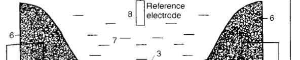
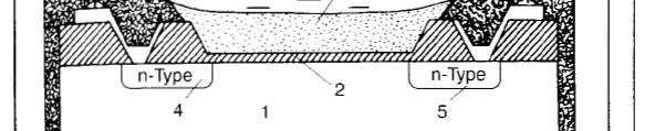
11 The image cannot be displayed. Your computer may not have enough memory to open the image, or the image may have been corrupted. Restart your computer, and then open the file again. If the red x still appears, you may have to delete the image and then insert it again. The image cannot be displayed. Your computer may not have enough memory to open the image, or the image may have been corrupted. Restart your computer, and then open the file again. If the red x still appears, you may have to delete the image and then insert it again. ChemFET fabrication Gate Material Source Contact Drain Contact (Ti, Au) (Ti, Au) PECVD SiO 2 SiO 2 Source n-silicon Gate Insulator (SiO 2, Si 3 N 4 ) Substrate p-silicon Drain n-silicon Backside Contact (Ti, Au)


12 The image cannot be displayed. Your computer may not have enough memory to open the image, or the image may have been corrupted. Restart your computer, and then open the file again. If the red x still appears, you may have to delete the image and then insert it again. Process Snapshots Source Gate Drain Working Area Lithography Conducting Polymer Deposition Epoxy Well Definition Wire bonded to Header
13 Impedance spectroscopy Reactions on the surface (e.g. formation of a recognition complex) will lead to change of capacitance and resistance of electrode-solution interface Impedance is a complex resistance encountered when current flows through h a circuit it containing i resistors, capacitors and inductors Randles and Ersher equivalent circuit model C dl double layer capacitance R et electron transfer resistance R s Ohmic resistance of the solution Z w Warburg impedance due to diffusion of ions from bulk to the surface
14 Impedance spectroscopy From the circuit theory: impedance of basic electric elements: So, we can calculate the So, we can calculate the impedance of our circuit
15 Impedance spectroscopy The impedance can written as: 2 R R C et et d Z ( ω ) = R + = s jω Z jz ω R C 1+ ω R C + et d et d semi-circle: electron transport t controlled linear part: due to diffusion-controlled impedance ω = R et 0 1 C R dl et Typical frequency range: 10mHz 100 khz (limited by the wires and e/chem cell)
16 Impedance spectroscopy Depend on dielectric and conductive properties of the interface = + C C C dl bare mod R = R + R et bare mod Represent bulk properties of the solution, not affected by the reactions at the interface
17 Immunosensors based on impedance spectroscopy In-plane impedance measurements Affinity binding in the gap results in the change of the electrical properties affecting the impedance between the electrodes: main contribution: capacitive changes due to change in dielectric constant Variations: labelling IgG with bubble generating enzyme (e.g. catalase) to increase the change in dielectric constant labelling IgG with conductive polymer chains discontinuous metallic film in the gap
18 Immunosensors based on impedance spectroscopy Examples Increase in conductivity upon binding of polyaniline labelled IgG Increase in conductivity of copper phtalocyanine upon I 2 doping
19 Immunosensors based on impedance spectroscopy Interfacial impedance measurements Formation of antigenantibody complex results in: increase of the double-layer thickness insulation of the electrode surface in respect to redox couple added to the solution
20 Immunosensors based on impedance spectroscopy Example: sensor for foot-and-mouth disease using faradeic spectroscopy (with 2mM Fe(CN) 6 ) -3/-4 ) bare gold electrode functionalized gold electrode upon binding of antigen
21 Practical considerations

22 Electrochemical cell for voltammetry gas purging: oxygen removal is essential for many experiments as oxygen and its products can affect the process in question O + 2H + 2 e H O -0.1V vs SCE HO + 2H + 2e 2 HO -0.9V vs SCE temperature controlled environment Faraday cage magnetic stirrer


23 Instrumentation Fully automated system for voltammetry measurements Research grade system with capability for multiple techniques
24 Working electrodes Dropping mercury electrode (DME)

, extreme hardness metal electrodes: good electron transfer")
25 Solid electrodes: Working electrodes stationary y( (usually cylindrical rod in an insulating sleeve) rotating Material for solid electrodes: carbon glassy carbon: wide potential window, chemically inert, can be made porous carbon paste electrode: graphite powder+ organic binder diamond electrodes (boron-doped): low double layer capacitance (due to absence of C-O bonds), extreme hardness metal electrodes: good electron transfer kinteics
26 Working electrodes Material for solid electrodes: metal electrodes made of noble metals: good electron transfer kinetics large anodic window small cathodic window due to low hydrogen overvoltage ( V depending on ph) high background currents associate with formation of surface oxide and hydrogen layers other metals can be used depending on application (Cu, Ni, Ag, Pt-Ru etc.) Pt oxide formation and reduction in 0.5M H 2 SO 4.
27 Working electrodes Chemically modified electrodes: properties of electrode are deliberately changed by placement of a reagent onto the surface self assembled monolayers RSH + Au RS Au + e + H + CNT modified electrodes Sol-gel encapsulation of reactive species (3D hydroxilated network is formed for entrapment of a modifier) Electrocatalytically modified electrodes (with mediator, e.g. NADH, Co-phtalocyanine etc.) Pre-concentrating electrodes
28 Working electrodes Chemically modified electrodes: CNT modified electrodes Sol-gel encapsulation of reactive species (3D hydroxilated network is formed for entrapment of a modifier) Electrocatalytically modified electrodes (with mediator, e.g. NADH, Co-phtalocyanine etc.) Pre-concentrating electrodes: collecting analyte via nonelectrolytic step Permselectrive coating: improving selective by allowing transport of analyte while excluding the unwanted species
29 Working electrodes Chemically modified electrodes: Permselectrive coating: improving selective by allowing transport of analyte while excluding the unwanted species, e.g. via size exclusion via charge exclusion Conducting polymer possibility to switch between conducting and insulating form polymer nanowires molecular imprinted polymers via electropolymerization Nafion-coated electrode: excluding anionic interference due to negatively charged sulfonated groups in the pores
30 Microelectrodes Working electrodes measurement of in microflow systems, analysis of small samples in vivo measurements possibility to work in highly resistive solutions reduced double layer capacitance large component of spherical diffusion
Current based methods
 Current based methods Amperometric and voltammetric sensors More significant influence on analytical parameters (sensitivity, selectivity, interferences elimination) kind of method, potential range, electrode
VI. EIS STUDIES LEAD NANOPOWDER
 VI. EIS STUDIES LEAD NANOPOWDER 74 26. EIS Studies of Pb nanospheres Impedance (valid for both DC and AC), a complex resistance occurs when current flows through a circuit (composed of various resistors,
SUPPLEMENTARY INFORMATION
 doi:10.1038/nature17653 Supplementary Methods Electronic transport mechanism in H-SNO In pristine RNO, pronounced electron-phonon interaction results in polaron formation that dominates the electronic
e - Galvanic Cell 1. Voltage Sources 1.1 Polymer Electrolyte Membrane (PEM) Fuel Cell
 Fuel Cell") Galvanic cells convert different forms of energy (chemical fuel, sunlight, mechanical pressure, etc.) into electrical energy and heat. In this lecture, we are interested in some examples of galvanic cells.
Galvanic cells convert different forms of energy (chemical fuel, sunlight, mechanical pressure, etc.) into electrical energy and heat. In this lecture, we are interested in some examples of galvanic cells.
During such a time interval, the MOS is said to be in "deep depletion" and the only charge present in the semiconductor is the depletion charge.
 Q1 (a) If we apply a positive (negative) voltage step to a p-type (n-type) MOS capacitor, which is sufficient to generate an inversion layer at equilibrium, there is a time interval, after the step, when
Chemical and Biochemical Microsystems
 Chemical and Biochemical Microsystems 1. Chemical Sensors 2. Chemical Actuators 3. Bioelectric Devices 4. Example: Electronic Nose (C) Andrei Sazonov 2005, 2006 1 Generally, chemical microsystems are used
Chapter 25. Voltammetry
 Chapter 5. Voltammetry Excitation Signal in Voltammetry Voltammetric Instrumentation Hydrodynamic Voltammetry Cyclic Voltammetry Pulse Voltammetry High-Frequency and High-Speed Voltammetry Application
The interfacial study on the Cu 2 O/Ga 2 O 3 /AZO/TiO 2 photocathode for water splitting fabricated by pulsed laser deposition
 Electronic Supplementary Material (ESI) for Catalysis Science & Technology. This journal is The Royal Society of Chemistry 2017 The interfacial study on the Cu 2 O/Ga 2 O 3 /AZO/TiO 2 photocathode for
ECE 340 Lecture 39 : MOS Capacitor II
 ECE 340 Lecture 39 : MOS Capacitor II Class Outline: Effects of Real Surfaces Threshold Voltage MOS Capacitance-Voltage Analysis Things you should know when you leave Key Questions What are the effects
Electrophoretic Deposition. - process in which particles, suspended in a liquid medium, migrate in an electric field and deposit on an electrode
 Electrophoretic Deposition - process in which particles, suspended in a liquid medium, migrate in an electric field and deposit on an electrode no redox differs from electrolytic in several ways deposit
Electrochemical methods : Fundamentals and Applications
 Electrochemical methods : Fundamentals and Applications Lecture Note 7 May 19, 2014 Kwang Kim Yonsei University kbkim@yonsei.ac.kr 39 8 7 34 53 Y O N Se I 88.91 16.00 14.01 78.96 126.9 Electrochemical
Electrochemistry of Semiconductors
 Electrochemistry of Semiconductors Adrian W. Bott, Ph.D. Bioanalytical Systems, Inc. 2701 Kent Avenue West Lafayette, IN 47906-1382 This article is an introduction to the electrochemical properties of
ESE 570: Digital Integrated Circuits and VLSI Fundamentals
 ESE 570: Digital Integrated Circuits and VLSI Fundamentals Lec 4: January 23, 2018 MOS Transistor Theory, MOS Model Penn ESE 570 Spring 2018 Khanna Lecture Outline! CMOS Process Enhancements! Semiconductor
Fundamentals of the Metal Oxide Semiconductor Field-Effect Transistor
 Triode Working FET Fundamentals of the Metal Oxide Semiconductor Field-Effect Transistor The characteristics of energy bands as a function of applied voltage. Surface inversion. The expression for the
Demystifying Transmission Lines: What are They? Why are They Useful?
 Demystifying Transmission Lines: What are They? Why are They Useful? Purpose of This Note This application note discusses theory and practice of transmission lines. It outlines the necessity of transmission
Reference electrode. Calomel electrode Hg in contact with Hg(I) chloride Ag/AgCl 15-2
 chloride Ag/AgCl 15-2") Potentiometry Potential measurements of electrochemical cells Ion selective methods Reference electrode Indicator electrode Potential measuring device Reference electrode Indicator electrodes Ion specific
Potentiometry Potential measurements of electrochemical cells Ion selective methods Reference electrode Indicator electrode Potential measuring device Reference electrode Indicator electrodes Ion specific
3/24/11. Introduction! Electrogenic cell
 March 2011 Introduction Electrogenic cell Electrode/electrolyte interface Electrical double layer Half-cell potential Polarization Electrode equivalent circuits Biopotential electrodes Body surface electrodes
1 Name: Student number: DEPARTMENT OF PHYSICS AND PHYSICAL OCEANOGRAPHY MEMORIAL UNIVERSITY OF NEWFOUNDLAND. Fall :00-11:00
 1 Name: DEPARTMENT OF PHYSICS AND PHYSICAL OCEANOGRAPHY MEMORIAL UNIVERSITY OF NEWFOUNDLAND Final Exam Physics 3000 December 11, 2012 Fall 2012 9:00-11:00 INSTRUCTIONS: 1. Answer all seven (7) questions.
Review of Semiconductor Fundamentals
 ECE 541/ME 541 Microelectronic Fabrication Techniques Review of Semiconductor Fundamentals Zheng Yang (ERF 3017, email: yangzhen@uic.edu) Page 1 Semiconductor A semiconductor is an almost insulating material,
The first three categories are considered a bottom-up approach while lithography is a topdown
 Nanowires and Nanorods One-dimensional structures have been called in different ways: nanowires, nanorod, fibers of fibrils, whiskers, etc. The common characteristic of these structures is that all they
Classification of Solids
 Classification of Solids Classification by conductivity, which is related to the band structure: (Filled bands are shown dark; D(E) = Density of states) Class Electron Density Density of States D(E) Examples
Theory of Charge Transport in Mixed Conductors: Description of Interfacial Contributions Compatible with the Gibbs Thermodynamics
 Theory of Charge Transport in Mixed Conductors: Description of Interfacial Contributions Compatible with the Gibbs Thermodynamics Mikhail A. Vorotyntsev LSEO-UMR 5188 CNRS, Université de Bourgogne, Dijon,
An Introduction to Electrochemical Impedance Spectroscopy (EIS)
") An Introduction to Electrochemical Impedance Spectroscopy (EIS) Dr. Robert S Rodgers, Ph.D. PO Box 7561 Princeton, NJ 08543 Delivered at June 18, 2009 Meeting of ACS Princeton Local Section Outline A Little
An Introduction to Electrochemical Impedance Spectroscopy (EIS) Dr. Robert S Rodgers, Ph.D. PO Box 7561 Princeton, NJ 08543 Delivered at June 18, 2009 Meeting of ACS Princeton Local Section Outline A Little
Supplementary Materials
 Atomic layer-deposited tunnel oxide stabilizes silicon photoanodes for water oxidation Yi Wei Chen 1, Jonathan D. Prange 2, Simon Dühnen 2, Yohan Park 1, Marika Gunji 1, Christopher E. D. Chidsey 2, and
Molecular Electronics For Fun and Profit(?)
") Molecular Electronics For Fun and Profit(?) Prof. Geoffrey Hutchison Department of Chemistry University of Pittsburgh geoffh@pitt.edu July 22, 2009 http://hutchison.chem.pitt.edu Moore s Law: Transistor
Molecular Electronics For Fun and Profit(?) Prof. Geoffrey Hutchison Department of Chemistry University of Pittsburgh geoffh@pitt.edu July 22, 2009 http://hutchison.chem.pitt.edu Moore s Law: Transistor
Lecture Note #13. Bard, ch. 18. Photoelectrochemistry (ch. 18) 1. Electrogenerated Chemiluminescence 2. Photoelectrochemistry at Semiconductors
 1. Electrogenerated Chemiluminescence 2. Photoelectrochemistry at Semiconductors") Lecture Note #13 Photoelectrochemistry (ch. 18) 1. Electrogenerated Chemiluminescence 2. Photoelectrochemistry at Semiconductors Bard, ch. 18 Photoelectrochemistry Radiation energy electrical or chemical
Lecture Note #13 Photoelectrochemistry (ch. 18) 1. Electrogenerated Chemiluminescence 2. Photoelectrochemistry at Semiconductors Bard, ch. 18 Photoelectrochemistry Radiation energy electrical or chemical
Lecture 2. Introduction to semiconductors Structures and characteristics in semiconductors. Fabrication of semiconductor sensor
 Lecture 2 Introduction to semiconductors Structures and characteristics in semiconductors Semiconductor p-n junction Metal Oxide Silicon structure Semiconductor contact Fabrication of semiconductor sensor
SECTION: Circle one: Alam Lundstrom. ECE 305 Exam 5 SOLUTIONS: Spring 2016 April 18, 2016 M. A. Alam and M.S. Lundstrom Purdue University
 NAME: PUID: SECTION: Circle one: Alam Lundstrom ECE 305 Exam 5 SOLUTIONS: April 18, 2016 M A Alam and MS Lundstrom Purdue University This is a closed book exam You may use a calculator and the formula
Amperometric biosensors
 Electrochemical biosensors II: Amperometric biosensors Lecture 2 Amperometric Sensors: Problem formulation amperometric techniques have some selectivity as every RedOx reaction has it s own characteristic
ESE 570: Digital Integrated Circuits and VLSI Fundamentals
 ESE 570: Digital Integrated Circuits and VLSI Fundamentals Lec 4: January 29, 2019 MOS Transistor Theory, MOS Model Penn ESE 570 Spring 2019 Khanna Lecture Outline! CMOS Process Enhancements! Semiconductor
Electrochemically-assisted self-assembly of mesoporous silica thin films SUPPLEMENTARY INFORMATION A. WALCARIUS, E. SIBOTTIER, M. ETIENNE, J.
 SUPPLEMENTARY INFORMATION Electrochemically-assisted self-assembly of mesoporous silica thin films A. WALCARIUS, E. SIBOTTIER, M. ETIENNE, J. GHANBAJA 50 nm Fig. S1. TEM image of an electrodeposited surfactant-templated
Potentiodynamic electrochemical impedance spectroscopy for solid state chemistry. G. A. Ragoisha and A. S. Bondarenko
 Preprint from Solid State Phenomena V.90-91(2003) (Proceedings of Solid State Chemistry 2002) Potentiodynamic electrochemical impedance spectroscopy for solid state chemistry G. A. Ragoisha and A. S. Bondarenko
Electrochemically Synthesized Multi-block
 Electrochemically Synthesized Multi-block Nanorods Sungho Park SungKyunKwan University, Department of Chemistry & SKKU Advanced Institute of Nanotechnology (SAINT) J. Am. Chem. Soc. 2003, 125, 2282-2290
R. Ludwig and G. Bogdanov RF Circuit Design: Theory and Applications 2 nd edition. Figures for Chapter 6
 R. Ludwig and G. Bogdanov RF Circuit Design: Theory and Applications 2 nd edition Figures for Chapter 6 Free electron Conduction band Hole W g W C Forbidden Band or Bandgap W V Electron energy Hole Valence
Lecture 2. Introduction to semiconductors Structures and characteristics in semiconductors
 Lecture 2 Introduction to semiconductors Structures and characteristics in semiconductors Semiconductor p-n junction Metal Oxide Silicon structure Semiconductor contact Literature Glen F. Knoll, Radiation
Quiz #1 Practice Problem Set
 Name: Student Number: ELEC 3908 Physical Electronics Quiz #1 Practice Problem Set? Minutes January 22, 2016 - No aids except a non-programmable calculator - All questions must be answered - All questions
Question 1. (Marks 16)
") 5 Question 1. (Marks 16) Consider the circuit shown in the figure, where C 1 = 6.00µF, C 2 = 3.00µF, and V = 20.0V. Capacitor C 1 is first charged by closing switch S 1. Switch S 1 is then opened, and
5 Question 1. (Marks 16) Consider the circuit shown in the figure, where C 1 = 6.00µF, C 2 = 3.00µF, and V = 20.0V. Capacitor C 1 is first charged by closing switch S 1. Switch S 1 is then opened, and
Plasma Deposition (Overview) Lecture 1
 Lecture 1") Plasma Deposition (Overview) Lecture 1 Material Processes Plasma Processing Plasma-assisted Deposition Implantation Surface Modification Development of Plasma-based processing Microelectronics needs (fabrication
Plasma Deposition (Overview) Lecture 1 Material Processes Plasma Processing Plasma-assisted Deposition Implantation Surface Modification Development of Plasma-based processing Microelectronics needs (fabrication
Fabrication and Characterization of Al/Al2O3/p-Si MOS Capacitors
 Fabrication and Characterization of Al/Al2O3/p-Si MOS Capacitors 6 MOS capacitors were fabricated on silicon substrates. ALD deposited Aluminum Oxide was used as dielectric material. Various electrical
an introduction to Semiconductor Devices
 an introduction to Semiconductor Devices Donald A. Neamen Chapter 6 Fundamentals of the Metal-Oxide-Semiconductor Field-Effect Transistor Introduction: Chapter 6 1. MOSFET Structure 2. MOS Capacitor -
Electronics Fets and Mosfets Prof D C Dube Department of Physics Indian Institute of Technology, Delhi
 Electronics Fets and Mosfets Prof D C Dube Department of Physics Indian Institute of Technology, Delhi Module No. #05 Lecture No. #02 FETS and MOSFETS (contd.) In the previous lecture, we studied the working
Section 12: Intro to Devices
 Section 12: Intro to Devices Extensive reading materials on reserve, including Robert F. Pierret, Semiconductor Device Fundamentals EE143 Ali Javey Bond Model of Electrons and Holes Si Si Si Si Si Si Si
Lecture 18. New gas detectors Solid state trackers
 Lecture 18 New gas detectors Solid state trackers Time projection Chamber Full 3-D track reconstruction x-y from wires and segmented cathode of MWPC z from drift time de/dx information (extra) Drift over
! CMOS Process Enhancements. ! Semiconductor Physics. " Band gaps. " Field Effects. ! MOS Physics. " Cut-off. " Depletion.
 ESE 570: Digital Integrated Circuits and VLSI Fundamentals Lec 4: January 3, 018 MOS Transistor Theory, MOS Model Lecture Outline! CMOS Process Enhancements! Semiconductor Physics " Band gaps " Field Effects!
Chapter 4: Bonding in Solids and Electronic Properties. Free electron theory
 Chapter 4: Bonding in Solids and Electronic Properties Free electron theory Consider free electrons in a metal an electron gas. regards a metal as a box in which electrons are free to move. assumes nuclei
Porous silicon as base material of MEMS-compatible fuel cell components
 Porous silicon as base material of MEMS-compatible fuel cell components José Geraldo Alves Brito Neto Tokyo University of Science - Faculty of Science and Technology Department of Mechanical Engineering
Electrochemical Cell - Basics
 Electrochemical Cell - Basics The electrochemical cell e - (a) Load (b) Load e - M + M + Negative electrode Positive electrode Negative electrode Positive electrode Cathode Anode Anode Cathode Anode Anode
Advanced Analytical Chemistry Lecture 12. Chem 4631
 Advanced Analytical Chemistry Lecture 12 Chem 4631 What is a fuel cell? An electro-chemical energy conversion device A factory that takes fuel as input and produces electricity as output. O 2 (g) H 2 (g)
Section 12: Intro to Devices
 Section 12: Intro to Devices Extensive reading materials on reserve, including Robert F. Pierret, Semiconductor Device Fundamentals Bond Model of Electrons and Holes Si Si Si Si Si Si Si Si Si Silicon
ECE 305 Exam 5 SOLUTIONS: Spring 2015 April 17, 2015 Mark Lundstrom Purdue University
 NAME: PUID: : ECE 305 Exam 5 SOLUTIONS: April 17, 2015 Mark Lundstrom Purdue University This is a closed book exam. You may use a calculator and the formula sheet at the end of this exam. Following the
Chemistry Instrumental Analysis Lecture 22. Chem 4631
 Chemistry 4631 Instrumental Analysis Lecture 22 Measures potential under very low currents. The cell is 2 half cells. Consist of a reference electrode, indicator electrode, and potential measuring device.
Chapter 3 Engineering Science for Microsystems Design and Fabrication
 Lectures on MEMS and MICROSYSTEMS DESIGN and MANUFACTURE Chapter 3 Engineering Science for Microsystems Design and Fabrication In this Chapter, we will present overviews of the principles of physical and
MSE 310/ECE 340: Electrical Properties of Materials Fall 2014 Department of Materials Science and Engineering Boise State University
 MSE 310/ECE 340: Electrical Properties of Materials Fall 2014 Department of Materials Science and Engineering Boise State University Practice Final Exam 1 Read the questions carefully Label all figures
Lecture 15 OUTLINE. MOSFET structure & operation (qualitative) Review of electrostatics The (N)MOS capacitor
 Review of electrostatics The (N)MOS capacitor") Lecture 15 OUTLINE MOSFET structure & operation (qualitative) Review of electrostatics The (N)MOS capacitor Electrostatics t ti Charge vs. voltage characteristic Reading: Chapter 6.1 6.2.1 EE105 Fall 2007
Lecture 15 OUTLINE MOSFET structure & operation (qualitative) Review of electrostatics The (N)MOS capacitor Electrostatics t ti Charge vs. voltage characteristic Reading: Chapter 6.1 6.2.1 EE105 Fall 2007
A semiconductor is an almost insulating material, in which by contamination (doping) positive or negative charge carriers can be introduced.
 positive or negative charge carriers can be introduced.") Semiconductor A semiconductor is an almost insulating material, in which by contamination (doping) positive or negative charge carriers can be introduced. Page 2 Semiconductor materials Page 3 Energy levels
Semiconductor A semiconductor is an almost insulating material, in which by contamination (doping) positive or negative charge carriers can be introduced. Page 2 Semiconductor materials Page 3 Energy levels
Pingshan Wang. Jim Rui
 Probing, Charging and Discharging of Single Nanopores in a Supercapacitor Pingshan Wang Electrical and Computer Engineering Department, Clemson University Jim Rui Mechanical Engineering Department Clemson
6.012 Electronic Devices and Circuits
 Page 1 of 12 YOUR NAME Department of Electrical Engineering and Computer Science Massachusetts Institute of Technology 6.012 Electronic Devices and Circuits FINAL EXAMINATION Open book. Notes: 1. Unless
Scaling Issues in Planar FET: Dual Gate FET and FinFETs
 Scaling Issues in Planar FET: Dual Gate FET and FinFETs Lecture 12 Dr. Amr Bayoumi Fall 2014 Advanced Devices (EC760) Arab Academy for Science and Technology - Cairo 1 Outline Scaling Issues for Planar
Lecture 12: MOS Capacitors, transistors. Context
 Lecture 12: MOS Capacitors, transistors Context In the last lecture, we discussed PN diodes, and the depletion layer into semiconductor surfaces. Small signal models In this lecture, we will apply those
Lecture 2. Introduction to semiconductors Structures and characteristics in semiconductors
 Lecture 2 Introduction to semiconductors Structures and characteristics in semiconductors Semiconductor p-n junction Metal Oxide Silicon structure Semiconductor contact Literature Glen F. Knoll, Radiation
Fabrication Technology, Part I
 EEL5225: Principles of MEMS Transducers (Fall 2004) Fabrication Technology, Part I Agenda: Microfabrication Overview Basic semiconductor devices Materials Key processes Oxidation Thin-film Deposition Reading:
Nanowires and nanorods
 Nanowires and nanorods One-dimensional structures have been called in different ways: nanowires, nanorod, fibers of fibrils, whiskers, etc. These structures have a nanometer size in one of the dimensions,
! CMOS Process Enhancements. ! Semiconductor Physics. " Band gaps. " Field Effects. ! MOS Physics. " Cut-off. " Depletion.
 ESE 570: Digital Integrated Circuits and VLSI Fundamentals Lec 4: January 9, 019 MOS Transistor Theory, MOS Model Lecture Outline CMOS Process Enhancements Semiconductor Physics Band gaps Field Effects
Lecture 22 Field-Effect Devices: The MOS Capacitor
 Lecture 22 Field-Effect Devices: The MOS Capacitor F. Cerrina Electrical and Computer Engineering University of Wisconsin Madison Click here for link to F.C. homepage Spring 1999 0 Madison, 1999-II Topics
In all electrochemical methods, the rate of oxidation & reduction depend on: 1) rate & means by which soluble species reach electrode surface (mass
 rate & means by which soluble species reach electrode surface (mass") Voltammetry Methods based on an electrolytic cell Apply potential or current to electrochemical cell & concentrations change at electrode surface due to oxidation & reduction reactions Can have 2 or 3
Voltammetry Methods based on an electrolytic cell Apply potential or current to electrochemical cell & concentrations change at electrode surface due to oxidation & reduction reactions Can have 2 or 3
Chapter - 8. Summary and Conclusion
 Chapter - 8 Summary and Conclusion The present research explains the synthesis process of two transition metal oxide semiconductors SnO 2 and V 2 O 5 thin films with different morphologies and studies
Lecture 0: Introduction
 Lecture 0: Introduction Introduction q Integrated circuits: many transistors on one chip q Very Large Scale Integration (VLSI): bucketloads! q Complementary Metal Oxide Semiconductor Fast, cheap, low power
The goal of this project is to enhance the power density and lowtemperature efficiency of solid oxide fuel cells (SOFC) manufactured by atomic layer
 manufactured by atomic layer") Stanford University Michael Shandalov1, Shriram Ramanathan2, Changhyun Ko2 and Paul McIntyre1 1Department of Materials Science and Engineering, Stanford University 2Division of Engineering and Applied
Stanford University Michael Shandalov1, Shriram Ramanathan2, Changhyun Ko2 and Paul McIntyre1 1Department of Materials Science and Engineering, Stanford University 2Division of Engineering and Applied
Joshua Whittam, 1 Andrew L. Hector, 1 * Christopher Kavanagh, 2 John R. Owen 1 and Gillian Reid 1
 Supporting Information: Combination of Solid State and Electrochemical Impedance Spectroscopy to Explore Effects of Porosity in Sol-Gel Derived BaTiO3 Thin Films Joshua Whittam, 1 Andrew L. Hector, 1 *
Stretching the Barriers An analysis of MOSFET Scaling. Presenters (in order) Zeinab Mousavi Stephanie Teich-McGoldrick Aseem Jain Jaspreet Wadhwa
 Zeinab Mousavi Stephanie Teich-McGoldrick Aseem Jain Jaspreet Wadhwa") Stretching the Barriers An analysis of MOSFET Scaling Presenters (in order) Zeinab Mousavi Stephanie Teich-McGoldrick Aseem Jain Jaspreet Wadhwa Why Small? Higher Current Lower Gate Capacitance Higher
Stretching the Barriers An analysis of MOSFET Scaling Presenters (in order) Zeinab Mousavi Stephanie Teich-McGoldrick Aseem Jain Jaspreet Wadhwa Why Small? Higher Current Lower Gate Capacitance Higher
Chapter 6 ELECTRICAL CONDUCTIVITY ANALYSIS
 Chapter 6 ELECTRICAL CONDUCTIVITY ANALYSIS CHAPTER-6 6.1 Introduction The suitability and potentiality of a material for device applications can be determined from the frequency and temperature response
Electrodeposited nickel hydroxide on nickel foam with ultrahigh. capacitance
 Electrodeposited nickel hydroxide on nickel foam with ultrahigh capacitance Guang-Wu Yang, Cai-Ling Xu* and Hu-Lin Li* College of Chemistry and Chemical Engineering, Lanzhou University, 73 (PR China) 1.
Chapter 7 Electrochemistry
 Chapter 7 Electrochemistry Outside class reading Levine: pp. 417 14.4 Galvanic cells: pp. 423 14.5 types of reversible electrodes 7.6.1 Basic concepts of electrochemical apparatus (1) Electrochemical apparatus
Photovoltage phenomena in nanoscaled materials. Thomas Dittrich Hahn-Meitner-Institute Berlin
 Photovoltage phenomena in nanoscaled materials Thomas Dittrich Hahn-Meitner-Institute Berlin 1 2 Introduction From bulk to nanostructure: SPV on porous Si Retarded SPV response and its origin Photovoltage
Semiconductor-Detectors
 Semiconductor-Detectors 1 Motivation ~ 195: Discovery that pn-- junctions can be used to detect particles. Semiconductor detectors used for energy measurements ( Germanium) Since ~ 3 years: Semiconductor
Lecture 04 Review of MOSFET
 ECE 541/ME 541 Microelectronic Fabrication Techniques Lecture 04 Review of MOSFET Zheng Yang (ERF 3017, email: yangzhen@uic.edu) What is a Transistor? A Switch! An MOS Transistor V GS V T V GS S Ron D
electrodeposition is a special case of electrolysis where the result is deposition of solid material on an electrode surface.
 Electrochemical Methods Electrochemical Deposition is known as electrodeposition - see CHEM* 1050 - electrolysis electrodeposition is a special case of electrolysis where the result is deposition of solid
Unit 2 B Voltammetry and Polarography
 Unit 2 B Voltammetry and Polarography Voltammetric methods of Analysis What is Voltammetry? A time-dependent potential is applied to an electrochemical cell, and the current flowing through the cell is
Unit 2 Electrochemical methods of Analysis
 Unit 2 Electrochemical methods of Analysis Recall from Freshman Chemistry: Oxidation: Loss of electrons or increase in the oxidation number Fe 2 e - Fe 3 Reduction: Gain of electrons or decreases in the
EE 5344 Introduction to MEMS CHAPTER 7 Biochemical Sensors. Biochemical Microsensors
 I. Basic Considerations & Definitions 1. Definitions: EE 5344 Introduction to MEMS CHAPTER 7 Biochemical Sensors Chemical/ Biological quantity Biochemical Microsensors Electrical Signal Ex: Chemical species
Materials and Structural Design for Advanced Energy Storage Devices
 Materials and Structural Design for Advanced Energy Storage Devices Imran Shakir Sustainable Energy Technologies Center (SET) King Saud University Saudi Arabia Specific Power (W/kg) Introduction and Motivation
Lecture 3. Electrochemical Sensing.
 Lecture 3 Potential-Controlled Techniques in Electrochemical Sensing. Enzymatic Electrodes. Cyclic voltammetry The most widely used technique for acquiring quantitative information about e/chemical reaction
Chapter 24. Electrogravimetry and Coulometry
 Chapter 24 Electrogravimetry and Coulometry Dynamic Electrochemical Methods of analysis Electrolysis Electrogravimetric and Coulometric Methods For a cell to do any useful work or for an electrolysis to
MOS CAPACITOR AND MOSFET
 EE336 Semiconductor Devices 1 MOS CAPACITOR AND MOSFET Dr. Mohammed M. Farag Ideal MOS Capacitor Semiconductor Devices Physics and Technology Chapter 5 EE336 Semiconductor Devices 2 MOS Capacitor Structure
Metallic: 2n 1. +n 2. =3q Armchair structure always metallic = 2
 Properties of CNT d = 2.46 n 2 2 1 + n1n2 + n2 2π Metallic: 2n 1 +n 2 =3q Armchair structure always metallic a) Graphite Valence(π) and Conduction(π*) states touch at six points(fermi points) Carbon Nanotube:
Solutions for Assignment-6
 Solutions for Assignment-6 Q1. What is the aim of thin film deposition? [1] (a) To maintain surface uniformity (b) To reduce the amount (or mass) of light absorbing materials (c) To decrease the weight
4. Electrode Processes
 Electrochemical Energy Engineering, 2012 4. Electrode Processes Learning subject 1. Working electrode 2. Reference electrode 3. Polarization Learning objective 1. Understanding the principle of electrode
MENA9510 characterization course: Capacitance-voltage (CV) measurements
 measurements") MENA9510 characterization course: Capacitance-voltage (CV) measurements 30.10.2017 Halvard Haug Outline Overview of interesting sample structures Ohmic and schottky contacts Why C-V for solar cells? The
MENA9510 characterization course: Capacitance-voltage (CV) measurements 30.10.2017 Halvard Haug Outline Overview of interesting sample structures Ohmic and schottky contacts Why C-V for solar cells? The
Spontaneous Redox Between Zinc Metal and Copper(II) Ions. Zn 2+ Zn + 2e- Cu 2+ NO 3
 Ions. Zn 2+ Zn + 2e- Cu 2+ NO 3") Spontaneous Redox Between Zinc Metal and Copper(II) Ions Zn 2+ Cu 2+ NO 3 _ Zn + 2e- Cu Zn 0 + Cu 2+ º Zn 2+ + Cu 0 spontaneous red 1 ox 2 ox 1 red 2 Spontaneous Redox Between Copper Metal and Silver Ions
Spontaneous Redox Between Zinc Metal and Copper(II) Ions Zn 2+ Cu 2+ NO 3 _ Zn + 2e- Cu Zn 0 + Cu 2+ º Zn 2+ + Cu 0 spontaneous red 1 ox 2 ox 1 red 2 Spontaneous Redox Between Copper Metal and Silver Ions
University of Technology Corrosion Engineering Lecturer: Basheer Ahmed Chemical Engineering Dept. 4 th Class
 Example 1 Determine the corrosion rate of carbon steel in salt solution from the following laboratory data. Consider the corrosion rate by a)mpy, b)mdd. C) Calculate the current density in μa/cm 2 Δ W
Chapter 18 Electrochemistry. Electrochemical Cells
 Chapter 18 Electrochemistry Chapter 18 1 Electrochemical Cells Electrochemical Cells are of two basic types: Galvanic Cells a spontaneous chemical reaction generates an electric current Electrolytic Cells
Carbon Nanotubes in Interconnect Applications
 Carbon Nanotubes in Interconnect Applications Page 1 What are Carbon Nanotubes? What are they good for? Why are we interested in them? - Interconnects of the future? Comparison of electrical properties
Novel Devices and Circuits for Computing
 Novel Devices and Circuits for Computing UCSB 594BB Winter 2013 Lecture 3: ECM cell Class Outline ECM General features Forming and SET process RESET Variants and scaling prospects Equivalent model Electrochemical
MOS Capacitor MOSFET Devices. MOSFET s. INEL Solid State Electronics. Manuel Toledo Quiñones. ECE Dept. UPRM.
 INEL 6055 - Solid State Electronics ECE Dept. UPRM 20th March 2006 Definitions MOS Capacitor Isolated Metal, SiO 2, Si Threshold Voltage qφ m metal d vacuum level SiO qχ 2 E g /2 qφ F E C E i E F E v qφ
Chemistry Instrumental Analysis Lecture 18. Chem 4631
 Chemistry 4631 Instrumental Analysis Lecture 18 Oxidation/Reduction Reactions Transfer of electrons in solution from one reactant to another. Ce +4 + Fe +2 Ce +3 + Fe +3 Ce +4 and Fe 3+ Fe 2+ and Ce 3+
Lecture 9: Metal-semiconductor junctions
 Lecture 9: Metal-semiconductor junctions Contents 1 Introduction 1 2 Metal-metal junction 1 2.1 Thermocouples.......................... 2 3 Schottky junctions 4 3.1 Forward bias............................
Layer-by-Layer (LBL) Self-Assembly
 Self-Assembly") Layer-by-Layer (LBL) Self-Assembly 1 Layer-by-Layer (LBL) Self-Assembly No! Layers! Onions have layers! Ogres have Layers! Onions have Layers. You get it? We both have layers. Sherk 2001 Oh, you both have
Layer-by-Layer (LBL) Self-Assembly 1 Layer-by-Layer (LBL) Self-Assembly No! Layers! Onions have layers! Ogres have Layers! Onions have Layers. You get it? We both have layers. Sherk 2001 Oh, you both have
Chemistry: The Central Science. Chapter 20: Electrochemistry
 Chemistry: The Central Science Chapter 20: Electrochemistry Redox reaction power batteries Electrochemistry is the study of the relationships between electricity and chemical reactions o It includes the
Supporting information
 Supporting information Design, Modeling and Fabrication of CVD Grown MoS 2 Circuits with E-Mode FETs for Large-Area Electronics Lili Yu 1*, Dina El-Damak 1*, Ujwal Radhakrishna 1, Xi Ling 1, Ahmad Zubair
Wafer-scale fabrication of graphene
 Wafer-scale fabrication of graphene Sten Vollebregt, MSc Delft University of Technology, Delft Institute of Mircosystems and Nanotechnology Delft University of Technology Challenge the future Delft University