EE 346: Semiconductor Devices. 02/08/2017 Tewodros A. Zewde 1
|
|
|
- Catherine Foster
- 5 years ago
- Views:
Transcription


1 EE 346: Semiconductor Devices 02/08/2017 Tewodros A. Zewde 1
2 DOPANT ATOMS AND ENERGY LEVELS Without help the total number of carriers (electrons and holes) is limited to 2ni. For most materials, this is not that much, and leads to very high resistance and few useful applications. The intrinsic semiconductor may be an interesting material, but the real power of semiconductors is realized by adding small, controlled amounts of specific dopant, or impurity, atoms. This process is known as doping the crystal. Adding controlled amounts of dopant atoms, either donors or acceptors, creates a material called an extrinsic semiconductor. An extrinsic semiconductor will have either excess electrons (n-type) or excess holes (ptype).
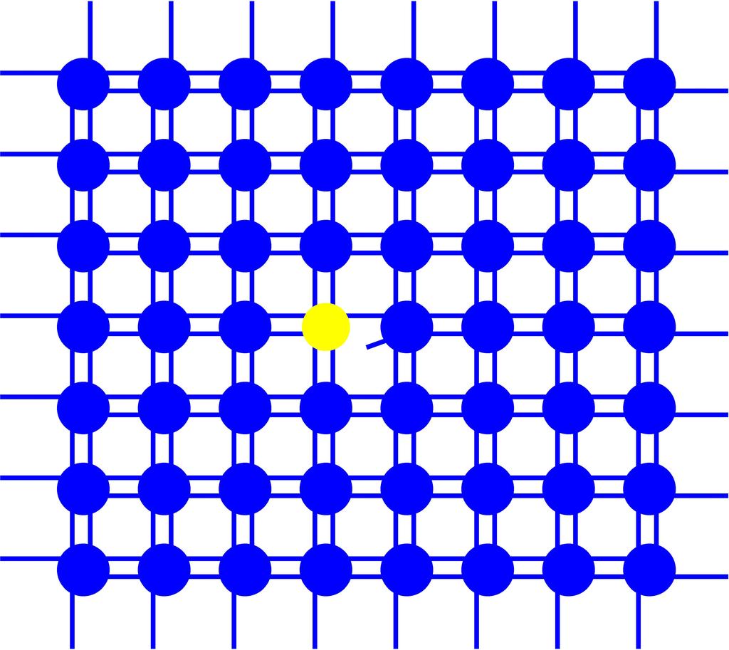
3 Donor impurity atom: Consider adding a group IV element as a substitutional impurity to silicon. Example: P, As, Sb in Si The fifth valence electron is denoted as a donor electron, and a donor impurity atom donates an electron to the conduction band.
4 The electron in the conduction band can now move through the crystal generating a current, while the positively charged ion is fixed in the crystal.
5 Concept of a Donor adding extra electrons: Band diagram equivalent view The energy level, E D, is the energy state of the donor electron. The donor impurity atoms add electrons to the conduction band without creating holes in the valence band. The resulting material is referred to as an n-type semiconductor (n for the negatively charged electron).
6 Acceptor impurity atom: consider adding a group III element as a substitutional impurity to silicon. One covalent bonding position appears to be empty. Example: B, Al, In in Si One less bond means the acceptor is electrically satisfied One less bond means the neighboring silicon is left with an empty state.
7
8 The "empty" position associated with the boron atom becomes occupied, and other valence electron positions become vacated. These other vacated electron positions can be thought of as holes in the semiconductor material. +
9 The hole can move through the crystal generating a current, while the negatively charged boron atom is fixed in the crystal. +
10 The hole can move through the crystal generating a current, while the negatively charged boron atom is fixed in the crystal. +
11 Concept of an Acceptor adding extra hole : Band diagram equivalent view The electron occupying the "empty" position does not have sufficient energy to be in the conduction band, so its energy is far smaller than the conductionband energy. The energy level, E A, is the energy state of the acceptor electron. The group III atom accepts an electron from the valence band and so is referred to as an acceptor impurity atom. This type of material is referred to as a p-type semiconductor (p for the positively charged hole).
12 Equilibrium Distribution of Electrons and Holes in extrinsic semiconductor Adding donor or acceptor impurity atoms to a semiconductor will change the distribution of electrons and holes in the material. The Fermi energy level in a semiconductor changes as the electron and hole concentrations change and, again, the Fermi energy changes as donor or acceptor impurities are added. If the Fermi energy changes from near the midgap value, the density of electrons in the conduction band and the density of holes in the valence band will change.
13
14
15 In an n-type semiconductor where n o > p o, electrons are referred to as the majority carrier and holes as the minority carrier. In a p-type semiconductor where p o > n o, holes are the majority carrier and electrons are the minority carrier. The thermal-equilibrium electron concentration in the extrinsic semiconductor can be written as which leads to If E F > E Fi, n-type Similarly, we have If E F < E Fi, p-type
16 The n o p o Product becomes which may be written as This product is always a constant for a given semiconductor material at a given temperature.
17 Statistics of donors and acceptors The probability statistics of donors and acceptors describe probability that a particular energy state, i. e., the donor and acceptor energy states, will be occupied by an electron. The probability function of electrons occupying the donor state is given as follows: where n d is the density of electrons occupying the donor level and E d is the energy of the donor level.
18 The above equation can also be written in the form where N d + is the concentration of ionized donors. Similarly, where N a is the concentration of acceptor atoms, E a is the acceptor energy level, p a is the concentration of holes in the acceptor states, and N a - is the concentration of ionized acceptors.
19 The ratio of electron the donor state to the total number of electrons in the conduction band plus donor state becomes where the factor (E c - E d ) is just the ionization energy of the donor electrons. At room temperature, the donor states are essentially completely ionized and, almost all donor impurity atoms have donated an electron to the conduction band.
20 Similarly, the ratio of holes in the acceptor state to the total number of holes in the valence band plus acceptor state becomes
21 The charge neutrality condition for a compensated semiconductor is expressed by equating the density of charges to the density of positive charges, and hence we have where n o and p o are the thermal-equilibrium concentrations of electrons and holes in the conduction band and valence band, respectively. The electron and hole concentration can be determined in terms of donor and acceptor atoms, or impurities, as follows: *A compensated semiconductor is one that contains both donor and acceptor impurity atoms in the same region.
 lc oiie acceptors --- -- - -- E {1 -- --- LZJI - -11-2\"\"\"'I?-.--.-l.i\"l\"P'Ll\"\"!!'!\"'. i---, -.. - +..L_ +...., -...J.....I:. + +,-... ----.....-. E L, T'\" T' 'T' - _.")
22 Thermal ejeclrons. Tota -1ectron i;:once(tration n.(} Donor electj"ons E.c - Ed + lj n... i 011jzeJ. donors E Fi U n-i n.i2 d 3Cceptors N - :;:= (N ri -p r1 ) lc oiie acceptors E { LZJI """'I?-.--.-l.i"l"P'Ll""!!'!"'. i---, L_ +...., -...J.....I:. + +, E L, T'" T' 'T' - _..,... l'o \----, r --'
23 POSITION OF FERMI ENERGY LEVEL (A) w.r.t. donor/acceptor impurities For n-type semiconductor in which N d >> n i, As the donor concentration increases, the Fermi level moves closer to the conduction band. For a p-type semiconductor, As the acceptor concentration increases, the Fermi level moves closer to the valence band.
24 Nd (crri- 3 ) E, """'T"---"T", --- "T", ---"T", ----, ---, --, ntype p type Ev I t I I I I 1016 I
25 (B) w.r.t. temperature The intrinsic carrier concentration n i is a strong function of temperature, so that E f is a function of temperature also. As the temperature increases, n i increases, and E F moves closer to the intrinsic Fermi level. As the temperature increases, additional electron-hole pairs are thermally generated so that the n i term the previous equations may begin to dominate. The semiconductor will eventually lose its extrinsic characteristics.

26 At high temperature, the semiconductor material begins to lose its extrinsic characteristics and begins to behave more like an intrinsic semiconductor. At the low temperature where freeze-out occurs, the Fermi level goes above E d for the n-type material and below E a for the p-type material. At absolute zero degrees, all energy states below EF are full and all energy states above E F are empty.
EE 346: Semiconductor Devices
 EE 346: Semiconductor Devices Lecture - 6 02/06/2017 Tewodros A. Zewde 1 DENSTY OF STATES FUNCTON Since current is due to the flow of charge, an important step in the process is to determine the number
Lecture 1. OUTLINE Basic Semiconductor Physics. Reading: Chapter 2.1. Semiconductors Intrinsic (undoped) silicon Doping Carrier concentrations
 silicon Doping Carrier concentrations") Lecture 1 OUTLINE Basic Semiconductor Physics Semiconductors Intrinsic (undoped) silicon Doping Carrier concentrations Reading: Chapter 2.1 EE105 Fall 2007 Lecture 1, Slide 1 What is a Semiconductor? Low
Lecture 1 OUTLINE Basic Semiconductor Physics Semiconductors Intrinsic (undoped) silicon Doping Carrier concentrations Reading: Chapter 2.1 EE105 Fall 2007 Lecture 1, Slide 1 What is a Semiconductor? Low
The Semiconductor in Equilibrium
 Lecture 6 Semiconductor physics IV The Semiconductor in Equilibrium Equilibrium, or thermal equilibrium No external forces such as voltages, electric fields. Magnetic fields, or temperature gradients are
EECS130 Integrated Circuit Devices
 EECS130 Integrated Circuit Devices Professor Ali Javey 8/30/2007 Semiconductor Fundamentals Lecture 2 Read: Chapters 1 and 2 Last Lecture: Energy Band Diagram Conduction band E c E g Band gap E v Valence
ECE 442. Spring, Lecture -2
 ECE 442 Power Semiconductor Devices and Integrated circuits Spring, 2006 University of Illinois at Chicago Lecture -2 Semiconductor physics band structures and charge carriers 1. What are the types of
Semiconductors 1. Explain different types of semiconductors in detail with necessary bond diagrams. Intrinsic semiconductors:
 Semiconductors 1. Explain different types of semiconductors in detail with necessary bond diagrams. There are two types of semi conductors. 1. Intrinsic semiconductors 2. Extrinsic semiconductors Intrinsic
Charge Carriers in Semiconductor
 Charge Carriers in Semiconductor To understand PN junction s IV characteristics, it is important to understand charge carriers behavior in solids, how to modify carrier densities, and different mechanisms
Lecture 3b. Bonding Model and Dopants. Reading: (Cont d) Notes and Anderson 2 sections
 Notes and Anderson 2 sections") Lecture 3b Bonding Model and Dopants Reading: (Cont d) Notes and Anderson 2 sections 2.3-2.7 The need for more control over carrier concentration Without help the total number of carriers (electrons and
Lecture 3b Bonding Model and Dopants Reading: (Cont d) Notes and Anderson 2 sections 2.3-2.7 The need for more control over carrier concentration Without help the total number of carriers (electrons and
Lecture 7: Extrinsic semiconductors - Fermi level
 Lecture 7: Extrinsic semiconductors - Fermi level Contents 1 Dopant materials 1 2 E F in extrinsic semiconductors 5 3 Temperature dependence of carrier concentration 6 3.1 Low temperature regime (T < T
Lecture 2 - Carrier Statistics in Equilibrium. September 5, 2002
 6.720J/3.43J Integrated Microelectronic Devices Fall 2002 Lecture 21 Lecture 2 Carrier Statistics in Equilibrium Contents: September 5, 2002 1. Conduction and valence bands, bandgap, holes 2. Intrinsic
Recitation 2: Equilibrium Electron and Hole Concentration from Doping
 Recitation : Equilibrium Electron and Hole Concentration from Doping Here is a list of new things we learned yesterday: 1. Electrons and Holes. Generation and Recombination 3. Thermal Equilibrium 4. Law
Key Questions. ECE 340 Lecture 6 : Intrinsic and Extrinsic Material I 9/10/12. Class Outline: Effective Mass Intrinsic Material
 9/1/1 ECE 34 Lecture 6 : Intrinsic and Extrinsic Material I Class Outline: Things you should know when you leave Key Questions What is the physical meaning of the effective mass What does a negative effective
First-Hand Investigation: Modeling of Semiconductors
 perform an investigation to model the behaviour of semiconductors, including the creation of a hole or positive charge on the atom that has lost the electron and the movement of electrons and holes in
smal band gap Saturday, April 9, 2011
 small band gap upper (conduction) band empty small gap valence band filled 2s 2p 2s 2p hybrid (s+p)band 2p no gap 2s (depend on the crystallographic orientation) extrinsic semiconductor semi-metal electron
EE143 Fall 2016 Microfabrication Technologies. Evolution of Devices
 EE143 Fall 2016 Microfabrication Technologies Prof. Ming C. Wu wu@eecs.berkeley.edu 511 Sutardja Dai Hall (SDH) 1-1 Evolution of Devices Yesterday s Transistor (1947) Today s Transistor (2006) 1-2 1 Why
CLASS 12th. Semiconductors
 CLASS 12th Semiconductors 01. Distinction Between Metals, Insulators and Semi-Conductors Metals are good conductors of electricity, insulators do not conduct electricity, while the semiconductors have
Lecture 2. Semiconductor Physics. Sunday 4/10/2015 Semiconductor Physics 1-1
 Lecture 2 Semiconductor Physics Sunday 4/10/2015 Semiconductor Physics 1-1 Outline Intrinsic bond model: electrons and holes Charge carrier generation and recombination Intrinsic semiconductor Doping:
EXTRINSIC SEMICONDUCTOR
 EXTRINSIC SEMICONDUCTOR EXTRINSIC SEMICONDUCTOR A semiconductor in which the impurity atoms are added by doping process is called Extrinsic semiconductor. The addition of impurities increases the carrier
Basic Semiconductor Physics
 6 Basic Semiconductor Physics 6.1 Introduction With this chapter we start with the discussion of some important concepts from semiconductor physics, which are required to understand the operation of solar
ECE 335: Electronic Engineering Lecture 2: Semiconductors
 Faculty of Engineering ECE 335: Electronic Engineering Lecture 2: Semiconductors Agenda Intrinsic Semiconductors Extrinsic Semiconductors N-type P-type Carrier Transport Drift Diffusion Semiconductors
Atoms? All matters on earth made of atoms (made up of elements or combination of elements).
.") Chapter 1 Atoms? All matters on earth made of atoms (made up of elements or combination of elements). Atomic Structure Atom is the smallest particle of an element that can exist in a stable or independent
Chapter 1 Atoms? All matters on earth made of atoms (made up of elements or combination of elements). Atomic Structure Atom is the smallest particle of an element that can exist in a stable or independent
EECS143 Microfabrication Technology
 EECS143 Microfabrication Technology Professor Ali Javey Introduction to Materials Lecture 1 Evolution of Devices Yesterday s Transistor (1947) Today s Transistor (2006) Why Semiconductors? Conductors e.g
Variation of Energy Bands with Alloy Composition E
 Variation of Energy Bands with Alloy Composition E 3.0 E.8.6 L 0.3eV Al x GaAs AlAs 1- xas 1.43eV.16eV X k.4 L. X.0 X 1.8 L 1.6 1.4 0 0. 0.4 0.6 X 0.8 1 1 Carriers in intrinsic Semiconductors Ec 4º 1º
Lecture 2 Electrons and Holes in Semiconductors
 EE 471: Transport Phenomena in Solid State Devices Spring 2018 Lecture 2 Electrons and Holes in Semiconductors Bryan Ackland Department of Electrical and Computer Engineering Stevens Institute of Technology
Review of Semiconductor Fundamentals
 ECE 541/ME 541 Microelectronic Fabrication Techniques Review of Semiconductor Fundamentals Zheng Yang (ERF 3017, email: yangzhen@uic.edu) Page 1 Semiconductor A semiconductor is an almost insulating material,
Ch. 2: Energy Bands And Charge Carriers In Semiconductors
 Ch. 2: Energy Bands And Charge Carriers In Semiconductors Discrete energy levels arise from balance of attraction force between electrons and nucleus and repulsion force between electrons each electron
Carriers Concentration in Semiconductors - V. Prof.P. Ravindran, Department of Physics, Central University of Tamil Nadu, India
 Carriers Concentration in Semiconductors - V 1 Prof.P. Ravindran, Department of Physics, Central University of Tamil Nadu, India http://folk.uio.no/ravi/semi2013 Motion and Recombination of Electrons and
Chapter 1 Semiconductor basics
 Chapter 1 Semiconductor basics ELEC-H402/CH1: Semiconductor basics 1 Basic semiconductor concepts Semiconductor basics Semiconductors, silicon and hole-electron pair Intrinsic silicon properties Doped
ELECTRONIC I Lecture 1 Introduction to semiconductor. By Asst. Prof Dr. Jassim K. Hmood
 ELECTRONIC I Lecture 1 Introduction to semiconductor By Asst. Prof Dr. Jassim K. Hmood SOLID-STATE ELECTRONIC MATERIALS Electronic materials generally can be divided into three categories: insulators,
Electrical Resistance
 Electrical Resistance I + V _ W Material with resistivity ρ t L Resistance R V I = L ρ Wt (Unit: ohms) where ρ is the electrical resistivity 1 Adding parts/billion to parts/thousand of dopants to pure
Electro - Principles I
 Electro - Principles I Page 10-1 Atomic Theory It is necessary to know what goes on at the atomic level of a semiconductor so the characteristics of the semiconductor can be understood. In many cases a
Semiconductor Devices and Circuits Fall Midterm Exam. Instructor: Dr. Dietmar Knipp, Professor of Electrical Engineering. Name: Mat. -Nr.
 Semiconductor Devices and Circuits Fall 2003 Midterm Exam Instructor: Dr. Dietmar Knipp, Professor of Electrical Engineering Name: Mat. -Nr.: Guidelines: Duration of the Midterm: 1 hour The exam is a closed
Lecture 2 - Carrier Statistics in Equilibrium. February 8, 2007
 6.720J/3.43J Integrated Microelectronic Devices Spring 2007 Lecture 21 Lecture 2 Carrier Statistics in Equilibrium Contents: February 8, 2007 1. Conduction and valence bands, bandgap, holes 2. Intrinsic
ECE 340 Lecture 6 : Intrinsic and Extrinsic Material I Class Outline:
 ECE 340 Lecture 6 : Intrinsic and Extrinsic Material I Class Outline: Effective Mass Intrinsic Material Extrinsic Material Things you should know when you leave Key Questions What is the physical meaning
PN Junction
 P Junction 2017-05-04 Definition Power Electronics = semiconductor switches are used Analogue amplifier = high power loss 250 200 u x 150 100 u Udc i 50 0 0 50 100 150 200 250 300 350 400 i,u dc i,u u
Semiconductor Physics fall 2012 problems
 Semiconductor Physics fall 2012 problems 1. An n-type sample of silicon has a uniform density N D = 10 16 atoms cm -3 of arsenic, and a p-type silicon sample has N A = 10 15 atoms cm -3 of boron. For each
n N D n p = n i p N A
 Summary of electron and hole concentration in semiconductors Intrinsic semiconductor: E G n kt i = pi = N e 2 0 Donor-doped semiconductor: n N D where N D is the concentration of donor impurity Acceptor-doped
A semiconductor is an almost insulating material, in which by contamination (doping) positive or negative charge carriers can be introduced.
 positive or negative charge carriers can be introduced.") Semiconductor A semiconductor is an almost insulating material, in which by contamination (doping) positive or negative charge carriers can be introduced. Page 2 Semiconductor materials Page 3 Energy levels
Semiconductor A semiconductor is an almost insulating material, in which by contamination (doping) positive or negative charge carriers can be introduced. Page 2 Semiconductor materials Page 3 Energy levels
Numerical Example: Carrier Concentrations
 2 Numerical ample: Carrier Concentrations Donor concentration: N d = 10 15 cm -3 Thermal equilibrium electron concentration: n o N d = 10 15 cm 3 Thermal equilibrium hole concentration: 2 2 p o = n i no
EE 446/646 Photovoltaic Devices I. Y. Baghzouz
 EE 446/646 Photovoltaic Devices I Y. Baghzouz What is Photovoltaics? First used in about 1890, the word has two parts: photo, derived from the Greek word for light, volt, relating to electricity pioneer
ECE 250 Electronic Devices 1. Electronic Device Modeling
 ECE 250 Electronic Devices 1 ECE 250 Electronic Device Modeling ECE 250 Electronic Devices 2 Introduction to Semiconductor Physics You should really take a semiconductor device physics course. We can only
Semiconductors. Semiconductors also can collect and generate photons, so they are important in optoelectronic or photonic applications.
 Semiconductors Semiconducting materials have electrical properties that fall between true conductors, (like metals) which are always highly conducting and insulators (like glass or plastic or common ceramics)
The photovoltaic effect occurs in semiconductors where there are distinct valence and
 How a Photovoltaic Cell Works The photovoltaic effect occurs in semiconductors where there are distinct valence and conduction bands. (There are energies at which electrons can not exist within the solid)
Semiconductor physics I. The Crystal Structure of Solids
 Lecture 3 Semiconductor physics I The Crystal Structure of Solids 1 Semiconductor materials Types of solids Space lattices Atomic Bonding Imperfection and doping in SOLIDS 2 Semiconductor Semiconductors
CLASS 1 & 2 REVISION ON SEMICONDUCTOR PHYSICS. Reference: Electronic Devices by Floyd
 CLASS 1 & 2 REVISION ON SEMICONDUCTOR PHYSICS Reference: Electronic Devices by Floyd 1 ELECTRONIC DEVICES Diodes, transistors and integrated circuits (IC) are typical devices in electronic circuits. All
EE301 Electronics I , Fall
 EE301 Electronics I 2018-2019, Fall 1. Introduction to Microelectronics (1 Week/3 Hrs.) Introduction, Historical Background, Basic Consepts 2. Rewiev of Semiconductors (1 Week/3 Hrs.) Semiconductor materials
Solid State Electronics EC210 Arab Academy for Science and Technology AAST Cairo Fall Lecture 10: Semiconductors
 Solid State Electronics EC210 Arab Academy for Science and Technology AAST Cairo Fall 2014 Lecture 10: Semiconductors Lecture Notes Prepared by: Dr. Amr Bayoumi, Dr. Nadia Rafat These PowerPoint color
EE495/695 Introduction to Semiconductors I. Y. Baghzouz ECE Department UNLV
 EE495/695 Introduction to Semiconductors I Y. Baghzouz ECE Department UNLV Introduction Solar cells have always been aligned closely with other electronic devices. We will cover the basic aspects of semiconductor
Lecture (02) Introduction to Electronics II, PN Junction and Diodes I
 Introduction to Electronics II, PN Junction and Diodes I") Lecture (02) Introduction to Electronics II, PN Junction and Diodes I By: Dr. Ahmed ElShafee ١ Agenda Current in semiconductors/conductors N type, P type semiconductors N Type Semiconductor P Type Semiconductor
Lecture (02) Introduction to Electronics II, PN Junction and Diodes I By: Dr. Ahmed ElShafee ١ Agenda Current in semiconductors/conductors N type, P type semiconductors N Type Semiconductor P Type Semiconductor
Crystal Properties. MS415 Lec. 2. High performance, high current. ZnO. GaN
 Crystal Properties Crystal Lattices: Periodic arrangement of atoms Repeated unit cells (solid-state) Stuffing atoms into unit cells Determine mechanical & electrical properties High performance, high current
Diamond. Covalent Insulators and Semiconductors. Silicon, Germanium, Gray Tin. Chem 462 September 24, 2004
 Covalent Insulators and Chem 462 September 24, 2004 Diamond Pure sp 3 carbon All bonds staggered- ideal d(c-c) - 1.54 Å, like ethane Silicon, Germanium, Gray Tin Diamond structure Si and Ge: semiconductors
Introduction to Engineering Materials ENGR2000. Dr.Coates
 Introduction to Engineering Materials ENGR2000 Chapter 18: Electrical Properties Dr.Coates 18.2 Ohm s Law V = IR where R is the resistance of the material, V is the voltage and I is the current. l R A
ESE 372 / Spring 2013 / Lecture 5 Metal Oxide Semiconductor Field Effect Transistor
 Metal Oxide Semiconductor Field Effect Transistor V G V G 1 Metal Oxide Semiconductor Field Effect Transistor We will need to understand how this current flows through Si What is electric current? 2 Back
SEMICONDUCTOR PHYSICS
 SEMICONDUCTOR PHYSICS by Dibyendu Chowdhury Semiconductors The materials whose electrical conductivity lies between those of conductors and insulators, are known as semiconductors. Silicon Germanium Cadmium
MTLE-6120: Advanced Electronic Properties of Materials. Intrinsic and extrinsic semiconductors. Reading: Kasap:
 MTLE-6120: Advanced Electronic Properties of Materials 1 Intrinsic and extrinsic semiconductors Reading: Kasap: 5.1-5.6 Band structure and conduction 2 Metals: partially filled band(s) i.e. bands cross
Electronic PRINCIPLES
 MALVINO & BATES Electronic PRINCIPLES SEVENTH EDITION Chapter 2 Semiconductors Topics Covered in Chapter 2 Conductors Semiconductors Silicon crystals Intrinsic semiconductors Two types of flow Doping a
! Previously: simple models (0 and 1 st order) " Comfortable with basic functions and circuits. ! This week and next (4 lectures)
 Comfortable with basic functions and circuits. ! This week and next (4 lectures)") ESE370: CircuitLevel Modeling, Design, and Optimization for Digital Systems Lec 6: September 14, 2015 MOS Model You are Here: Transistor Edition! Previously: simple models (0 and 1 st order) " Comfortable
ESE370: CircuitLevel Modeling, Design, and Optimization for Digital Systems Lec 6: September 14, 2015 MOS Model You are Here: Transistor Edition! Previously: simple models (0 and 1 st order) " Comfortable
Due to the quantum nature of electrons, one energy state can be occupied only by one electron.
 In crystalline solids, not all values of the electron energy are possible. The allowed intervals of energy are called allowed bands (shown as blue and chess-board blue). The forbidden intervals are called
Chemistry Instrumental Analysis Lecture 8. Chem 4631
 Chemistry 4631 Instrumental Analysis Lecture 8 UV to IR Components of Optical Basic components of spectroscopic instruments: stable source of radiant energy transparent container to hold sample device
Mark Lundstrom 2/10/2013. SOLUTIONS: ECE 606 Homework Week 5 Mark Lundstrom Purdue University (corrected 3/26/13)
") SOLUIONS: ECE 606 Homework Week 5 Mark Lundstrom Purdue University corrected 6/13) Some of the problems below are taken/adapted from Chapter 4 in Advanced Semiconductor Fundamentals, nd. Ed. By R.F. Pierret.
SOLUIONS: ECE 606 Homework Week 5 Mark Lundstrom Purdue University corrected 6/13) Some of the problems below are taken/adapted from Chapter 4 in Advanced Semiconductor Fundamentals, nd. Ed. By R.F. Pierret.
Ga and P Atoms to Covalent Solid GaP
 Ga and P Atoms to Covalent Solid GaP Band Gaps in Binary Group III-V Semiconductors Mixed Semiconductors Affect of replacing some of the As with P in GaAs Band Gap (ev) (nm) GaAs 1.35 919 (IR) GaP 2.24
Engineering 2000 Chapter 8 Semiconductors. ENG2000: R.I. Hornsey Semi: 1
 Engineering 2000 Chapter 8 Semiconductors ENG2000: R.I. Hornsey Semi: 1 Overview We need to know the electrical properties of Si To do this, we must also draw on some of the physical properties and we
The German University in Cairo. Faculty of Information Engineering & Technology Semiconductors (Elct 503) Electronics Department Fall 2014
 Electronics Department Fall 2014") The German University in Cairo th Electronics 5 Semester Faculty of Information Engineering & Technology Semiconductors (Elct 503) Electronics Department Fall 2014 Problem Set 3 1- a) Find the resistivity
The German University in Cairo th Electronics 5 Semester Faculty of Information Engineering & Technology Semiconductors (Elct 503) Electronics Department Fall 2014 Problem Set 3 1- a) Find the resistivity
Lecture (02) PN Junctions and Diodes
 PN Junctions and Diodes") Lecture (02) PN Junctions and Diodes By: Dr. Ahmed ElShafee ١ I Agenda N type, P type semiconductors N Type Semiconductor P Type Semiconductor PN junction Energy Diagrams of the PN Junction and Depletion
Lecture (02) PN Junctions and Diodes By: Dr. Ahmed ElShafee ١ I Agenda N type, P type semiconductors N Type Semiconductor P Type Semiconductor PN junction Energy Diagrams of the PN Junction and Depletion
ECE 142: Electronic Circuits Lecture 3: Semiconductors
 Faculty of Engineering ECE 142: Electronic Circuits Lecture 3: Semiconductors Agenda Intrinsic Semiconductors Extrinsic Semiconductors N-type P-type Carrier Transport Drift Diffusion Semiconductors A semiconductor
Intrinsic Semiconductors
 Technische Universität Graz Institute of Solid State Physics Intrinsic Semiconductors ermi function f(e) is the probability that a state at energy E is occupied. f( E) 1 E E 1 exp kt B ermi energy The
Chapter 1 Overview of Semiconductor Materials and Physics
 Chapter 1 Overview of Semiconductor Materials and Physics Professor Paul K. Chu Conductivity / Resistivity of Insulators, Semiconductors, and Conductors Semiconductor Elements Period II III IV V VI 2 B
UNIVERSITY OF CALIFORNIA College of Engineering Department of Electrical Engineering and Computer Sciences. EECS 130 Professor Ali Javey Fall 2006
 UNIVERSITY OF CALIFORNIA College of Engineering Department of Electrical Engineering and Computer Sciences EECS 130 Professor Ali Javey Fall 2006 Midterm I Name: Closed book. One sheet of notes is allowed.
LECTURE 23. MOS transistor. 1 We need a smart switch, i.e., an electronically controlled switch. Lecture Digital Circuits, Logic
 LECTURE 23 Lecture 16-20 Digital Circuits, Logic 1 We need a smart switch, i.e., an electronically controlled switch 2 We need a gain element for example, to make comparators. The device of our dreams
KATIHAL FİZİĞİ MNT-510
 KATIHAL FİZİĞİ MNT-510 YARIİLETKENLER Kaynaklar: Katıhal Fiziği, Prof. Dr. Mustafa Dikici, Seçkin Yayıncılık Katıhal Fiziği, Şakir Aydoğan, Nobel Yayıncılık, Physics for Computer Science Students: With
electronics fundamentals
 electronics fundamentals circuits, devices, and applications THOMAS L. FLOYD DAVID M. BUCHLA Lesson 1: Diodes and Applications Semiconductors Figure 1-1 The Bohr model of an atom showing electrons in orbits
The Periodic Table III IV V
 The Periodic Table III IV V Slide 1 Electronic Bonds in Silicon 2-D picture of perfect crystal of pure silicon; double line is a Si-Si bond with each line representing an electron Si ion (charge +4 q)
ECE 440 Lecture 20 : PN Junction Electrostatics II Class Outline:
 ECE 440 Lecture 20 : PN Junction Electrostatics II Class Outline: Depletion Approximation Step Junction Things you should know when you leave Key Questions What is the space charge region? What are the
Doped Semiconductors *
 OpenStax-CNX module: m1002 1 Doped Semiconductors * Bill Wilson This work is produced by OpenStax-CNX and licensed under the Creative Commons Attribution License 1.0 To see how we can make silicon a useful
! Previously: simple models (0 and 1 st order) " Comfortable with basic functions and circuits. ! This week and next (4 lectures)
 Comfortable with basic functions and circuits. ! This week and next (4 lectures)") ESE370: CircuitLevel Modeling, Design, and Optimization for Digital Systems Lec 6: September 18, 2017 MOS Model You are Here: Transistor Edition! Previously: simple models (0 and 1 st order) " Comfortable
ESE370: CircuitLevel Modeling, Design, and Optimization for Digital Systems Lec 6: September 18, 2017 MOS Model You are Here: Transistor Edition! Previously: simple models (0 and 1 st order) " Comfortable
EE 5211 Analog Integrated Circuit Design. Hua Tang Fall 2012
 EE 5211 Analog Integrated Circuit Design Hua Tang Fall 2012 Today s topic: 1. Introduction to Analog IC 2. IC Manufacturing (Chapter 2) Introduction What is Integrated Circuit (IC) vs discrete circuits?
n i exp E g 2kT lnn i E g 2kT
 HOMEWORK #10 12.19 For intrinsic semiconductors, the intrinsic carrier concentration n i depends on temperature as follows: n i exp E g 2kT (28.35a) or taking natural logarithms, lnn i E g 2kT (12.35b)
Processing of Semiconducting Materials Prof. Pallab Banerji Department of Material Science Indian Institute of Technology, Kharagpur
 Processing of Semiconducting Materials Prof. Pallab Banerji Department of Material Science Indian Institute of Technology, Kharagpur Lecture - 4 Doping in Semiconductors Good morning. Let us start with
Semiconductor Physics. Lecture 3
 Semiconductor Physics Lecture 3 Intrinsic carrier density Intrinsic carrier density Law of mass action Valid also if we add an impurity which either donates extra electrons or holes the number of carriers
ESE370: Circuit-Level Modeling, Design, and Optimization for Digital Systems
 ESE370: Circuit-Level Modeling, Design, and Optimization for Digital Systems Lec 6: September 14, 2015 MOS Model You are Here: Transistor Edition! Previously: simple models (0 and 1 st order) " Comfortable
Chapter 2. Electronics I - Semiconductors
 Chapter 2 Electronics I - Semiconductors Fall 2017 talarico@gonzaga.edu 1 Charged Particles The operation of all electronic devices is based on controlling the flow of charged particles There are two type
Chapter 12: Semiconductors
 Chapter 12: Semiconductors Bardeen & Shottky January 30, 2017 Contents 1 Band Structure 4 2 Charge Carrier Density in Intrinsic Semiconductors. 6 3 Doping of Semiconductors 12 4 Carrier Densities in Doped
ECE 606 Homework Week 7 Mark Lundstrom Purdue University (revised 2/25/13) e E i! E T
 e E i! E T") ECE 606 Homework Week 7 Mark Lundstrom Purdue University (revised 2/25/13) 1) Consider an n- type semiconductor for which the only states in the bandgap are donor levels (i.e. ( E T = E D ). Begin with
ECE 606 Homework Week 7 Mark Lundstrom Purdue University (revised 2/25/13) 1) Consider an n- type semiconductor for which the only states in the bandgap are donor levels (i.e. ( E T = E D ). Begin with
Mat E 272 Lecture 25: Electrical properties of materials
 Mat E 272 Lecture 25: Electrical properties of materials December 6, 2001 Introduction: Calcium and copper are both metals; Ca has a valence of +2 (2 electrons per atom) while Cu has a valence of +1 (1
Chapter 2. Semiconductor Fundamentals
 hapter Semiconductor Fundamentals.0 Introduction There are altogether 9 types of natural occurring elements, of which only few types are important in semiconductor physics and technology. They are the
Electrons are shared in covalent bonds between atoms of Si. A bound electron has the lowest energy state.
 Photovoltaics Basic Steps the generation of light-generated carriers; the collection of the light-generated carriers to generate a current; the generation of a large voltage across the solar cell; and
Introduction to Semiconductor Physics. Prof.P. Ravindran, Department of Physics, Central University of Tamil Nadu, India
 Introduction to Semiconductor Physics 1 Prof.P. Ravindran, Department of Physics, Central University of Tamil Nadu, India http://folk.uio.no/ravi/cmp2013 Review of Semiconductor Physics Semiconductor fundamentals
Session 5: Solid State Physics. Charge Mobility Drift Diffusion Recombination-Generation
 Session 5: Solid State Physics Charge Mobility Drift Diffusion Recombination-Generation 1 Outline A B C D E F G H I J 2 Mobile Charge Carriers in Semiconductors Three primary types of carrier action occur
Bohr s Model, Energy Bands, Electrons and Holes
 Dual Character of Material Particles Experimental physics before 1900 demonstrated that most of the physical phenomena can be explained by Newton's equation of motion of material particles or bodies and
PHYS208 p-n junction. January 15, 2010
 1 PHYS208 p-n junction January 15, 2010 List of topics (1) Density of states Fermi-Dirac distribution Law of mass action Doped semiconductors Dopinglevel p-n-junctions 1 Intrinsic semiconductors List of
CHAPTER 2: ENERGY BANDS & CARRIER CONCENTRATION IN THERMAL EQUILIBRIUM. M.N.A. Halif & S.N. Sabki
 CHAPTER 2: ENERGY BANDS & CARRIER CONCENTRATION IN THERMAL EQUILIBRIUM OUTLINE 2.1 INTRODUCTION: 2.1.1 Semiconductor Materials 2.1.2 Basic Crystal Structure 2.1.3 Basic Crystal Growth technique 2.1.4 Valence
Basic cell design. Si cell
 Basic cell design Si cell 1 Concepts needed to describe photovoltaic device 1. energy bands in semiconductors: from bonds to bands 2. free carriers: holes and electrons, doping 3. electron and hole current:
Semiconductor Physics
 Semiconductor Physics Motivation Is it possible that there might be current flowing in a conductor (or a semiconductor) even when there is no potential difference supplied across its ends? Look at the
Chapter 7. The pn Junction
 Chapter 7 The pn Junction Chapter 7 PN Junction PN junction can be fabricated by implanting or diffusing donors into a P-type substrate such that a layer of semiconductor is converted into N type. Converting
Introduction to Transistors. Semiconductors Diodes Transistors
 Introduction to Transistors Semiconductors Diodes Transistors 1 Semiconductors Typical semiconductors, like silicon and germanium, have four valence electrons which form atomic bonds with neighboring atoms
Note that it is traditional to draw the diagram for semiconductors rotated 90 degrees, i.e. the version on the right above.
 5 Semiconductors The nearly free electron model applies equally in the case where the Fermi level lies within a small band gap (semiconductors), as it does when the Fermi level lies within a band (metal)
1 Name: Student number: DEPARTMENT OF PHYSICS AND PHYSICAL OCEANOGRAPHY MEMORIAL UNIVERSITY OF NEWFOUNDLAND. Fall :00-11:00
 1 Name: DEPARTMENT OF PHYSICS AND PHYSICAL OCEANOGRAPHY MEMORIAL UNIVERSITY OF NEWFOUNDLAND Final Exam Physics 3000 December 11, 2012 Fall 2012 9:00-11:00 INSTRUCTIONS: 1. Answer all seven (7) questions.
Lecture 02 Semiconductor Physics
 Lecture 02 Semiconductor Physics Prepared By Dr. Eng. Sherif Hekal Assistant Professor, CCE department Lecture 02 Semiconductors 10/15/201 7 1 ILOS In this section, we will learn: The basic properties
PH575 Spring Lecture #19 Semiconductors: electrical & optical properties: Kittel Ch. 8 pp ; Ch. 20
 PH575 Spring 2014 Lecture #19 Semiconductors: electrical & optical properties: Kittel Ch. 8 pp. 205-214; Ch. 20 Simplified diagram of the filling of electronic band structure in various types of material,
5. Semiconductors and P-N junction
 5. Semiconductors and P-N junction Thomas Zimmer, University of Bordeaux, France Summary Learning Outcomes... 2 Physical background of semiconductors... 2 The silicon crystal... 2 The energy bands... 3