Atomistic simulations on the mobility of di- and tri-interstitials in Si
|
|
|
- Hilary Hunt
- 5 years ago
- Views:
Transcription
1 Atomistic simulations on the mobility of di- and tri-interstitials in Si related publications (since 2001): Posselt, M., Gao, F., Zwicker, D., Atomistic study of the migration of di- and tri-interstitials in silicon, Phys. Rev. B 71 (2005) Posselt, M., Gao, F., Zwicker, D, Migration of di- and tri-interstitials in silicon, Nucl. Instr. Meth. B 228 (2005) 212
2 methods to determine diffusion coefficients ssd a sum of the squared displacements of all atoms vs. time N ( t) = ( r ( t) r (0)) i= 1 i self-diffusion coefficient per defect D s i 2 = const. + 6D defect diffusivity D d s t D s : mobility of the lattice atoms due to the presence of the defect is obtained by monitoring the trajectory of the center-of-mass of the defect using the Wigner-Seitz-cell analysis trajectory is decomposed into n s segments for each segment m the squared displacement is calculated D d = 1 n d m= 1 6Δ (tracer) correlation factor s n s sd ( m) t sd t m d f = ( m) = ( R( t ) R( t = t D D m 1 s d + Δt m 2 m 1 )),
 E f = 6.")
 (1-10) (011) DFT: Richie")
: 6.")
3 di-interstitial structure and energetics I 2 A Z structure (C 2h ) E f = 6.10 ev E b = 1.74eV (110) (1-10) (011) DFT: Richie 2004: 6.46 ev CP: Gilmer 1995 (SW): 5.70 ev; Marques 2001 (T3): 6.32 ev TB: Rasband 1996: 8.0 ev; Hane 2000: 5.85 ev
 (1-10) similar configuration (found by TB and DFT): triangle in {111} (C 1h ) TB:")

4 I 2 B modified triangle in {111} (C 1h ) E f = 6.14 ev E b = 1.70 ev DFT: Richie 2004: 6.46 ev (111) (1-10) similar configuration (found by TB and DFT): triangle in {111} (C 1h ) TB: Rasband 1996: 7.3 ev; Hane 2000: 5.64 ev; Bongiorno 2000: 4.91 ev DFT: Kim 1999: ev; Jones 2002: 5.19 ev; Chichkine 2002: ev; Richie 2004: 5.66 ev; Lopez 2004: ev


5 I 2 C W structure (C 2v ) E f = 6.37 ev E b = 1.47 ev (110) (1-10) TB: Rasband 1996: 7.7 ev; Hane 2000: 6.07 ev

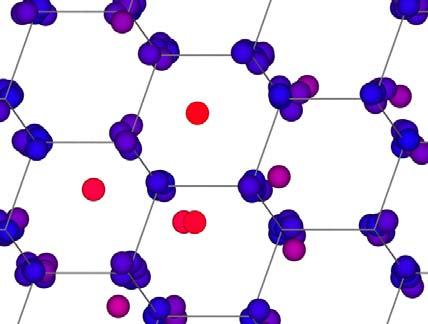
6 migration center of mass trajectories over a period of 4.4 ns 30 Å T = 800 K T = 1200 K temperature dependent migration mechanism T = 1600 K low T high mobility along <110> axes, change between equivalent directions occurs seldom and requires a long time high T frequent change between equivalent <110> directions

7 migration along <110>: in a {110} plane, as I 2 A... snapshots: migration distance: 2 nd n.n. distance 2 ps <110> {110} I 2 A I 2 A I 2 A

8 movie 1c (~3 ps) migration distance: 2nd n.n. distance {110} atoms belonging to the defect change continuously bond switching place the cursor on the figure and double click to start the movie
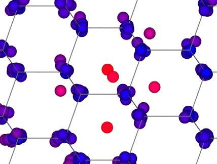
 I A 2 1 ps {110} a I 2 B {111} <111> <110> rotation out of the {111} plane")
9 change between different <110> directions ({110} planes) via transformation: I 2A I 2B (immobile) I A 2 1 ps {110} a I 2 B {111} <111> <110> rotation out of the {111} plane b


10 {110} <111> c {111} <110> d e I 2 A
11 detailed analysis of migration of the di-i rate for the change between different {110} planes T (K) diffusivity within the {110} planes ω d (s -1 ) T m = 1687 K 10-5 Dd 110 (cm 2 s -1 ) E a = 0.46 ev /kT (ev -1 ) 10-6 E a = 0.20 ev
12 T (K) diffusivity (cm 2 s -1 ) T m = 1687 K /kT (ev -1 ) D di-i d D di-i s D I d D I s E a = 0.22 ev E a = 0.38 ev E a = 0.98 ev highly mobile mono and di-i: defect mobility higher than atomic mobility
![structure and energetics I A 3 mod. tetrahedron (C 2v ) tri-interstitial [001] 1 2 E f = 7.54 ev E b = 4.](/docs-images/80/81766151/images/13-0.jpg "22 ev 3 4 near (110) near (1-10) CP: Gilmer 1995 (SW): 7.08 ev; Lenosky 2000 (EDIP): 8.")
: tetrahedron (C 2v ) TB: Bongiorno 2000: 6.")
13 structure and energetics I A 3 mod. tetrahedron (C 2v ) tri-interstitial [001] 1 2 E f = 7.54 ev E b = 4.22 ev 3 4 near (110) near (1-10) CP: Gilmer 1995 (SW): 7.08 ev; Lenosky 2000 (EDIP): 8.85 ev; Lenosky 2000 (L): 6.03 ev similar configuration (found by TB and DFT): tetrahedron (C 2v ) TB: Bongiorno 2000: 6.69 ev; Lenosky 2000: 7.83 DFT: Kim 2000: ~6 ev; Chichkine 2002: 6.05 ev; Richie 2004: ev; Lopez 2004: 7.27 ev
 [111] 1 E f = 7.")
 similar configuration (found")
14 I 3 B mod. bond-centered triple I (C 3v ) [111] 1 E f = 7.59 ev E b = 4.17 ev (111) similar configuration (found by DFT): bond-centered triple (C 3v ) DFT: Chichkine 2002: 6.09 ev; Lopez 2004: 7.32 ev

15 trajectories over a period of 14.4 ns migration T = 1400 K T = 1500 K T = 1600 K complex trajectories, e.g. around a six member ring


16 I 3 B I 3 A I 3 B a b c 35 ps d e f I 3 A

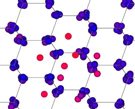

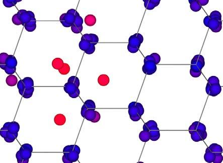
17 I 3 B g h i j k I 3 A I 3 B
18 T (K) diffusivity (cm 2 s -1 ) T m = 1687 K D di-i d D di-i s D I D tri-i s d D tri-i d D I s /kT (ev -1 ) E a = 0.22 ev E a = 0.38 ev E a = 1.8 ev E a = 1.7 ev E a = 0.98 ev tri-i: atomic mobility higher than defect mobility
19 comparison with experimental data (di- and tri-i) a) direct observation of di- and tri-i (?) EPR P6 center related to di-i? pro: Lee 1976, 1998 contra: Jones 2002 PL W center related to tri-i? pro: Jones 2002 contra: Lopez 2004
20 b) indirect proofs for the existence of di- and tri-i state-of-the-art description of defect evolution and TED of dopants (B) during post-implantation annealing: Cowern et al. 1999, Pelaz et al formation of interstitial clusters must be assumed During ion implantation only mono-interstitials and mono-vacancies are formed. Their concentration is much higher than in the thermodynamic equilibrium. but - atomistic simulations of defect formation reveal: large variety of as-implanted defects is formed (also di- and tri-i)
21 The mono-interstitial and the mono-vacancy are the only mobile intrinsic defects. They recombine or form immobile clusters. In particular self interstitial clusters - amongst them the di-interstitial -are introduced to obtain a transient storage of self-interstitials and to explain quantitatively the formation of {311} defects and dislocation loops as well as the TED but - present investigations: mobile di- and tri-i
22 Cowern : OR model for defect evolution start: only I kev Si S = D B /D eq B E b c = Q I E m I -E fc Q I ~ 4.5 ev E m I ~ 1 ev E b di-i ~ 2.2 ev E b tri-i ~ 2.3 ev 1.7 ev 2.5 ev E bc (n) non-monotonic 2 3 {113}
23 Pelaz : KMC simulation of defect evolution and TED start: V,I from BCA 40 kev Si E b di-i ~ 1.6 ev E b tri-i ~ 1.8 ev 1.7 ev 2.5 ev E bc (n) monotonic Aboy 2003: E bc (n) of Cowern E m I of Bracht
24 c) explanation of the long-range, trap-limited migration of implantation-induced I-like defects observed at room temperature by the high mobility of the di-i
25 Kyllesbech Larsen et al. 1996: implantation and ex-situ SRP measurements of deactivation 40 kev Si 5x10 13 cm -2 injection and trapping of I-like defects traps: epi: [O]<10 15 cm -3 ; [C]<10 15 cm -3 FZ: [O]~10 16 cm -3 ; [C]~10 17 cm -3 Cz: [O]~10 18 cm -3 ; [C]~10 17 cm -3 dopants deactivation a very low fraction (~10-5 ) of the ballistically formed defects is mobile and responsible for the deactivation
26 Collart 1998: implantation and in-situ resistivity measurement B (10 13 cm -2 ) sheet resistance 20 kev Ar, Si epi-si undoped (deposited) n 0.5 μm mobile I-like defects are formed during implantation
27 Privitera 1996: implantation and ex-situ SRP measurements epi: [O]<10 16 cm -3 ; [C]<10 16 cm -3 n (phosphorus) doped ~10 14 cm -3 Si implants: deactivation by I-like defects He implants: deactivation by V-like defects Si after He: reduction of deactivation by V-like defects due to injection and trapping of I-like defects
28 lower bounds of the diffusivity of the I-like defects: cm 2 s -1 (Kyllesbech Larsen, Privitera), 10-7 cm 2 s -1 (Collart) if this were the value for the mono-i diffusivity at RT: - about twenty orders of magnitude larger than D I (RT) obtained by diffusion experiments near the thermodynamic equilibrium (Bracht 1998 ). - much (5-10 orders of magnitude) larger than the mono-interstitial diffusivity often used in the interpretation of defect evolution and transition-enhanced diffusion of boron during post-implantation annealing (Pelaz 1997 ) - larger than many theoretical results (Colombo 2002) it could be the value for the di-i diffusivity (10-8 cm 2 s -1 )!
Atomistic Front-End Process Modeling
 Atomistic Front-End Process Modeling A Powerful Tool for Deep-Submicron Device Fabrication SISPAD 2001, Athens Martin Jaraiz University of Valladolid, Spain Thanks to: P. Castrillo (U. Valladolid) R. Pinacho
Multiscale modelling of D trapping in W
 CMS Multiscale modelling of D trapping in W Kalle Heinola, Tommy Ahlgren and Kai Nordlund Department of Physics and Helsinki Institute of Physics University of Helsinki, Finland Contents Background Plasma-wall
Joint ICTP-IAEA Workshop on Physics of Radiation Effect and its Simulation for Non-Metallic Condensed Matter.
 2359-3 Joint ICTP-IAEA Workshop on Physics of Radiation Effect and its Simulation for Non-Metallic Condensed Matter 13-24 August 2012 Electrically active defects in semiconductors induced by radiation
Lecture 1. OUTLINE Basic Semiconductor Physics. Reading: Chapter 2.1. Semiconductors Intrinsic (undoped) silicon Doping Carrier concentrations
 silicon Doping Carrier concentrations") Lecture 1 OUTLINE Basic Semiconductor Physics Semiconductors Intrinsic (undoped) silicon Doping Carrier concentrations Reading: Chapter 2.1 EE105 Fall 2007 Lecture 1, Slide 1 What is a Semiconductor? Low
Lecture 1 OUTLINE Basic Semiconductor Physics Semiconductors Intrinsic (undoped) silicon Doping Carrier concentrations Reading: Chapter 2.1 EE105 Fall 2007 Lecture 1, Slide 1 What is a Semiconductor? Low
Diffusion in Extrinsic Silicon and Silicon Germanium
 1 Diffusion in Extrinsic Silicon and Silicon Germanium SFR Workshop & Review November 14, 2002 Hughes Silvestri, Ian Sharp, Hartmut Bracht, and Eugene Haller Berkeley, CA 2002 GOAL: Diffusion measurements
Interaction of ion beams with matter
 Interaction of ion beams with matter Introduction Nuclear and electronic energy loss Radiation damage process Displacements by nuclear stopping Defects by electronic energy loss Defect-free irradiation
Simple atomistic modeling of dominant B m I n clusters in boron diffusion
 Molecular Simulation, Vol. 31, No. 12, 15 October 2005, 817 824 Simple atomistic modeling of dominant B m I n clusters in boron diffusion J.-H. YOO, C.-O. HWANG, B.-J. KIM and T. WON* Department of Electrical
DIFFUSION - Chapter 7
 DIFFUSION - Chapter 7 Doping profiles determine many short-channel characteristics in MOS devices. Resistance impacts drive current. Scaling implies all lateral and vertical dimensions scale by the same
2. Point Defects. R. Krause-Rehberg
 R. Krause-Rehberg 2. Point Defects (F-center in acl) 2.1 Introduction 2.2 Classification 2.3 otation 2.4 Examples 2.5 Peculiarities in Semiconductors 2.6 Determination of Structure and Concentration 2.7
EE 212 FALL ION IMPLANTATION - Chapter 8 Basic Concepts
 EE 212 FALL 1999-00 ION IMPLANTATION - Chapter 8 Basic Concepts Ion implantation is the dominant method of doping used today. In spite of creating enormous lattice damage it is favored because: Large range
Diffusion in Extrinsic Silicon
 1 Diffusion in Extrinsic Silicon SFR Workshop & Review April 17, 2002 Hughes Silvestri, Ian Sharp, Hartmut Bracht, and Eugene Haller Berkeley, CA 2002 GOAL: Diffusion measurements on P doped Si to complete
Electrically active defects in semiconductors induced by radiation
 Electrically active defects in semiconductors induced by radiation Ivana Capan Rudjer Boskovic Institute, Croatia http://www.irb.hr/users/capan Outline Radiation damage Capacitance transient techniques
Quiz #1 Practice Problem Set
 Name: Student Number: ELEC 3908 Physical Electronics Quiz #1 Practice Problem Set? Minutes January 22, 2016 - No aids except a non-programmable calculator - All questions must be answered - All questions
Review of Semiconductor Fundamentals
 ECE 541/ME 541 Microelectronic Fabrication Techniques Review of Semiconductor Fundamentals Zheng Yang (ERF 3017, email: yangzhen@uic.edu) Page 1 Semiconductor A semiconductor is an almost insulating material,
The annealing of interstitial carbon atoms in high resistivity n-type silicon after proton irradiation
 ROSE/TN/2002-01 The annealing of interstitial carbon atoms in high resistivity n-type silicon after proton irradiation M. Kuhnke a,, E. Fretwurst b, G. Lindstroem b a Department of Electronic and Computer
Identification of Getter Defects in high-energy self-implanted Silicon at Rp/2
 Identification of Getter Defects in high-energy self-implanted Silicon at Rp R. Krause-Rehberg 1, F. Börner 1, F. Redmann 1, J. Gebauer 1, R. Kögler 2, R. Kliemann 2, W. Skorupa 2, W. Egger 3, G. Kögel
F + Implants in Crystalline Si: The Si Interstitial Contribution
 Mater. Res. Soc. Symp. Proc. Vol. 1070 2008 Materials Research Society 1070-E06-07 F + Implants in Crystalline Si: The Si Interstitial Contribution Pedro Lopez 1, Lourdes Pelaz 1, Ray Duffy 2, P. Meunier-Beillard
Comparisons of DFT-MD, TB- MD and classical MD calculations of radiation damage and plasmawallinteractions
 CMS Comparisons of DFT-MD, TB- MD and classical MD calculations of radiation damage and plasmawallinteractions Kai Nordlund Department of Physics and Helsinki Institute of Physics University of Helsinki,
Abstract We combined several atomistic techniques to identify the structure of
 Journal of Electronic Materials manuscript No. (will be inserted by the editor) W and X photoluminescence centers in crystalline Si: chasing candidates at atomic level through multiscale simulations María
September 21, 2005, Wednesday
 , Wednesday Doping and diffusion I Faster MOSFET requires shorter channel P + Poly Al Al Motivation Requires shallower source, drain Al P + Poly Al source drain Shorter channel length; yes, but same source
A semiconductor is an almost insulating material, in which by contamination (doping) positive or negative charge carriers can be introduced.
 positive or negative charge carriers can be introduced.") Semiconductor A semiconductor is an almost insulating material, in which by contamination (doping) positive or negative charge carriers can be introduced. Page 2 Semiconductor materials Page 3 Energy levels
Semiconductor A semiconductor is an almost insulating material, in which by contamination (doping) positive or negative charge carriers can be introduced. Page 2 Semiconductor materials Page 3 Energy levels
Introduction to Semiconductor Physics. Prof.P. Ravindran, Department of Physics, Central University of Tamil Nadu, India
 Introduction to Semiconductor Physics 1 Prof.P. Ravindran, Department of Physics, Central University of Tamil Nadu, India http://folk.uio.no/ravi/cmp2013 Review of Semiconductor Physics Semiconductor fundamentals
Ion Implantation ECE723
 Ion Implantation Topic covered: Process and Advantages of Ion Implantation Ion Distribution and Removal of Lattice Damage Simulation of Ion Implantation Range of Implanted Ions Ion Implantation is the
Structure and dynamics of the diarsenic complex in crystalline silicon
 Structure and dynamics of the diarsenic complex in crystalline silicon Scott A. Harrison, Thomas F. Edgar, and Gyeong S. Hwang* Department of Chemical Engineering, University of Texas, Austin, Texas 78713,
Atomistic simulations of point defect diffusion in Si and SiGe
 Atomistic simulations of point defect diffusion in Si and SiGe P. Pochet, D. Caliste, K. Rushchanskii, F. Lançon & T. Deutsch CEA UJF INAC Institute for Nanoscience and Cryogenics Partially founded by
Dopant and Self-Diffusion in Semiconductors: A Tutorial
 Dopant and Self-Diffusion in Semiconductors: A Tutorial Eugene Haller and Hughes Silvestri MS&E, UCB and LBNL FLCC Tutorial 1/26/04 1 FLCC Outline Motivation Background Fick s Laws Diffusion Mechanisms
First-principles studies of small arsenic interstitial complexes in crystalline silicon
 First-principles studies of small arsenic interstitial complexes in crystalline silicon Yonghyun Kim, 1, * Taras A. Kirichenko, 2 Ning Kong, 1 Graeme Henkelman, 3 and Sanjay K. Banerjee 1 1 Microelectronics
Semiconductor-Detectors
 Semiconductor-Detectors 1 Motivation ~ 195: Discovery that pn-- junctions can be used to detect particles. Semiconductor detectors used for energy measurements ( Germanium) Since ~ 3 years: Semiconductor
Key Questions. ECE 340 Lecture 6 : Intrinsic and Extrinsic Material I 9/10/12. Class Outline: Effective Mass Intrinsic Material
 9/1/1 ECE 34 Lecture 6 : Intrinsic and Extrinsic Material I Class Outline: Things you should know when you leave Key Questions What is the physical meaning of the effective mass What does a negative effective
Semiconductor physics I. The Crystal Structure of Solids
 Lecture 3 Semiconductor physics I The Crystal Structure of Solids 1 Semiconductor materials Types of solids Space lattices Atomic Bonding Imperfection and doping in SOLIDS 2 Semiconductor Semiconductors
Outlook: Application of Positron Annihilation for defects investigations in thin films. Introduction to Positron Annihilation Methods
 Application of Positron Annihilation for defects investigations in thin films V. Bondarenko, R. Krause-Rehberg Martin-Luther-University Halle-Wittenberg, Halle, Germany Outlook: Introduction to Positron
Semiconductor Device Physics
 1 Semiconductor Device Physics Lecture 3 http://zitompul.wordpress.com 2 0 1 3 Semiconductor Device Physics 2 Three primary types of carrier action occur inside a semiconductor: Drift: charged particle
ION IMPLANTATION - Chapter 8 Basic Concepts
 ION IMPLANTATION - Chapter 8 Basic Concepts Ion implantation is the dominant method of doping used today. In spite of creating enormous lattice damage it is favored because: Large range of doses - 1 11
Linking ab initio Energetics to Experiment: Kinetic Monte Carlo Simulation of Transient Diffusion of B and Si
 UCRL-JC-132824 PREPRINT Linking ab initio Energetics to Experiment: Kinetic Monte Carlo Simulation of Transient Diffusion of B and Si S. Theiss M.J. Cartula T. Diaz de la Rubia M.C. Johnson P.B. Griffin
Ion Implant Part 1. Saroj Kumar Patra, TFE4180 Semiconductor Manufacturing Technology. Norwegian University of Science and Technology ( NTNU )
") 1 Ion Implant Part 1 Chapter 17: Semiconductor Manufacturing Technology by M. Quirk & J. Serda Spring Semester 2014 Saroj Kumar Patra,, Norwegian University of Science and Technology ( NTNU ) 2 Objectives
1 Ion Implant Part 1 Chapter 17: Semiconductor Manufacturing Technology by M. Quirk & J. Serda Spring Semester 2014 Saroj Kumar Patra,, Norwegian University of Science and Technology ( NTNU ) 2 Objectives
in Si by means of Positron Annihilation
 Investigation of the Rp/2 /2-effect in Si by means of Positron Annihilation R. Krause-Rehberg, F. Börner, F. Redmann Universität Halle Martin-Luther-Universität R. Kögler, W. Skorupa Forschungszentrum
Feature-level Compensation & Control. Process Integration September 15, A UC Discovery Project
 Feature-level Compensation & Control Process Integration September 15, 2005 A UC Discovery Project Current Milestones Si/Ge-on-insulator and Strained Si-on-insulator Substrate Engineering (M28 YII.13)
Improvement of depth resolution of VEPAS by a sputtering technique
 Martin Luther University Halle Improvement of depth resolution of VEPAS by a sputtering technique R. Krause Rehberg, M. John, R. Böttger, W. Anwand and A. Wagner Martin Luther University Halle & HZDR Dresden
2. Point Defects. R. Krause-Rehberg
 R. Krause-Rehberg 2. Point Defects (F-center in NaCl) 2.1 Introduction 2.2 Classification 2.3 Notation 2.4 Examples 2.5 Peculiarities in Semiconductors 2.6 Determination of Structure and Concentration
Characterization of Irradiated Doping Profiles. Wolfgang Treberspurg, Thomas Bergauer, Marko Dragicevic, Manfred Krammer, Manfred Valentan
 Characterization of Irradiated Doping Profiles, Thomas Bergauer, Marko Dragicevic, Manfred Krammer, Manfred Valentan Vienna Conference on Instrumentation (VCI) 14.02.2013 14.02.2013 2 Content: Experimental
First-Passage Kinetic Monte Carlo Algorithm for Complex Reaction-Diffusion Systems
 First-Passage Kinetic Monte Carlo Algorithm for Complex Reaction-Diffusion Systems Aleksandar Donev 1 Lawrence Postdoctoral Fellow Lawrence Livermore National Laboratory In collaboration with: Vasily V.
characterization in solids
 Electrical methods for the defect characterization in solids 1. Electrical residual resistivity in metals 2. Hall effect in semiconductors 3. Deep Level Transient Spectroscopy - DLTS Electrical conductivity
Introduction into Positron Annihilation
 Introduction into Positron Annihilation Introduction (How to get positrons? What is special about positron annihilation?) The methods of positron annihilation (positron lifetime, Doppler broadening, ACAR...)
collisions of electrons. In semiconductor, in certain temperature ranges the conductivity increases rapidly by increasing temperature
 1.9. Temperature Dependence of Semiconductor Conductivity Such dependence is one most important in semiconductor. In metals, Conductivity decreases by increasing temperature due to greater frequency of
Time accelerated Atomic Kinetic Monte Carlo for radiation damage modelling
 PERFORM 60 FP7 Project Time accelerated Atomic Kinetic Monte Carlo for radiation damage modelling C. Domain, C.S. Becquart, R. Ngayam-Happy EDF R&D Dpt Matériaux & Mécanique des Composants Les Renardieres,
Kinetic lattice Monte Carlo simulations of diffusion processes in Si and SiGe alloys
 Kinetic lattice Monte Carlo simulations of diffusion processes in Si and SiGe alloys, Scott Dunham Department of Electrical Engineering Multiscale Modeling Hierarchy Configuration energies and transition
Growth and shape transition of small silicon self-interstitial clusters
 Growth and shape transition of small silicon self-interstitial clusters Sangheon Lee and Gyeong S. Hwang* Department of Chemical Engineering, University of Texas, Austin, Texas 78712, USA Received 12 January
Physical atomistic kinetic Monte Carlo modeling of Fermi-level effects of species diffusing in Silicon
 Physical atomistic kinetic Monte Carlo modeling of Fermilevel effects of species diffusing in Silicon I. MartinBragado, P. Castrillo, M. Jaraiz, R. Pinacho, J.E. Rubio, and J. Barbolla Department of Electronics,
Kinetic Monte Carlo: from transition probabilities to transition rates
 Kinetic Monte Carlo: from transition probabilities to transition rates With MD we can only reproduce the dynamics of the system for 100 ns. Slow thermallyactivated processes, such as diffusion, cannot
Numerical Example: Carrier Concentrations
 2 Numerical ample: Carrier Concentrations Donor concentration: N d = 10 15 cm -3 Thermal equilibrium electron concentration: n o N d = 10 15 cm 3 Thermal equilibrium hole concentration: 2 2 p o = n i no
Session 5: Solid State Physics. Charge Mobility Drift Diffusion Recombination-Generation
 Session 5: Solid State Physics Charge Mobility Drift Diffusion Recombination-Generation 1 Outline A B C D E F G H I J 2 Mobile Charge Carriers in Semiconductors Three primary types of carrier action occur
CMOS. Technology Doping Profiles. Simulation of 0.35 Ixm/0.25 INTRODUCTION
 VLSI DESIGN 2001, Vol. 13, Nos. 4, pp. 459-- 463 Reprints available directly from the publisher Photocopying permitted by license only (C) 2001 OPA (Overseas Publishers Association) N.V. Published by license
Evolution of fluorine and boron profiles during annealing in crystalline Si
 Evolution of fluorine and boron profiles during annealing in crystalline Si Pedro López a and Lourdes Pelaz Dpto. de Electricidad y Electrónica, Universidad de Valladolid, E.T.S.I. Telecomunicación, 47.011
Multiscale Modeling and Simulations of Defect Clusters in Crystalline Silicon
 University of Pennsylvania ScholarlyCommons Publicly Accessible Penn Dissertations Spring 5-17-2010 Multiscale Modeling and Simulations of Defect Clusters in Crystalline Silicon Sumeet S. Kapur University
ECE 142: Electronic Circuits Lecture 3: Semiconductors
 Faculty of Engineering ECE 142: Electronic Circuits Lecture 3: Semiconductors Agenda Intrinsic Semiconductors Extrinsic Semiconductors N-type P-type Carrier Transport Drift Diffusion Semiconductors A semiconductor
Dopant Diffusion. (1) Predeposition dopant gas. (2) Drive-in Turn off dopant gas. dose control. Doped Si region
 Predeposition dopant gas. (2) Drive-in Turn off dopant gas. dose control. Doped Si region") Dopant Diffusion (1) Predeposition dopant gas dose control SiO Si SiO Doped Si region () Drive-in Turn off dopant gas or seal surface with oxide profile control (junction depth; concentration) SiO SiO
Dopant Diffusion (1) Predeposition dopant gas dose control SiO Si SiO Doped Si region () Drive-in Turn off dopant gas or seal surface with oxide profile control (junction depth; concentration) SiO SiO
Change of Majority-Carrier Concentration in p-type Silicon by 10 MeV Proton Irradiation. Abstract
 Change of Majority-Carrier Concentration in p-type Silicon by 10 MeV Proton Irradiation H. Iwata, S. Kagamihara, H. Matsuura, S. Kawakita 1), T. Oshima ), T. Kamiya ) Osaka Electro-Communication University,
Abstract We used atomistic simulation tools to correlate experimental transmission
 Journal of Electronic Materials manuscript No. (will be inserted by the editor) Identification of Extended Defect Atomic Configurations in Silicon through Transmission Electron Microscopy Image Simulation
Oxygen defect processes in silicon and silicon germanium
 Oxygen defect processes in silicon and silicon germanium A. Chroneos, E. N. Sgourou, C. A. Londos, and U. Schwingenschlögl Citation: Applied Physics Reviews 2, 021306 (2015); doi: 10.1063/1.4922251 View
Molecular Dynamics Simulations of Fusion Materials: Challenges and Opportunities (Recent Developments)
") Molecular Dynamics Simulations of Fusion Materials: Challenges and Opportunities (Recent Developments) Fei Gao gaofeium@umich.edu Limitations of MD Time scales Length scales (PBC help a lot) Accuracy of
Molecular Dynamics Simulations of Fusion Materials: Challenges and Opportunities (Recent Developments) Fei Gao gaofeium@umich.edu Limitations of MD Time scales Length scales (PBC help a lot) Accuracy of
Semiconductor Detectors
 Semiconductor Detectors Summary of Last Lecture Band structure in Solids: Conduction band Conduction band thermal conductivity: E g > 5 ev Valence band Insulator Charge carrier in conductor: e - Charge
ECE 335: Electronic Engineering Lecture 2: Semiconductors
 Faculty of Engineering ECE 335: Electronic Engineering Lecture 2: Semiconductors Agenda Intrinsic Semiconductors Extrinsic Semiconductors N-type P-type Carrier Transport Drift Diffusion Semiconductors
Material Science using Positron Annihilation
 Material Science using Positron Annihilation R. Krause-Rehberg Universität Halle, Inst. für Physik 9.3.2018 Some historical remarks Techniques of Positron Annihilation Study of Defects in Semiconductors
Diffusion. Diffusion = the spontaneous intermingling of the particles of two or more substances as a result of random thermal motion
 Diffusion Diffusion = the spontaneous intermingling of the particles of two or more substances as a result of random thermal motion Fick s First Law Γ ΔN AΔt Γ = flux ΔN = number of particles crossing
Defect structure and oxygen diffusion in PZT ceramics
 Defect structure and oxygen diffusion in PZT ceramics Adam Georg Balogh Institute of Materials Science Technische Universität Darmstadt A. G. Balogh Folie 1 Introduction Ferroelectrics are of great technical
Semiconductor Devices and Circuits Fall Midterm Exam. Instructor: Dr. Dietmar Knipp, Professor of Electrical Engineering. Name: Mat. -Nr.
 Semiconductor Devices and Circuits Fall 2003 Midterm Exam Instructor: Dr. Dietmar Knipp, Professor of Electrical Engineering Name: Mat. -Nr.: Guidelines: Duration of the Midterm: 1 hour The exam is a closed
Energetic particles and their detection in situ (particle detectors) Part II. George Gloeckler
 Part II. George Gloeckler") Energetic particles and their detection in situ (particle detectors) Part II George Gloeckler University of Michigan, Ann Arbor, MI University of Maryland, College Park, MD Simple particle detectors Gas-filled
Energetic particles and their detection in situ (particle detectors) Part II George Gloeckler University of Michigan, Ann Arbor, MI University of Maryland, College Park, MD Simple particle detectors Gas-filled
Fast Monte-Carlo Simulation of Ion Implantation. Binary Collision Approximation Implementation within ATHENA
 Fast Monte-Carlo Simulation of Ion Implantation Binary Collision Approximation Implementation within ATHENA Contents Simulation Challenges for Future Technologies Monte-Carlo Concepts and Models Atomic
Carbon in silicon: Modeling of diffusion and clustering mechanisms
 JOURNAL OF APPLIED PHYSIS VOLUME 92, NUMBER 3 1 AUGUST 2002 arbon in silicon: Modeling of diffusion and clustering mechanisms R. Pinacho, a) P. astrillo, M. Jaraiz, I. Martin-Bragado, and J. Barbolla Department
Investigation of SiC by Positrons
 nd/march/000/erlangen Investigation of SiC by Positrons Atsuo KAWASUSO Martin-Luther-Universität Halle-Wittenberg (Humboldt Research Fellow) Japan Atomic Energy Research Institute Takasaki Establishment
X-ray Radiation Damage in P-N Junction Diode
 X-ray Radiation Damage in P-N Junction Diode Itsara Srithanachai 1, Surada Ueamanapong 1, Yuwadee Sundarasaradula 1, Amporn Poyai 2, Surasak Niemcharoen 1 1 Department of Electronics, Faculty of Engineering,
UNIVERSITY OF CALIFORNIA. College of Engineering. Department of Electrical Engineering and Computer Sciences. Professor Ali Javey.
 UNIVERSITY OF CALIFORNIA College of Engineering Department of Electrical Engineering and Computer Sciences EE 143 Professor Ali Javey Spring 2009 Exam 2 Name: SID: Closed book. One sheet of notes is allowed.
NITROGEN CONTAINING ULTRA THIN SiO 2 FILMS ON Si OBTAINED BY ION IMPLANTATION
 NITROGEN CONTAINING ULTRA THIN SiO 2 FILMS ON Si OBTAINED BY ION IMPLANTATION Sashka Petrova Alexandrova 1, Evgenia Petrova Valcheva 2, Rumen Georgiev Kobilarov 1 1 Department of Applied Physics, Technical
Optimizing Graphene Morphology on SiC(0001)
") Optimizing Graphene Morphology on SiC(0001) James B. Hannon Rudolf M. Tromp Graphene sheets Graphene sheets can be formed into 0D,1D, 2D, and 3D structures Chemically inert Intrinsically high carrier mobility
Optimizing Graphene Morphology on SiC(0001) James B. Hannon Rudolf M. Tromp Graphene sheets Graphene sheets can be formed into 0D,1D, 2D, and 3D structures Chemically inert Intrinsically high carrier mobility
ATOMISTIC MODELING OF BORON ACTIVATION AND DIFFUSION IN STRAINED SIGE
 ATOMISTIC MODELING OF BORON ACTIVATION AND DIFFUSION IN STRAINED SIGE Scott T. Dunham,, Jakyoung Song, and Chihak Ahn Dept. of Electrical Engineering, Dept. of Physics University of Washington, Box 35500,
arxiv:cond-mat/ v2 [cond-mat.mtrl-sci] 21 Nov 2006
![arxiv:cond-mat/ v2 [cond-mat.mtrl-sci] 21 Nov 2006](/thumbs/96/127792286.jpg "arxiv:cond-mat/ v2 [cond-mat.mtrl-sci] 21 Nov 2006") Mechanisms of arsenic clustering in silicon arxiv:cond-mat/0512653v2 [cond-mat.mtrl-sci] 21 Nov 2006 F. F. Komarov Department of Physical Electronics, Belarusian State University, 1 Kurchatov Str., Minsk
Mechanisms of arsenic clustering in silicon arxiv:cond-mat/0512653v2 [cond-mat.mtrl-sci] 21 Nov 2006 F. F. Komarov Department of Physical Electronics, Belarusian State University, 1 Kurchatov Str., Minsk
Ion Implantation. alternative to diffusion for the introduction of dopants essentially a physical process, rather than chemical advantages:
 Ion Implantation alternative to diffusion for the introduction of dopants essentially a physical process, rather than chemical advantages: mass separation allows wide varies of dopants dose control: diffusion
Electronic Circuits for Mechatronics ELCT 609 Lecture 2: PN Junctions (1)
") Electronic Circuits for Mechatronics ELCT 609 Lecture 2: PN Junctions (1) Assistant Professor Office: C3.315 E-mail: eman.azab@guc.edu.eg 1 Electronic (Semiconductor) Devices P-N Junctions (Diodes): Physical
Electronic Circuits for Mechatronics ELCT 609 Lecture 2: PN Junctions (1) Assistant Professor Office: C3.315 E-mail: eman.azab@guc.edu.eg 1 Electronic (Semiconductor) Devices P-N Junctions (Diodes): Physical
First-principles calculations of interstitial boron in silicon
 Powered by TCPDF (www.tcpdf.org) This is an electronic reprint of the original article. This reprint may differ from the original in pagination and typographic detail. Author(s): Hakala, M. & Puska, M.
Mat E 272 Lecture 25: Electrical properties of materials
 Mat E 272 Lecture 25: Electrical properties of materials December 6, 2001 Introduction: Calcium and copper are both metals; Ca has a valence of +2 (2 electrons per atom) while Cu has a valence of +1 (1
Modelling of Diamond Devices with TCAD Tools
 RADFAC Day - 26 March 2015 Modelling of Diamond Devices with TCAD Tools A. Morozzi (1,2), D. Passeri (1,2), L. Servoli (2), K. Kanxheri (2), S. Lagomarsino (3), S. Sciortino (3) (1) Engineering Department
S1. X-ray photoelectron spectroscopy (XPS) survey spectrum of
 survey spectrum of") Site-selective local fluorination of graphene induced by focused ion beam irradiation Hu Li 1, Lakshya Daukiya 2, Soumyajyoti Haldar 3, Andreas Lindblad 4, Biplab Sanyal 3, Olle Eriksson 3, Dominique Aubel
Site-selective local fluorination of graphene induced by focused ion beam irradiation Hu Li 1, Lakshya Daukiya 2, Soumyajyoti Haldar 3, Andreas Lindblad 4, Biplab Sanyal 3, Olle Eriksson 3, Dominique Aubel
The photovoltaic effect occurs in semiconductors where there are distinct valence and
 How a Photovoltaic Cell Works The photovoltaic effect occurs in semiconductors where there are distinct valence and conduction bands. (There are energies at which electrons can not exist within the solid)
Electrical Resistance
 Electrical Resistance I + V _ W Material with resistivity ρ t L Resistance R V I = L ρ Wt (Unit: ohms) where ρ is the electrical resistivity 1 Adding parts/billion to parts/thousand of dopants to pure
Semiconductors 1. Explain different types of semiconductors in detail with necessary bond diagrams. Intrinsic semiconductors:
 Semiconductors 1. Explain different types of semiconductors in detail with necessary bond diagrams. There are two types of semi conductors. 1. Intrinsic semiconductors 2. Extrinsic semiconductors Intrinsic
Charge Collection and Capacitance-Voltage analysis in irradiated n-type magnetic Czochralski silicon detectors
 Charge Collection and Capacitance-Voltage analysis in irradiated n-type magnetic Czochralski silicon detectors M. K. Petterson, H.F.-W. Sadrozinski, C. Betancourt SCIPP UC Santa Cruz, 1156 High Street,
Atomic configuration of boron pile-up at the Si/SiO 2 interface
 Atomic configuration of boron pile-up at the Si/SiO 2 interface Masayuki Furuhashi, a) Tetsuya Hirose, Hiroshi Tsuji, Masayuki Tachi, and Kenji Taniguchi Department of Electronics and Information Systems,
ATOMIC-SCALE THEORY OF RADIATION-INDUCED PHENOMENA
 ATOMIC-SCALE THEORY OF RADIATION-INDUCED PHENOMENA OVERVIEW OF THE LAST FIVE YEARS AND NEW RESULTS Sokrates T. Pantelides Department of Physics and Astronomy, Vanderbilt University, Nashville, TN The theory
Comparison of deuterium retention for ion-irradiated and neutronirradiated
 13th International Workshop on Plasma-Facing Materials and Components for Fusion Applications / 1st International Conference on Fusion Energy Materials Science Comparison of deuterium retention for ion-irradiated
Monitoring of recombination characteristics of the proton irradiated diodes by microwave absorption transients
 Monitoring of recombination characteristics of the proton irradiated diodes by microwave absorption transients E.Gaubas, J.Vaitkus in collaboration with university of Hamburg Institute of Material Science
ISSUES TO ADDRESS...
 Chapter 12: Electrical Properties School of Mechanical Engineering Choi, Hae-Jin Materials Science - Prof. Choi, Hae-Jin Chapter 12-1 ISSUES TO ADDRESS... How are electrical conductance and resistance
Defect chemistry in GaAs studied by two-zone annealings under defined As vapor pressure. Outlook:
 Defect chemistry in studied by two-zone annealings under defined vapor pressure V. Bondarenko 1, R. Krause-Rehberg 1, J. Gebauer 2, F. Redmann 1 1 Martin-Luther-University Halle-Wittenberg, Halle, Germany
Cu gettering in ion implanted and annealed silicon in regions before and beyond the mean projected ion range
 Cu gettering in ion implanted and annealed silicon in regions before and beyond the mean projected ion range R. Kögler, A. Peeva, A. Lebedev, M. Posselt, W. Skorupa, G. Özelt, H. Hutter, and M. Behar Citation:
Exploring long-time response to radiation damage in MgO
 Nuclear Instruments and Methods in Physics Research B 228 (2005) 260 273 www.elsevier.com/locate/nimb Exploring long-time response to radiation damage in MgO B.P. Uberuaga a, *, R. Smith b, A.R. Cleave
INCREASING OF RADIATION HARDNESS OF SILICON FOR DETECTORS BY PRELIMINARY IRRADIATION.
 INCREASING OF RADIATION HARDNESS OF SILICON FOR DETECTORS BY PRELIMINARY IRRADIATION. P. G. Litovchenko 1, W. Wahl 2, M.Glaser 3, L.I.Barabash 1, A. A. Groza 1, A. P. Dolgolenko 1, A.Ya.Karpenko 1, V.
Theory of hydrogen in diamond
 PHYSICAL REVIEW B, VOLUME 65, 115207 Theory of hydrogen in diamond J. P. Goss and R. Jones School of Physics, Stocker Road, University of Exeter, Exeter, Devon, EX4 4QL, United Kingdom M. I. Heggie and
ELECTRONIC DEVICES AND CIRCUITS SUMMARY
 ELECTRONIC DEVICES AND CIRCUITS SUMMARY Classification of Materials: Insulator: An insulator is a material that offers a very low level (or negligible) of conductivity when voltage is applied. Eg: Paper,
Vacancy-oxygen defects in silicon: the impact of isovalent doping
 J Mater Sci: Mater Electron (2014) 25:2395 2410 DOI 10.1007/s10854-014-1947-6 REVIEW Vacancy-oxygen defects in silicon: the impact of isovalent doping C. A. Londos E. N. Sgourou D. Hall A. Chroneos Received:
Make sure the exam paper has 7 pages (including cover page) + 3 pages of data for reference
 + 3 pages of data for reference") UNIVERSITY OF CALIFORNIA College of Engineering Department of Electrical Engineering and Computer Sciences Fall 2005 EE143 Midterm Exam #1 Family Name First name SID Signature Make sure the exam paper
UNIVERSITY OF CALIFORNIA College of Engineering Department of Electrical Engineering and Computer Sciences Fall 2005 EE143 Midterm Exam #1 Family Name First name SID Signature Make sure the exam paper
Electronics The basics of semiconductor physics
 Electronics The basics of semiconductor physics Prof. Márta Rencz, Gergely Nagy BME DED September 16, 2013 The basic properties of semiconductors Semiconductors conductance is between that of conductors