Atomistic Front-End Process Modeling
|
|
|
- Vincent Paul
- 5 years ago
- Views:
Transcription
1 Atomistic Front-End Process Modeling A Powerful Tool for Deep-Submicron Device Fabrication SISPAD 2001, Athens Martin Jaraiz University of Valladolid, Spain
2 Thanks to: P. Castrillo (U. Valladolid) R. Pinacho (U. Valladolid) I. Martin-Bragado (U. Valladolid) J. Barbolla (U. Valladolid) L. Pelaz (U. Valladolid) G. H. Gilmer (Bell Labs.) C. S. Rafferty (Bell Labs.) M. Hane (NEC)
3 Front-End Process Modeling Parameter Values: Di=0.1, Em=1.2, Physical Models: Diffusion Clustering Amorphiz. Charge Effects Surfaces Precip./Segreg. PDE Solver Atomistic KMC Deep-Submicron Device


4 The Atomistic KMC Approach Lattice Atoms are just vibrating Output Defect Atoms can move by diffusion hops KMC Simulator KMC simulates Defect Atoms only
 Atomistic KMC made quantitative calculations feasible (I): Dependence on Ion Mass and Energy (Pelaz, APL 1998) Free Surface Annealing of 40 KeV,")
5 Ion Implantation: The "+1" model One excess Interstitial per Implanted Ion" (M. Giles, 1991) Atomistic KMC made quantitative calculations feasible (I): Dependence on Ion Mass and Energy (Pelaz, APL 1998) Free Surface Annealing of 40 KeV, 2x10 13 Si/cm 2 "+1.4" (Jaraiz, APL 1996) In agreement with Eaglesham's measurements
6 Ion Implantation: The "+1" model Atomistic KMC made quantitative calculations feasible (II): KMC Simulations (Pelaz, APL 1999) Dependence on: Dose Temperature / Dose-Rate Total diffusivity almost constant for T<500C, in agreement with Jones et al. Sub-linear increase for intermediate doses, as observed by Packan et al.
7 Impurity Atoms: Boron (I) Annealed B Profiles KMC Simulations (Pelaz, APL 1999):! Kick-out mechanism! I n B m complexes Accurate annealed profiles: Diffused B (substitutional) Immobile B (I n B m complexes)
8 Impurity Atoms: Boron (II) KMC Simulations (Pelaz, APL 1999):! Accurate prediction of electrically active B Electrically active B I n B m Pathway

9 Impurity Atoms: Carbon (I) KMC Simulations (Pinacho, MRS 2001):! Kick-Out Mechanism! I n C m Complexes! Frank-Turnbull Mech. 900 'C, 1h anneal

10 Impurity Atoms: Carbon (II)


11 Impurity Atoms: Carbon (III) In agreement with experimentally observed C 2 I complexes Carbon is normally above its solubility Clustering/Precipitation I n C m Pathway

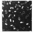
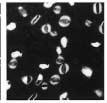
12 Extended Defects: Interstitials Small clusters {311} defects Faulted loops Perfect loops TEM images from Claverie et al. Cowern et al. Cristiano et al.


13 Extended Defects: Interstitial {311} Simulated in DADOS with their actual crystallographic parameters 3D View High B diffusivity 2D Projection {311} defects Interst. Supersat. (Hops)
14 311-defects dissolution Full damage simulation: No +N assumption Defect cross-section automatically given by defect geometry 200 s Simulation 738ºC 1.E+15 interstitials in defects (cm-2) 1.E+14 1.E+13 1.E+12 Experimental: 815ºC 738ºC 705ºC 670ºC Lines: simulation 600 s 1200 s 1.E Anneal time (s) 1800 s Experimental data from Eaglesham et al.

15 Interstitial supersaturation supersaturation Determines dopant diffusivity Interstitial supersaturation 1.E+08 1.E+07 1.E+06 1.E+05 1.E+04 1.E+03 Experimental 600ºC 700ºC 800ºC Lines: 1.E+02 1.E+00 1.E+01 1.E+02 1.E+03 1.E+04 1.E+05 Anneal time (s) Experimental data from Cowern et al.


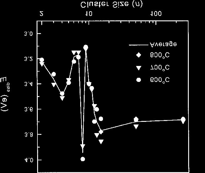
16 Dislocation Loops From Claverie et al. Loop energy < {311} energy if Number of atoms > 345 However, {311} can in fact reach sizes >> 345 DADOS Simulation Therefore, the {311} Loop transformation cannot be based just on minimum configurational energy. {311} Loop: Activation Energy?


17 Extended Defects: Vacancies Big V-clusters are spheroidal (Voids) Energies from Bongiorno et al. (Tight-Binding) But chemical / electrical effects are evident from experiments (Holland et al.): Ge Implant Si Implant Isoelectric As Implant Nearly same atomic Number & Mass P Implant Dopants


18 Extended Defects: Vacancies (II) Si Implant Chemical / electrical effects P Implant No negative Eb at n=7 P Implant Simulation with negative Eb at sizes 7, 11, 15 Si Implant Si Implant


19 Lattice / Non-Lattice KMC Do we need Lattice KMC? Lattice KMC Bongiorno et al. Non-Lattice KMC Attributed to the mobility of small clusters in Lattice- KMC The dominant factor seems to be the energetics. It is not clear the need for Lattice KMC
20 Amorphization / Recrystalization Amorphization:! Massive lattice disorder! Continuum spectrum of time-constants and atomic configurations involved Not amenable to atomic-scale KMC description for device sizes. Implant: 50 KeV, 3.6x10¹⁴ Si/cm2 (Pan et al., APL 1997)
 up to a maximum number per box (MaxStorage) This allows for dynamic anneal between cascades Maintain the correct I-V")

21 Amorphization / Recrystalization Implementation (3D): Small (2nm-side) damage boxes Accumulate Interst. & Vacs. ( disordered pockets ) up to a maximum number per box (MaxStorage) This allows for dynamic anneal between cascades Maintain the correct I-V balance in each box When a box reaches a given damage level becomes an Amorphous region Amorphous regions in contact with the surface or with a crystalline region recrystalize with a given activation energy. Any I-V unbalance is accumulated as the amorphous region shrinks ( dumped onto adjacent amorphous boxes). Top View Cross Sect.

22 Amorphization / Recrystalization KMC Simulation Implant: 50 KeV, 3.6x10¹⁴ Si/cm2 (Pan et al., APL 1997)


23 Amorphization / Recrystalization Simulation 800 C, 60 s (Pan et al., APL 1997) <100> <110> No net I excess within the amorphised layer I,V recombination dissolves {311} and Loops Are V s being held in small, stable clusters, that prevent recombination?
24 Charge Effects: : Implementation! Charge state update static (immobile species) dynamic (mobile species) [I - ] [I o ] = n(x) δi - ni! Electric field(ξ) drift concentration modeled as biased diffusion I - (x) n(x) I -? n i I + (x) x P(+x) P(-x) = exp( q ξ λ ) kt n(x) calculated from charge neutrality approximation no interaction between repulsive species


25 Charge Effects: : Examples! Equilibrium conditions! Non equilibrium Phosphorous in-diffusion
26 ! Inert Surface: I,V Emission Rate = D0*exp(-(Ef+Em)/kT) Recomb. Probability = Recomb. Length Jump Distance! Oxidation: I-supersaturation! Nitridation: V-supersaturation Atomistic KMC can incorporate any currently available injection rate model (from SUPREM, etc)
 Given the Surface concentration calculate")
 of Impurity atoms that arrive at the surface. 2.")
27 Surface: Impurity Atoms! Surface-to-Bulk: (Diffusion from the Surface) Given the Surface concentration calculate the corresponding mobile species emission rate.! Bulk-to-Surface: (Grown-in, Implant, ) 1. Monitor the number (N A ) of Impurity atoms that arrive at the surface. 2. Emit the mobile species at a rate proportional to N A up to the solubility limit.
28 Examples: In Atomistic KMC all mechanisms are operative simultaneously Unforeseen effects can show-up when all mechanisms are included simultaneously 1. Nominally non-amorphising implants (e.g. 40 KeV, cm -2 Si) can still generate small, isolated amorphous regions due to cascade overlapping. 2. Self-diffusion Data (Bracht, Phys. Rev. B 52 (1995) 16542): V parameters (Formation + Migration) The split (Formation, Migration) was chosen such that (together with the V cluster energies from Bongiorno, PRL) V clustering spontaneously generates Voids. Missing mechanisms can lead to missed side-effects.


29 Device Processing Example: A 20-nm NMOSFET (Deleonibus et al., IEEE Electron Dev. Lett., April 2000)

 Anneal: 15 s @ 950 C 15s @ 950 C Anneal CPU time on a 400")
 Deleonibus et al., IEEE Elec. Dev.")
30 Device Processing DADOS Simulation As Implanted 950 C Calculation region: 100x70x50 nm 3 S/D Extension: 3 KeV, As/cm 2 S/D Deep-Implant: 10 KeV, 4x10 14 As/cm 2 (?) Anneal: C 950 C Anneal CPU time on a 400 MHz Pentium-II: 32 min Deep-Implant also simulated (Extension only: 5 min) Deleonibus et al., IEEE Elec. Dev. Lett., April 2000
31 Conclusions Atomistic KMC can handle:! All these mechanisms! Simultaneously! Under highly non-equilibrium conditions! In 3D Atomistic Front-End Process Simulation can advantageously simulate the processing steps of current deep-submicron device technology.
Atomistic simulations on the mobility of di- and tri-interstitials in Si
 Atomistic simulations on the mobility of di- and tri-interstitials in Si related publications (since 2001): Posselt, M., Gao, F., Zwicker, D., Atomistic study of the migration of di- and tri-interstitials
F + Implants in Crystalline Si: The Si Interstitial Contribution
 Mater. Res. Soc. Symp. Proc. Vol. 1070 2008 Materials Research Society 1070-E06-07 F + Implants in Crystalline Si: The Si Interstitial Contribution Pedro Lopez 1, Lourdes Pelaz 1, Ray Duffy 2, P. Meunier-Beillard
Dose loss and segregation of boron and arsenic at the Si/SiO 2 interface by atomistic kinetic Monte Carlo simulations
 Materials Science and Engineering B 124 125 (2005) 392 396 Dose loss and segregation of boron and arsenic at the Si/SiO 2 interface by atomistic kinetic Monte Carlo simulations J.E. Rubio a,, M. Jaraiz
Evolution of fluorine and boron profiles during annealing in crystalline Si
 Evolution of fluorine and boron profiles during annealing in crystalline Si Pedro López a and Lourdes Pelaz Dpto. de Electricidad y Electrónica, Universidad de Valladolid, E.T.S.I. Telecomunicación, 47.011
Carbon in silicon: Modeling of diffusion and clustering mechanisms
 JOURNAL OF APPLIED PHYSIS VOLUME 92, NUMBER 3 1 AUGUST 2002 arbon in silicon: Modeling of diffusion and clustering mechanisms R. Pinacho, a) P. astrillo, M. Jaraiz, I. Martin-Bragado, and J. Barbolla Department
Simple atomistic modeling of dominant B m I n clusters in boron diffusion
 Molecular Simulation, Vol. 31, No. 12, 15 October 2005, 817 824 Simple atomistic modeling of dominant B m I n clusters in boron diffusion J.-H. YOO, C.-O. HWANG, B.-J. KIM and T. WON* Department of Electrical
ION IMPLANTATION - Chapter 8 Basic Concepts
 ION IMPLANTATION - Chapter 8 Basic Concepts Ion implantation is the dominant method of doping used today. In spite of creating enormous lattice damage it is favored because: Large range of doses - 1 11
Linking ab initio Energetics to Experiment: Kinetic Monte Carlo Simulation of Transient Diffusion of B and Si
 UCRL-JC-132824 PREPRINT Linking ab initio Energetics to Experiment: Kinetic Monte Carlo Simulation of Transient Diffusion of B and Si S. Theiss M.J. Cartula T. Diaz de la Rubia M.C. Johnson P.B. Griffin
Physical atomistic kinetic Monte Carlo modeling of Fermi-level effects of species diffusing in Silicon
 Physical atomistic kinetic Monte Carlo modeling of Fermilevel effects of species diffusing in Silicon I. MartinBragado, P. Castrillo, M. Jaraiz, R. Pinacho, J.E. Rubio, and J. Barbolla Department of Electronics,
Abstract We used atomistic simulation tools to correlate experimental transmission
 Journal of Electronic Materials manuscript No. (will be inserted by the editor) Identification of Extended Defect Atomic Configurations in Silicon through Transmission Electron Microscopy Image Simulation
EE 212 FALL ION IMPLANTATION - Chapter 8 Basic Concepts
 EE 212 FALL 1999-00 ION IMPLANTATION - Chapter 8 Basic Concepts Ion implantation is the dominant method of doping used today. In spite of creating enormous lattice damage it is favored because: Large range
Joint ICTP-IAEA Workshop on Physics of Radiation Effect and its Simulation for Non-Metallic Condensed Matter.
 2359-3 Joint ICTP-IAEA Workshop on Physics of Radiation Effect and its Simulation for Non-Metallic Condensed Matter 13-24 August 2012 Electrically active defects in semiconductors induced by radiation
CMOS. Technology Doping Profiles. Simulation of 0.35 Ixm/0.25 INTRODUCTION
 VLSI DESIGN 2001, Vol. 13, Nos. 4, pp. 459-- 463 Reprints available directly from the publisher Photocopying permitted by license only (C) 2001 OPA (Overseas Publishers Association) N.V. Published by license
Dopant and Self-Diffusion in Semiconductors: A Tutorial
 Dopant and Self-Diffusion in Semiconductors: A Tutorial Eugene Haller and Hughes Silvestri MS&E, UCB and LBNL FLCC Tutorial 1/26/04 1 FLCC Outline Motivation Background Fick s Laws Diffusion Mechanisms
Diffusion in Extrinsic Silicon and Silicon Germanium
 1 Diffusion in Extrinsic Silicon and Silicon Germanium SFR Workshop & Review November 14, 2002 Hughes Silvestri, Ian Sharp, Hartmut Bracht, and Eugene Haller Berkeley, CA 2002 GOAL: Diffusion measurements
DIFFUSION - Chapter 7
 DIFFUSION - Chapter 7 Doping profiles determine many short-channel characteristics in MOS devices. Resistance impacts drive current. Scaling implies all lateral and vertical dimensions scale by the same
Electrically active defects in semiconductors induced by radiation
 Electrically active defects in semiconductors induced by radiation Ivana Capan Rudjer Boskovic Institute, Croatia http://www.irb.hr/users/capan Outline Radiation damage Capacitance transient techniques
Ion Implantation ECE723
 Ion Implantation Topic covered: Process and Advantages of Ion Implantation Ion Distribution and Removal of Lattice Damage Simulation of Ion Implantation Range of Implanted Ions Ion Implantation is the
Section 7: Diffusion. Jaeger Chapter 4. EE143 Ali Javey
 Section 7: Diffusion Jaeger Chapter 4 Surface Diffusion: Dopant Sources (a) Gas Source: AsH 3, PH 3, B 2 H 6 (b) Solid Source BN Si BN Si (c) Spin-on-glass SiO 2 +dopant oxide (d) Liquid Source. Fick s
NITROGEN CONTAINING ULTRA THIN SiO 2 FILMS ON Si OBTAINED BY ION IMPLANTATION
 NITROGEN CONTAINING ULTRA THIN SiO 2 FILMS ON Si OBTAINED BY ION IMPLANTATION Sashka Petrova Alexandrova 1, Evgenia Petrova Valcheva 2, Rumen Georgiev Kobilarov 1 1 Department of Applied Physics, Technical
Time accelerated Atomic Kinetic Monte Carlo for radiation damage modelling
 PERFORM 60 FP7 Project Time accelerated Atomic Kinetic Monte Carlo for radiation damage modelling C. Domain, C.S. Becquart, R. Ngayam-Happy EDF R&D Dpt Matériaux & Mécanique des Composants Les Renardieres,
Dopant Diffusion. (1) Predeposition dopant gas. (2) Drive-in Turn off dopant gas. dose control. Doped Si region
 Predeposition dopant gas. (2) Drive-in Turn off dopant gas. dose control. Doped Si region") Dopant Diffusion (1) Predeposition dopant gas dose control SiO Si SiO Doped Si region () Drive-in Turn off dopant gas or seal surface with oxide profile control (junction depth; concentration) SiO SiO
Dopant Diffusion (1) Predeposition dopant gas dose control SiO Si SiO Doped Si region () Drive-in Turn off dopant gas or seal surface with oxide profile control (junction depth; concentration) SiO SiO
Diffusion in Extrinsic Silicon
 1 Diffusion in Extrinsic Silicon SFR Workshop & Review April 17, 2002 Hughes Silvestri, Ian Sharp, Hartmut Bracht, and Eugene Haller Berkeley, CA 2002 GOAL: Diffusion measurements on P doped Si to complete
Fast Monte-Carlo Simulation of Ion Implantation. Binary Collision Approximation Implementation within ATHENA
 Fast Monte-Carlo Simulation of Ion Implantation Binary Collision Approximation Implementation within ATHENA Contents Simulation Challenges for Future Technologies Monte-Carlo Concepts and Models Atomic
Session 5: Solid State Physics. Charge Mobility Drift Diffusion Recombination-Generation
 Session 5: Solid State Physics Charge Mobility Drift Diffusion Recombination-Generation 1 Outline A B C D E F G H I J 2 Mobile Charge Carriers in Semiconductors Three primary types of carrier action occur
Technology computer aided design characterization needs and requirements
 Technology computer aided design characterization needs and requirements Mark E. Law Department of Electrical and Computer Engineering, University of Florida, Gainesville, Florida 32611-6200 Received 20
Atomic configuration of boron pile-up at the Si/SiO 2 interface
 Atomic configuration of boron pile-up at the Si/SiO 2 interface Masayuki Furuhashi, a) Tetsuya Hirose, Hiroshi Tsuji, Masayuki Tachi, and Kenji Taniguchi Department of Electronics and Information Systems,
Modeling the sputter deposition of thin film photovoltaics using long time scale dynamics techniques
 Loughborough University Institutional Repository Modeling the sputter deposition of thin film photovoltaics using long time scale dynamics techniques This item was submitted to Loughborough University's
Vacancy generation during Cu diffusion in GaAs M. Elsayed PhD. Student
 Vacancy generation during Cu diffusion in GaAs M. Elsayed PhD. Student Martin Luther University-FB Physik IV Halle-Wittenberg Outlines Principles of PAS vacancy in Semiconductors and shallow positron traps
2. Point Defects. R. Krause-Rehberg
 R. Krause-Rehberg 2. Point Defects (F-center in acl) 2.1 Introduction 2.2 Classification 2.3 otation 2.4 Examples 2.5 Peculiarities in Semiconductors 2.6 Determination of Structure and Concentration 2.7
Introduction to Semiconductor Physics. Prof.P. Ravindran, Department of Physics, Central University of Tamil Nadu, India
 Introduction to Semiconductor Physics 1 Prof.P. Ravindran, Department of Physics, Central University of Tamil Nadu, India http://folk.uio.no/ravi/cmp2013 Review of Semiconductor Physics Semiconductor fundamentals
EFFECTS OF STOICHIOMETRY ON POINT DEFECTS AND IMPURITIES IN GALLIUM NITRIDE
 EFFECTS OF STOICHIOMETRY ON POINT DEFECTS AND IMPURITIES IN GALLIUM NITRIDE C. G. VAN DE WALLE AND J. E. NORTHRUP Palo Alto Research Center, 3333 Coyote Hill Road, Palo Alto, CA 930, USA E-mail: vandewalle@parc.com
Interaction of ion beams with matter
 Interaction of ion beams with matter Introduction Nuclear and electronic energy loss Radiation damage process Displacements by nuclear stopping Defects by electronic energy loss Defect-free irradiation
First-Passage Kinetic Monte Carlo Algorithm for Complex Reaction-Diffusion Systems
 First-Passage Kinetic Monte Carlo Algorithm for Complex Reaction-Diffusion Systems Aleksandar Donev 1 Lawrence Postdoctoral Fellow Lawrence Livermore National Laboratory In collaboration with: Vasily V.
EFFECT OF PRESSURE ON BORON DIFFUSION IN SILICON Yuechao Zhao 1, Michael J. Aziz 1, Salman Mitha 2, and David Schiferl 3
 EFFECT OF PRESSURE ON BORON DIFFUSION IN SILICON Yuechao Zhao 1, Michael J. Aziz 1, Salman Mitha 2, and David Schiferl 3 1 Division of Engineering and Applied Sciences, Harvard University, Cambridge, MA
Semiconductor physics I. The Crystal Structure of Solids
 Lecture 3 Semiconductor physics I The Crystal Structure of Solids 1 Semiconductor materials Types of solids Space lattices Atomic Bonding Imperfection and doping in SOLIDS 2 Semiconductor Semiconductors
Review of Semiconductor Fundamentals
 ECE 541/ME 541 Microelectronic Fabrication Techniques Review of Semiconductor Fundamentals Zheng Yang (ERF 3017, email: yangzhen@uic.edu) Page 1 Semiconductor A semiconductor is an almost insulating material,
Molecular Dynamics Simulations of Fusion Materials: Challenges and Opportunities (Recent Developments)
") Molecular Dynamics Simulations of Fusion Materials: Challenges and Opportunities (Recent Developments) Fei Gao gaofeium@umich.edu Limitations of MD Time scales Length scales (PBC help a lot) Accuracy of
Molecular Dynamics Simulations of Fusion Materials: Challenges and Opportunities (Recent Developments) Fei Gao gaofeium@umich.edu Limitations of MD Time scales Length scales (PBC help a lot) Accuracy of
A semiconductor is an almost insulating material, in which by contamination (doping) positive or negative charge carriers can be introduced.
 positive or negative charge carriers can be introduced.") Semiconductor A semiconductor is an almost insulating material, in which by contamination (doping) positive or negative charge carriers can be introduced. Page 2 Semiconductor materials Page 3 Energy levels
Semiconductor A semiconductor is an almost insulating material, in which by contamination (doping) positive or negative charge carriers can be introduced. Page 2 Semiconductor materials Page 3 Energy levels
Properties of Error Function erf(z) And Complementary Error Function erfc(z)
 And Complementary Error Function erfc(z)") Properties of Error Function erf(z) And Complementary Error Function erfc(z) z erf (z) π e -y dy erfc (z) 1 - erf (z) erf () erf( ) 1 erf(- ) - 1 erf (z) d erf(z) dz π z for z
Properties of Error Function erf(z) And Complementary Error Function erfc(z) z erf (z) π e -y dy erfc (z) 1 - erf (z) erf () erf( ) 1 erf(- ) - 1 erf (z) d erf(z) dz π z for z
Ion Implantation. alternative to diffusion for the introduction of dopants essentially a physical process, rather than chemical advantages:
 Ion Implantation alternative to diffusion for the introduction of dopants essentially a physical process, rather than chemical advantages: mass separation allows wide varies of dopants dose control: diffusion
Effects of Antimony Near SiO 2 /SiC Interfaces
 Effects of Antimony Near SiO 2 /SiC Interfaces P.M. Mooney, A.F. Basile, and Zenan Jiang Simon Fraser University, Burnaby, BC, V5A1S6, Canada and Yongju Zheng, Tamara Isaacs-Smith Smith, Aaron Modic, and
VLSI Technology Dr. Nandita Dasgupta Department of Electrical Engineering Indian Institute of Technology, Madras
 VLSI Technology Dr. Nandita Dasgupta Department of Electrical Engineering Indian Institute of Technology, Madras Lecture - 20 Ion-implantation systems and damages during implantation So, in our discussion
Luminescence Process
 Luminescence Process The absorption and the emission are related to each other and they are described by two terms which are complex conjugate of each other in the interaction Hamiltonian (H er ). In an
ATOMIC-SCALE THEORY OF RADIATION-INDUCED PHENOMENA
 ATOMIC-SCALE THEORY OF RADIATION-INDUCED PHENOMENA OVERVIEW OF THE LAST FIVE YEARS AND NEW RESULTS Sokrates T. Pantelides Department of Physics and Astronomy, Vanderbilt University, Nashville, TN The theory
Quiz #1 Practice Problem Set
 Name: Student Number: ELEC 3908 Physical Electronics Quiz #1 Practice Problem Set? Minutes January 22, 2016 - No aids except a non-programmable calculator - All questions must be answered - All questions
September 21, 2005, Wednesday
 , Wednesday Doping and diffusion I Faster MOSFET requires shorter channel P + Poly Al Al Motivation Requires shallower source, drain Al P + Poly Al source drain Shorter channel length; yes, but same source
Outlook: Application of Positron Annihilation for defects investigations in thin films. Introduction to Positron Annihilation Methods
 Application of Positron Annihilation for defects investigations in thin films V. Bondarenko, R. Krause-Rehberg Martin-Luther-University Halle-Wittenberg, Halle, Germany Outlook: Introduction to Positron
MODELING DEFECT MEDIATED DOPANT DIFFUSION IN SILICON. by Brian T. Puchala
 MODELING DEFECT MEDIATED DOPANT DIFFUSION IN SILICON by Brian T. Puchala A dissertation submitted in partial fulfillment of the requirements for the degree of Doctor of Philosophy (Materials Science and
Lecture 15 - The pn Junction Diode (I) I-V Characteristics. November 1, 2005
 I-V Characteristics. November 1, 2005") 6.012 - Microelectronic Devices and Circuits - Fall 2005 Lecture 15-1 Lecture 15 - The pn Junction Diode (I) I-V Characteristics November 1, 2005 Contents: 1. pn junction under bias 2. I-V characteristics
6.012 - Microelectronic Devices and Circuits - Fall 2005 Lecture 15-1 Lecture 15 - The pn Junction Diode (I) I-V Characteristics November 1, 2005 Contents: 1. pn junction under bias 2. I-V characteristics
Accelerated ions. ion doping
 30 5. Simulation of Ion Doping of Semiconductors 5.1. Objectives - To give students hand-on experience of numerical simulation of ion doping used for fabrication of semiconductor planar devices. - To familiarize
DIFFUSION IN SOLIDS. IE-114 Materials Science and General Chemistry Lecture-5
 DIFFUSION IN SOLIDS IE-114 Materials Science and General Chemistry Lecture-5 Diffusion The mechanism by which matter is transported through matter. It is related to internal atomic movement. Atomic movement;
E. Chason and S. T. Picraux Sandia National Laboratories, Post Office Box 5800, Albuquerque, New Mexico 87185
 APPLIED PHYSICS REVIEWS Ion beams in silicon processing and characterization E. Chason and S. T. Picraux Sandia National Laboratories, Post Office Box 5800, Albuquerque, New Mexico 87185 J. M. Poate New
Semiconductor-Detectors
 Semiconductor-Detectors 1 Motivation ~ 195: Discovery that pn-- junctions can be used to detect particles. Semiconductor detectors used for energy measurements ( Germanium) Since ~ 3 years: Semiconductor
MIT Amorphous Materials
 MIT 3.071 Amorphous Materials 10: Electrical and Transport Properties Juejun (JJ) Hu 1 After-class reading list Fundamentals of Inorganic Glasses Ch. 14, Ch. 16 Introduction to Glass Science and Technology
KATIHAL FİZİĞİ MNT-510
 KATIHAL FİZİĞİ MNT-510 YARIİLETKENLER Kaynaklar: Katıhal Fiziği, Prof. Dr. Mustafa Dikici, Seçkin Yayıncılık Katıhal Fiziği, Şakir Aydoğan, Nobel Yayıncılık, Physics for Computer Science Students: With
Atomistic simulations of point defect diffusion in Si and SiGe
 Atomistic simulations of point defect diffusion in Si and SiGe P. Pochet, D. Caliste, K. Rushchanskii, F. Lançon & T. Deutsch CEA UJF INAC Institute for Nanoscience and Cryogenics Partially founded by
The effect of point defects in zircon
 aterials for nuclear waste immobilization: The effect of point defects in zircon iguel Pruneda Department of Earth Sciences University of Centre for Ceramic Immobilisation Radiation damage process α-decay
Identification of Getter Defects in high-energy self-implanted Silicon at Rp/2
 Identification of Getter Defects in high-energy self-implanted Silicon at Rp R. Krause-Rehberg 1, F. Börner 1, F. Redmann 1, J. Gebauer 1, R. Kögler 2, R. Kliemann 2, W. Skorupa 2, W. Egger 3, G. Kögel
3.1 Introduction to Semiconductors. Y. Baghzouz ECE Department UNLV
 3.1 Introduction to Semiconductors Y. Baghzouz ECE Department UNLV Introduction In this lecture, we will cover the basic aspects of semiconductor materials, and the physical mechanisms which are at the
Chap. 11 Semiconductor Diodes
 Chap. 11 Semiconductor Diodes Semiconductor diodes provide the best resolution for energy measurements, silicon based devices are generally used for charged-particles, germanium for photons. Scintillators
Ion implantation Campbell, Chapter 5
 Ion implantation Campbell, Chapter 5 background why ion implant? elastic collisions nuclear and electronic stopping ion ranges: projected and lateral channeling ion-induced damage and amorphization basic
Lab1. Resolution and Throughput of Ion Beam Lithography.
 1 ENS/PHY463 Lab1. Resolution and Throughput of Ion Beam Lithography. (SRIM 2008/2013 computer simulation) Objective The objective of this laboratory work is to evaluate the exposure depth, resolution,
Abstract We combined several atomistic techniques to identify the structure of
 Journal of Electronic Materials manuscript No. (will be inserted by the editor) W and X photoluminescence centers in crystalline Si: chasing candidates at atomic level through multiscale simulations María
Lecture 1. OUTLINE Basic Semiconductor Physics. Reading: Chapter 2.1. Semiconductors Intrinsic (undoped) silicon Doping Carrier concentrations
 silicon Doping Carrier concentrations") Lecture 1 OUTLINE Basic Semiconductor Physics Semiconductors Intrinsic (undoped) silicon Doping Carrier concentrations Reading: Chapter 2.1 EE105 Fall 2007 Lecture 1, Slide 1 What is a Semiconductor? Low
Lecture 1 OUTLINE Basic Semiconductor Physics Semiconductors Intrinsic (undoped) silicon Doping Carrier concentrations Reading: Chapter 2.1 EE105 Fall 2007 Lecture 1, Slide 1 What is a Semiconductor? Low
ISSUES TO ADDRESS...
 Chapter 12: Electrical Properties School of Mechanical Engineering Choi, Hae-Jin Materials Science - Prof. Choi, Hae-Jin Chapter 12-1 ISSUES TO ADDRESS... How are electrical conductance and resistance
Three-Dimensional Silicon-Germanium Nanostructures for Light Emitters and On-Chip Optical. Interconnects
 Three-Dimensional Silicon-Germanium Nanostructures for Light Emitters and On-Chip Optical eptember 2011 Interconnects Leonid Tsybeskov Department of Electrical and Computer Engineering New Jersey Institute
Feature-level Compensation & Control. Process Integration September 15, A UC Discovery Project
 Feature-level Compensation & Control Process Integration September 15, 2005 A UC Discovery Project Current Milestones Si/Ge-on-insulator and Strained Si-on-insulator Substrate Engineering (M28 YII.13)
in Si by means of Positron Annihilation
 Investigation of the Rp/2 /2-effect in Si by means of Positron Annihilation R. Krause-Rehberg, F. Börner, F. Redmann Universität Halle Martin-Luther-Universität R. Kögler, W. Skorupa Forschungszentrum
Calculating Band Structure
 Calculating Band Structure Nearly free electron Assume plane wave solution for electrons Weak potential V(x) Brillouin zone edge Tight binding method Electrons in local atomic states (bound states) Interatomic
Multiscale modelling of D trapping in W
 CMS Multiscale modelling of D trapping in W Kalle Heinola, Tommy Ahlgren and Kai Nordlund Department of Physics and Helsinki Institute of Physics University of Helsinki, Finland Contents Background Plasma-wall
Chapter 12: Electrical Properties. RA l
 Charge carriers and conduction: Chapter 12: Electrical Properties Charge carriers include all species capable of transporting electrical charge, including electrons, ions, and electron holes. The latter
Surface analysis techniques
 Experimental methods in physics Surface analysis techniques 3. Ion probes Elemental and molecular analysis Jean-Marc Bonard Academic year 10-11 3. Elemental and molecular analysis 3.1.!Secondary ion mass
Semiconductor Device Physics
 1 Semiconductor Device Physics Lecture 3 http://zitompul.wordpress.com 2 0 1 3 Semiconductor Device Physics 2 Three primary types of carrier action occur inside a semiconductor: Drift: charged particle
Processing of Semiconducting Materials Prof. Pallab Banerji Department of Metallurgy and Material Science Indian Institute of Technology, Kharagpur
 Processing of Semiconducting Materials Prof. Pallab Banerji Department of Metallurgy and Material Science Indian Institute of Technology, Kharagpur Lecture - 9 Diffusion and Ion Implantation III In my
Minimal Update of Solid State Physics
 Minimal Update of Solid State Physics It is expected that participants are acquainted with basics of solid state physics. Therefore here we will refresh only those aspects, which are absolutely necessary
collisions of electrons. In semiconductor, in certain temperature ranges the conductivity increases rapidly by increasing temperature
 1.9. Temperature Dependence of Semiconductor Conductivity Such dependence is one most important in semiconductor. In metals, Conductivity decreases by increasing temperature due to greater frequency of
Experience with Moving from Dpa to Changes in Materials Properties
 Experience with Moving from Dpa to Changes in Materials Properties Meimei Li, Argonne National Laboratory N. V. Mokhov, Fermilab 46 th ICFA Advanced Beam Dynamics Workshop Sept. 27 Oct. 1, 2010 Morschach,
Quantum and Non-local Transport Models in Crosslight Device Simulators. Copyright 2008 Crosslight Software Inc.
 Quantum and Non-local Transport Models in Crosslight Device Simulators Copyright 2008 Crosslight Software Inc. 1 Introduction Quantization effects Content Self-consistent charge-potential profile. Space
Metal Semiconductor Contacts
 Metal Semiconductor Contacts The investigation of rectification in metal-semiconductor contacts was first described by Braun [33-35], who discovered in 1874 the asymmetric nature of electrical conduction
ATOMISTIC MODELING OF BORON ACTIVATION AND DIFFUSION IN STRAINED SIGE
 ATOMISTIC MODELING OF BORON ACTIVATION AND DIFFUSION IN STRAINED SIGE Scott T. Dunham,, Jakyoung Song, and Chihak Ahn Dept. of Electrical Engineering, Dept. of Physics University of Washington, Box 35500,
Lab 3. Ion Implantation
 1 Lab 3. Ion Implantation (SRIM 2008/2013 computer simulation) 1. Objectives - To give students hand-on experience of numerical simulation of ion doping used for fabrication of semiconductor nanodevices.
Modelling of radiation damage in tungsten including He production
 Modelling of radiation damage in tungsten including He production C.S. Becquart 1, C. Domain 2 A. De Backer 1 M.F. Barthe 3 M. Hou 4, C. Ortiz 5 1 Unité Matériaux Et Techniques, UMET, UMR 8207, Villeneuve
Solid State Physics SEMICONDUCTORS - IV. Lecture 25. A.H. Harker. Physics and Astronomy UCL
 Solid State Physics SEMICONDUCTORS - IV Lecture 25 A.H. Harker Physics and Astronomy UCL 9.9 Carrier diffusion and recombination Suppose we have a p-type semiconductor, i.e. n h >> n e. (1) Create a local
Kinetic lattice Monte Carlo simulations of diffusion processes in Si and SiGe alloys
 Kinetic lattice Monte Carlo simulations of diffusion processes in Si and SiGe alloys, Scott Dunham Department of Electrical Engineering Multiscale Modeling Hierarchy Configuration energies and transition
Effect of the Si SiO2 Interface on Diffusion in SiO2
 Vol. 26, No. 5, pp. 249254, 2005 Si SiO2 SiSiO2 CREST-JST 2238522 3141 NTT 2430198 31 3058571 111 2004 11 1 Effect of the SiSiO2 Interface on Diffusion in SiO2 Shigeto FUKATSU, KoheiM.ITOH, Masashi UEMATSU,
Semiconductor Physics Problems 2015
 Semiconductor Physics Problems 2015 Page and figure numbers refer to Semiconductor Devices Physics and Technology, 3rd edition, by SM Sze and M-K Lee 1. The purest semiconductor crystals it is possible
Improvement of depth resolution of VEPAS by a sputtering technique
 Martin Luther University Halle Improvement of depth resolution of VEPAS by a sputtering technique R. Krause Rehberg, M. John, R. Böttger, W. Anwand and A. Wagner Martin Luther University Halle & HZDR Dresden
Luminescence basics. Slide # 1
 Luminescence basics Types of luminescence Cathodoluminescence: Luminescence due to recombination of EHPs created by energetic electrons. Example: CL mapping system Photoluminescence: Luminescence due to
MOS CAPACITOR AND MOSFET
 EE336 Semiconductor Devices 1 MOS CAPACITOR AND MOSFET Dr. Mohammed M. Farag Ideal MOS Capacitor Semiconductor Devices Physics and Technology Chapter 5 EE336 Semiconductor Devices 2 MOS Capacitor Structure
Semiconductor Physical Electronics
 Semiconductor Physical Electronics Sheng S. Li Department of Electrical Engineering University of Florida Gainesville, Florida Plenum Press New York and London Contents CHAPTER 1. Classification of Solids
Morphological evolution of single-crystal ultrathin solid films
 Western Kentucky University From the SelectedWorks of Mikhail Khenner March 29, 2010 Morphological evolution of single-crystal ultrathin solid films Mikhail Khenner, Western Kentucky University Available
The peculiarities of formation of implanted atom concentration beyond the ion range. V.I. Sugakov Institute for Nuclear Research, Kyiv, Ukraine
 The peculiarities of formation of implanted atom concentration beyond the ion range V.I. Sugakov Institute for Nuclear Research, Kyiv, Ukraine Range He in Si, 10 kev Defects E z p (10 100) kev (0.01 0.1)
Theoretical Studies of Self-Diffusion and Dopant Clustering in Semiconductors
 phys. stat. sol. (b) zzz, No. z, zzz zzz (2002) Theoretical Studies of Self-Diffusion and Dopant Clustering in Semiconductors B.P. Uberuaga )(a), G. Henkelman (b), H. Jónsson (b) (c), S.T. Dunham (d),
Introduction into Positron Annihilation
 Introduction into Positron Annihilation Introduction (How to get positrons? What is special about positron annihilation?) The methods of positron annihilation (positron lifetime, Doppler broadening, ACAR...)
n N D n p = n i p N A
 Summary of electron and hole concentration in semiconductors Intrinsic semiconductor: E G n kt i = pi = N e 2 0 Donor-doped semiconductor: n N D where N D is the concentration of donor impurity Acceptor-doped
Defects in Crystals. Image borrowed from who got it from Davis & Reynolds 1996.
 Defects in Crystals Image borrowed from http://comp.uark.edu/~pjansma/geol3513_25_defmechs1_04.ppt who got it from Davis & Reynolds 1996. It's easy to think of real crystals as having these ideal structures.
Kinetic Monte Carlo: from transition probabilities to transition rates
 Kinetic Monte Carlo: from transition probabilities to transition rates With MD we can only reproduce the dynamics of the system for 100 ns. Slow thermallyactivated processes, such as diffusion, cannot
Recombination: Depletion. Auger, and Tunnelling
 Recombination: Depletion Region, Bulk, Radiative, Auger, and Tunnelling Ch 140 Lecture Notes #13 Prepared by David Gleason We assume: Review of Depletion Region Recombination Flat Quantum Fermi Levels
Cherry-Pit Structures in Binary Immiscible Alloy Under Ion Irradiation
 Cherry-Pit Structures in Binary Immiscible Alloy Under Ion Irradiation Shipeng Shu, Kenneth Tussey May 8, 2011 Abstract We study an special microstructure (matrix atom riched small clusters inside the