Vacancy generation during Cu diffusion in GaAs M. Elsayed PhD. Student
|
|
|
- Adrian Scott
- 5 years ago
- Views:
Transcription

1 Vacancy generation during Cu diffusion in GaAs M. Elsayed PhD. Student Martin Luther University-FB Physik IV Halle-Wittenberg
2 Outlines Principles of PAS vacancy in Semiconductors and shallow positron traps Atomic diffusion mechanisms Observation of vacancies during Cu diffusion in GaAs Conclusion 2


3 Principles of PAS positrons: thermalize diffuse being trapped When trapped in vacancies: Lifetime increases due to smaller electron density in open volume 3


4 Principles of PAS 4
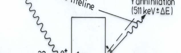
5 Principles of PAS Positron lifetime is measured as time difference between 1.27 MeV quantum and MeV quantum PM=photomultiplier, SCA=single channel analyzer (constant fraction type), TAC=time to amplitude converter, MCA= multi channel analyzer 5
6 Principles of PAS Measurement of Doppler Broadening electron momentum in propagation direction of 511 kev γ-ray leads to Doppler broadening of annihilation line can be detected by conventional energy-dispersive Ge detectors and standard electronics 6
7 Principles of PAS Line Shape Parameters Valance annihilation (Shape) parameter Core annihilation (Wing) parameter Both S and W are sensitive to the concentration and defect type W is sensitive to chemical surrounding of the annihilation site, due to high momentum of core electrons participating in annihilation CDBS 2 γ-detectors (germanium) simultaneously better energy resolution and reduced background 7
8 Vacancies in a semiconductor Vacancies in a semiconductor may be charged For a negative vacancy: Coulomb potential is rather extended but weak it supports trapping only at low temperatures at higher temperatures: detrapping dominates and vacancy behaves like a vacancy in a metal or a neutral vacancy Positive vacancies repel positrons 8
9 Vacancies in a semiconductor Positron trapping by negative vacancies trapping process can be described quantitatively by trapping model Coulomb potential leads to Rydberg states from there: positrons may reescape by thermal stimulation once in the deep state: positron is captured until annihilation detrapping is strongly temperature dependent δ R * 3/2 K R m k BT ER = exp 2 ρv 2πh k BT Manninen, Nieminen,
10 Vacancies in a semiconductor Negative vacancies show temperature-dependent positron trapping dependence of positron trapping on temperature is rather complex κ = ϑρκ T R V R ο 3/2 1/2 * mk B E R ϑρ R V + κr T exp ο 2 2π h k BT positron trapping in negatively charged Ga vacancies in SI-GaAs low temperature: ~ T -1/2 due to limitation of diffusion in Rydberg states higher T: stronger temperature dependence due to thermal detrapping from Rydberg state Le Berre et al.,
11 Shallow positron traps at low T: negatively charged defects without open volume may trap positrons and trapping is based on the capture of positron in Rydberg states shallow refer to small positron binding energy acceptor-typeimpurities, p negative antisite defects annihilation parameters close to bulk parameters thermally stimulated detrapping can be described by: 3/2 * κ mkt B E st δ = exp 2 ρst 2πh k BT Saarrinen et al.,
12 Atomic diffusion mechanisms 1- Diffusion without involvement of native point defect Interstitially dissolved impurity atoms diffuse by jumping between interstitial sites Examples: diffusion of Li, Fe and Cu in Si. Also Oxygen diffuse among interstitial sites with so low diffusivity 12
13 Atomic diffusion mechanisms 2. Simple Vacancy Exchange & Interstitialcy Mechanisms In a simple vacancy exchange mechanism, substitutional atom jumps into a neighbor vacancy on the lattice D C v s eq v In interstitialcy Mechanism (interstitial), the substitutional atom is first replaced by a self-interstitial and pushed into an interstitial position, it pushes out one of the neighbor atom in the lattice D C I s eq I 13
 remains for many steps A A +II i is qualitatively different from vacancy exchange")
14 Atomic diffusion mechanisms 3- Interstitial- Substitutional Mechanism 3.1- Kick-out mechanism 3.2- Frank Turnbull mechanism closely related to interstitialcy diffusion mechanism foreign atom (interstitial) remains for many steps A A +II i is qualitatively different from vacancy exchange mechanism D 1/C A+V s i s v s 4- Recombination-Enhanced diffusion A eq v Thermally activated diffusion of defects may beenhanced by the transfer of energy associated with the recombination of electrons and holes into the vibrational modes of defects and their surrounding C>C eq induced by optical excitation or particle irradiation 14
15 Observation of vacancies during Cu diffusion in GaAs Copper is an unintentional impurity in most semiconductors Cu diffuses rapidly already at low temperatures GaAs: diffusion coefficient D = cm 2 s -1 at 500 C [1] Cu diffuses very fast by interstitial diffusion (kick-out process) [2] The solubility between cm -3 (500 C) and cm -3 (1100 C) [1] Cu Ga is a double acceptor work: comprehensive positron annihilation study of GaAs after Cu in-diffusion Experimental: 0.5 mm samples covered by 30 nm Cu, annealed at 1100 o C under different P As ( bar), quenched in RT water and subject to isochronal annealing [1] R.N. Hall and J.H. Racette, J. Appl. Phys. 35 (1964) 379. [2] F.C. Frank and D. Turnball, Phys. Rev. 104 (1956) 617. RK R 15
16 GaAs:Cu as-quenched and for annealing up to 550 K almost no change in τ av. Up to 800 K, τ av increase strongly to (ps) 290 ps- detected vacancy must be 270 lager than V Ga. Decrease of τ av at low T, shallow av positron traps (Cu Ga ). annealing > 800 K, the vacancy signal disappear. Average posit tron lifetime as-quenched K 600 K 650 K K 750 K 800 K K Measurement temperature (K) 16
17 GaAs:Cu τ d is much higher than that for 450 monovacancies ( ps) from τ d open volume increases during 300 annealing efect-related lifetime (ps) D 600 τ τ 2 τ 3 this explained by trapping of positron 290 at small microvoids. τ 3 reach the value of 600 ps corresponding to vacancy clusters with n > 10 [3]. ifetime (ps) Average pos. l measurement temperature: t 466 K [3] T.E.M. Staab et. el. Physica B (1999) Annealing temperature (K) 17
18 GaAs:Cu K d 1 τ τ av b = μ C = τ b τd τav μ= s -1 at RT n increase from 1 at 466 K up to 4 vacancies at 700 K [3] Defect conce entration (cm -3 ) Nu umber of vacanc cies x x x x x10 3.0x Annealing temperature (K) [3]TEM T.E.M. Staab et. el. Physica B (1999)
19 GaAs:Cu 260 SI GaAs sample was not treated with Cu and annealed at 1100 o Cunder 0.2 bar P As As-quenched sample shows a higher τ av. In contrary, GaAs samples after Cu indiffusion, almost no change of τ av in the as-quenched state Average positro on lifitime (ps) as-grown 700 K as-quenched 750 K 600 K 850 K Measurement temperature (K) 19
20 GaAs:Cu 400 Vacancy + shallow traps [V] and P As exhibit reciprocal dependence τ d = 293 ± 10 ps τ d = 254 and 262 ps in Te and Si doped GaAs τ d = 330 ps for V Ga -V As Defect-re elated lifetime (p ps) Average life etime (ps) p As (bar): reference Measurement temperature (K) 20
21 GaAs:Cu P As vacancy concentration dependence - concentration were determined at RT with µ= s -1 - different slopes for GaAs:Si and SI GaAs - different vacancy sublattices Thermodynamic reactions V Ga : V As : 1/4As As +V gas 4 As Ga [ ] 1/4 V = K P As Ga VGa As V +1/4As gas As As 4-1/4 [ V ] = K P As VAs As Vacanc cy concentration n (cm -3 ) SI-GaAs GaAs:Si Copper Arsenic pressure (bar) Fit: ln[v]= nx ln(p As ) - GaAs:Si n= 0.25 ± SI GaAs n= ±
22 GaAs:Cu for e + annihilation with Cu core e -,the ratio of high momentum part > 1 and presence of Cu in neighbor of e + trap seen as such characteristic increase in intensityi of e - e + momentum distribution no sign of Cu in vicinity of the 1.0 detected vacancies in annealed GaAs Cu is not constitute of the defect complex V As -like defect should be related to a native defect-complex Ratio to the bulk Ga aas SI GaAs after Cu-indiffusion SI GaAs annealed at 1100 o C under P As =0.2 bar Cu p L (10-3 m 0 c) 22
23 Conclusions Positron annihilation is a sensitive tool for investigation of vacancy-like defects and their charge states in semiconductors Vacancy-like defect and shallow traps were observed from the thermodynamics, defect complex contains V As V As is positively charged, vacancy complex containing an As vacancy was assumed CDBS, Cu is not a constituent of the defect complex vacancy complex represents a native defect complex but thestructuret t can not beexactly recognized df from e + annihilation parameters alone 23
24 Vielen Dank fuer Ihre Aufmerksamkeit 24
Study of semiconductors with positrons. Outlook:
 Study of semiconductors with positrons V. Bondarenko, R. Krause-Rehberg Martin-Luther-University Halle-Wittenberg, Halle, Germany Introduction Positron trapping into defects Methods of positron annihilation
Introduction into Positron Annihilation
 Introduction into Positron Annihilation Introduction (How to get positrons? What is special about positron annihilation?) The methods of positron annihilation (positron lifetime, Doppler broadening, ACAR...)
Defect chemistry in GaAs studied by two-zone annealings under defined As vapor pressure. Outlook:
 Defect chemistry in studied by two-zone annealings under defined vapor pressure V. Bondarenko 1, R. Krause-Rehberg 1, J. Gebauer 2, F. Redmann 1 1 Martin-Luther-University Halle-Wittenberg, Halle, Germany
Basics and Means of Positron Annihilation
 Basics and Means of Positron Annihilation Positron history Means of positron annihilation positron lifetime spectroscopy angular correlation Doppler-broadening spectroscopy Near-surface positron experiments:
Vacancy-like defects in SI GaAs: post-growth treatment
 Vacancy-like defects in SI : post-growth treatment V. Bondarenko, R. Krause-Rehberg Martin-Luther-University Halle-Wittenberg, Halle, Germany B. Gruendig-Wendrock, J.R. Niklas TU Bergakademie Freiberg,
Outlook: Application of Positron Annihilation for defects investigations in thin films. Introduction to Positron Annihilation Methods
 Application of Positron Annihilation for defects investigations in thin films V. Bondarenko, R. Krause-Rehberg Martin-Luther-University Halle-Wittenberg, Halle, Germany Outlook: Introduction to Positron
The appearance of vacancies during Cu and Zn diffusion in III-V compound semiconductors
 The appearance of vacancies during Cu and Zn diffusion in III-V compound semiconductors Dissertation zur Erlangung des akademischen Grades Dr. rerum naturalium (Dr. rer. nat.) vorgelegt der Mathematisch-Naturwissenschaftlich-Technischen
Positron Annihilation Spectroscopy - A non-destructive method for material testing -
 Maik Butterling Institute of Radiation Physics http://www.hzdr.de Positron Annihilation Spectroscopy - A non-destructive method for material testing - Maik Butterling Positron Annihilation Spectroscopy
2. Point Defects. R. Krause-Rehberg
 R. Krause-Rehberg 2. Point Defects (F-center in NaCl) 2.1 Introduction 2.2 Classification 2.3 Notation 2.4 Examples 2.5 Peculiarities in Semiconductors 2.6 Determination of Structure and Concentration
in Si by means of Positron Annihilation
 Investigation of the Rp/2 /2-effect in Si by means of Positron Annihilation R. Krause-Rehberg, F. Börner, F. Redmann Universität Halle Martin-Luther-Universität R. Kögler, W. Skorupa Forschungszentrum
Material Science using Positron Annihilation
 Material Science using Positron Annihilation R. Krause-Rehberg Universität Halle, Inst. für Physik 9.3.2018 Some historical remarks Techniques of Positron Annihilation Study of Defects in Semiconductors
Identification of the 0.95 ev luminescence band in n-type GaAs:Si
 INSTITUTE OF PHYSICS PUBLISHING JOURNAL OF PHYSICS: CONDENSED MATTER J. Phys.: Condens. Matter 15 (2003) 1 7 PII: S0953-8984(03)66937-7 Identification of the 0.95 ev luminescence band in n-type GaAs:Si
Positron Annihilation Spectroscopy on Defects in Semiconductors
 Positron Annihilation Spectroscopy on Defects in Semiconductors R. Krause-Rehberg Universität Halle, Inst. für Physik Some historical remarks Techniques of Positron Annihilation Study of Defects in Semiconductors
Investigation of SiC by Positrons
 nd/march/000/erlangen Investigation of SiC by Positrons Atsuo KAWASUSO Martin-Luther-Universität Halle-Wittenberg (Humboldt Research Fellow) Japan Atomic Energy Research Institute Takasaki Establishment
Positron Annihilation in Materials Science
 Positron Annihilation in Materials Science R. Krause-Rehberg Universität Halle, Inst. für Physik History Techniques of Positron Annihilation Defects in Semiconductors User-dedicated Positron Facilities
Photoionization of the silicon divacancy studied by positron-annihilation spectroscopy
 PHYSICAL REVIEW B VOLUME 57, NUMBER 20 15 MAY 1998-II Photoionization of the silicon divacancy studied by positron-annihilation spectroscopy H. Kauppinen* and C. Corbel Institut National des Sciences et
R. Krause-Rehberg. Martin-Luther-Universität Halle-Wittenberg. Positron Lifetime / Doppler Broadening / Angular Correlation / AMOC
 Experimental Techniques of Positron Annihilation and the pulsed Positron Source EPOS R. Krause-Rehberg -Wittenberg Techniques of Positron Annihilation Positron Sources Positron Lifetime / Doppler Broadening
Positron Annihilation Spectroscopy
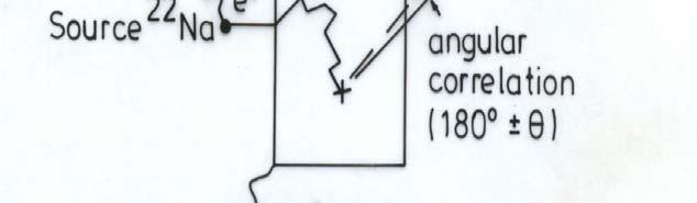
 Positron Annihilation Spectroscopy (1) Angular Correlation θ N x, y = p x, y m C θ γ-ray (511keV ± E) 0 (2) Doppler Broadening Cp E = z 2 θ N p ~100µm 22 Na (e + Source) e - e + ~ 10-12 s Sample γ-ray
DEVELOPMENT OF A NEW POSITRON LIFETIME SPECTROSCOPY TECHNIQUE FOR DEFECT CHARACTERIZATION IN THICK MATERIALS
 Copyright JCPDS - International Centre for Diffraction Data 2004, Advances in X-ray Analysis, Volume 47. 59 DEVELOPMENT OF A NEW POSITRON LIFETIME SPECTROSCOPY TECHNIQUE FOR DEFECT CHARACTERIZATION IN
POSITRON AND POSITRONIUM INTERACTIONS WITH CONDENSED MATTER. Paul Coleman University of Bath
 POSITRON AND POSITRONIUM INTERACTIONS WITH CONDENSED MATTER Paul Coleman University of Bath THE FATE OF POSITRONS IN CONDENSED MATTER POSITRON-SURFACE INTERACTIONS positron backscattering BACKSCATTERED
2. Point Defects. R. Krause-Rehberg
 R. Krause-Rehberg 2. Point Defects (F-center in acl) 2.1 Introduction 2.2 Classification 2.3 otation 2.4 Examples 2.5 Peculiarities in Semiconductors 2.6 Determination of Structure and Concentration 2.7
Unmanageable Defects in Proton- Irradiated Silicon: a Factual Outlook for Positron Probing N. Yu. Arutyunov 1,2, M. Elsayed 1, R.
 Unmanageable Defects in Proton- Irradiated Silicon: a Factual Outlook for Positron Probing N. Yu. Arutyunov 1,2, M. Elsayed 1, R. Krause-Rehberg 1 1 Department of Physics, Martin Luther University, 06120
Identification of Getter Defects in high-energy self-implanted Silicon at Rp/2
 Identification of Getter Defects in high-energy self-implanted Silicon at Rp R. Krause-Rehberg 1, F. Börner 1, F. Redmann 1, J. Gebauer 1, R. Kögler 2, R. Kliemann 2, W. Skorupa 2, W. Egger 3, G. Kögel
Research Center Dresden Rossendorf
 News of the EPOS Project at the ELBE Radiation Source in the Research Center Dresden Rossendorf EPOS-Team & R. Krause-Rehberg Extended Concept of EPOS Progress of the mono-energetic Positron Beam (MePS)
characterization in solids
 Electrical methods for the defect characterization in solids 1. Electrical residual resistivity in metals 2. Hall effect in semiconductors 3. Deep Level Transient Spectroscopy - DLTS Electrical conductivity
Session 5: Solid State Physics. Charge Mobility Drift Diffusion Recombination-Generation
 Session 5: Solid State Physics Charge Mobility Drift Diffusion Recombination-Generation 1 Outline A B C D E F G H I J 2 Mobile Charge Carriers in Semiconductors Three primary types of carrier action occur
Application of positrons in materials research
 Application of positrons in materials research Trapping of positrons at vacancy defects Using positrons, one can get defect information. R. Krause-Rehberg and H. S. Leipner, Positron annihilation in Semiconductors,
EFFECTS OF STOICHIOMETRY ON POINT DEFECTS AND IMPURITIES IN GALLIUM NITRIDE
 EFFECTS OF STOICHIOMETRY ON POINT DEFECTS AND IMPURITIES IN GALLIUM NITRIDE C. G. VAN DE WALLE AND J. E. NORTHRUP Palo Alto Research Center, 3333 Coyote Hill Road, Palo Alto, CA 930, USA E-mail: vandewalle@parc.com
Minimal Update of Solid State Physics
 Minimal Update of Solid State Physics It is expected that participants are acquainted with basics of solid state physics. Therefore here we will refresh only those aspects, which are absolutely necessary
New Concept of EPOS Progress of the Mono-energetic Positron Beam (MePS) Gamma-induced Positron Spectroscopy (GiPS)
 Gamma-induced Positron Spectroscopy (GiPS)") Progress of the EPOS Project: Gamma Induced Positron Spectroscopy (GiPS) R. Krause-Rehberg 1,*,W.Anwand 2,G.Brauer 2, M. Butterling 1,T.Cowan 2,M. Jungmann 1, A. Krille 1, R. Schwengner 2, A. Wagner 2
Progress of the EPOS Project: Gamma Induced Positron Spectroscopy (GiPS) R. Krause-Rehberg 1,*,W.Anwand 2,G.Brauer 2, M. Butterling 1,T.Cowan 2,M. Jungmann 1, A. Krille 1, R. Schwengner 2, A. Wagner 2
Lecture 7: Extrinsic semiconductors - Fermi level
 Lecture 7: Extrinsic semiconductors - Fermi level Contents 1 Dopant materials 1 2 E F in extrinsic semiconductors 5 3 Temperature dependence of carrier concentration 6 3.1 Low temperature regime (T < T
Semiconductor physics I. The Crystal Structure of Solids
 Lecture 3 Semiconductor physics I The Crystal Structure of Solids 1 Semiconductor materials Types of solids Space lattices Atomic Bonding Imperfection and doping in SOLIDS 2 Semiconductor Semiconductors
Tuomisto, Filip; Ranki, V.; Look, D.C.; Farlow, G.C. Introduction and recovery of Ga and N sublattice defects in electron-irradiated GaN
 Powered by TCPDF (www.tcpdf.org) This is an electronic reprint of the original article. This reprint may differ from the original in pagination and typographic detail. Tuomisto, Filip; Ranki, V.; Look,
Joint ICTP-IAEA Workshop on Physics of Radiation Effect and its Simulation for Non-Metallic Condensed Matter.
 2359-3 Joint ICTP-IAEA Workshop on Physics of Radiation Effect and its Simulation for Non-Metallic Condensed Matter 13-24 August 2012 Electrically active defects in semiconductors induced by radiation
Electrons, Holes, and Defect ionization
 Electrons, Holes, and Defect ionization The process of forming intrinsic electron-hole pairs is excitation a cross the band gap ( formation energy ). intrinsic electronic reaction : null e + h When electrons
Defect structure and oxygen diffusion in PZT ceramics
 Defect structure and oxygen diffusion in PZT ceramics Adam Georg Balogh Institute of Materials Science Technische Universität Darmstadt A. G. Balogh Folie 1 Introduction Ferroelectrics are of great technical
2. Thermodynamics of native point defects in GaAs
 2. Thermodynamics o native point deects in The totality o point deects in a crystal comprise those existing in a perectly chemically pure crystal, so called intrinsic deects, and those associated with
Multiscale modelling of D trapping in W
 CMS Multiscale modelling of D trapping in W Kalle Heinola, Tommy Ahlgren and Kai Nordlund Department of Physics and Helsinki Institute of Physics University of Helsinki, Finland Contents Background Plasma-wall
Review of Optical Properties of Materials
 Review of Optical Properties of Materials Review of optics Absorption in semiconductors: qualitative discussion Derivation of Optical Absorption Coefficient in Direct Semiconductors Photons When dealing
Diffusion in Extrinsic Silicon and Silicon Germanium
 1 Diffusion in Extrinsic Silicon and Silicon Germanium SFR Workshop & Review November 14, 2002 Hughes Silvestri, Ian Sharp, Hartmut Bracht, and Eugene Haller Berkeley, CA 2002 GOAL: Diffusion measurements
Thermally Activated Processes
 General Description of Activated Process: 1 Diffusion: 2 Diffusion: Temperature Plays a significant role in diffusion Temperature is not the driving force. Remember: DRIVING FORCE GRADIENT of a FIELD VARIALE
Characterization of native point defects in GaN by positron annihilation spectroscopy
 1 Characterizat of native point defects in GaN by positron annihilat spectroscopy K. Saarinen Laboratory of Physics, Helsinki University of Technology, P. O. Box 1100, FIN-02015 HUT, Finland (in: III-V
Section 7: Diffusion. Jaeger Chapter 4. EE143 Ali Javey
 Section 7: Diffusion Jaeger Chapter 4 Surface Diffusion: Dopant Sources (a) Gas Source: AsH 3, PH 3, B 2 H 6 (b) Solid Source BN Si BN Si (c) Spin-on-glass SiO 2 +dopant oxide (d) Liquid Source. Fick s
collisions of electrons. In semiconductor, in certain temperature ranges the conductivity increases rapidly by increasing temperature
 1.9. Temperature Dependence of Semiconductor Conductivity Such dependence is one most important in semiconductor. In metals, Conductivity decreases by increasing temperature due to greater frequency of
Atomistic Front-End Process Modeling
 Atomistic Front-End Process Modeling A Powerful Tool for Deep-Submicron Device Fabrication SISPAD 2001, Athens Martin Jaraiz University of Valladolid, Spain Thanks to: P. Castrillo (U. Valladolid) R. Pinacho
Dopant and Self-Diffusion in Semiconductors: A Tutorial
 Dopant and Self-Diffusion in Semiconductors: A Tutorial Eugene Haller and Hughes Silvestri MS&E, UCB and LBNL FLCC Tutorial 1/26/04 1 FLCC Outline Motivation Background Fick s Laws Diffusion Mechanisms
The intense, pulsed positron source EPOS at the Research Centre Dresden-Rossendorf
 The intense, pulsed positron source EPOS at the Research Centre Dresden-Rossendorf The EPOS Team and R. Krause-Rehberg Martin-Luther University, Halle-Wittenberg, Dept. of Physics, 06099 Halle / Germany
The annealing of interstitial carbon atoms in high resistivity n-type silicon after proton irradiation
 ROSE/TN/2002-01 The annealing of interstitial carbon atoms in high resistivity n-type silicon after proton irradiation M. Kuhnke a,, E. Fretwurst b, G. Lindstroem b a Department of Electronic and Computer
Chapter 3 Properties of Nanostructures
 Chapter 3 Properties of Nanostructures In Chapter 2, the reduction of the extent of a solid in one or more dimensions was shown to lead to a dramatic alteration of the overall behavior of the solids. Generally,
Semiconductor Device Physics
 1 Semiconductor Device Physics Lecture 3 http://zitompul.wordpress.com 2 0 1 3 Semiconductor Device Physics 2 Three primary types of carrier action occur inside a semiconductor: Drift: charged particle
Direct and Indirect Semiconductor
 Direct and Indirect Semiconductor Allowed values of energy can be plotted vs. the propagation constant, k. Since the periodicity of most lattices is different in various direction, the E-k diagram must
Luminescence Process
 Luminescence Process The absorption and the emission are related to each other and they are described by two terms which are complex conjugate of each other in the interaction Hamiltonian (H er ). In an
Dopant Diffusion. (1) Predeposition dopant gas. (2) Drive-in Turn off dopant gas. dose control. Doped Si region
 Predeposition dopant gas. (2) Drive-in Turn off dopant gas. dose control. Doped Si region") Dopant Diffusion (1) Predeposition dopant gas dose control SiO Si SiO Doped Si region () Drive-in Turn off dopant gas or seal surface with oxide profile control (junction depth; concentration) SiO SiO
Dopant Diffusion (1) Predeposition dopant gas dose control SiO Si SiO Doped Si region () Drive-in Turn off dopant gas or seal surface with oxide profile control (junction depth; concentration) SiO SiO
Electro - Principles I
 Electro - Principles I Page 10-1 Atomic Theory It is necessary to know what goes on at the atomic level of a semiconductor so the characteristics of the semiconductor can be understood. In many cases a
Optical Properties of Lattice Vibrations
 Optical Properties of Lattice Vibrations For a collection of classical charged Simple Harmonic Oscillators, the dielectric function is given by: Where N i is the number of oscillators with frequency ω
Diffusion in Extrinsic Silicon
 1 Diffusion in Extrinsic Silicon SFR Workshop & Review April 17, 2002 Hughes Silvestri, Ian Sharp, Hartmut Bracht, and Eugene Haller Berkeley, CA 2002 GOAL: Diffusion measurements on P doped Si to complete
Positron theoretical prediction
 Positron theoretical prediction Schrödinger equation: ˆ 2 p x, t Vx, t x, t i 22 m tt non-relativistic equation of motion for electron Erwin Schrödinger 1933 Nobel prize Positron theoretical prediction
A study of the double-acceptor level of the silicon divacancy in a proton irradiated n-channel CCD.
 A study of the double-acceptor level of the silicon divacancy in a proton irradiated n-channel CCD. D. Wood*, D. Hall, J.P.D Gow and A. Holland. Centre for Electronic Imaging, The Open University, Milton
SURVEY OF RECENT RADIATION DAMGE STUDIES AT HAMBURG
 SURVEY OF RECENT RADIATION DAMGE STUDIES AT HAMBURG E. Fretwurst 1, D. Contarato 1, F. Hönniger 1, G. Kramberger 2 G. Lindström 1, I. Pintilie 1,3, A. Schramm 1, J. Stahl 1 1 Institute for Experimental
Lecture 2. Semiconductor Physics. Sunday 4/10/2015 Semiconductor Physics 1-1
 Lecture 2 Semiconductor Physics Sunday 4/10/2015 Semiconductor Physics 1-1 Outline Intrinsic bond model: electrons and holes Charge carrier generation and recombination Intrinsic semiconductor Doping:
KATIHAL FİZİĞİ MNT-510
 KATIHAL FİZİĞİ MNT-510 YARIİLETKENLER Kaynaklar: Katıhal Fiziği, Prof. Dr. Mustafa Dikici, Seçkin Yayıncılık Katıhal Fiziği, Şakir Aydoğan, Nobel Yayıncılık, Physics for Computer Science Students: With
ET3034TUx Utilization of band gap energy
 ET3034TUx - 3.3.1 - Utilization of band gap energy In the last two weeks we have discussed the working principle of a solar cell and the external parameters that define the performance of a solar cell.
Investigation of Optical Nonlinearities and Carrier Dynamics in In-Rich InGaN Alloys
 Vol. 113 (2008) ACTA PHYSICA POLONICA A No. 3 Proceedings of the 13th International Symposium UFPS, Vilnius, Lithuania 2007 Investigation of Optical Nonlinearities and Carrier Dynamics in In-Rich InGaN
High-resolution photoinduced transient spectroscopy of radiation defect centres in silicon. Paweł Kamiński
 Institute of Electronic Materials Technology Joint Laboratory for Characterisation of Defect Centres in Semi-Insulating Materials High-resolution photoinduced transient spectroscopy of radiation defect
Basic cell design. Si cell
 Basic cell design Si cell 1 Concepts needed to describe photovoltaic device 1. energy bands in semiconductors: from bonds to bands 2. free carriers: holes and electrons, doping 3. electron and hole current:
PRINCIPLES OF POSITRON ANNIHILATION
 1.1. Introduction The phenomenon of positron annihilation spectroscopy (PAS) has been utilized as nuclear method to probe a variety of material properties as well as to research problems in solid state
D DAVID PUBLISHING. Transport Properties of InAs-InP Solid Solutions. 2. Experiment. 1. Introduction. 3. Results and Discussion
 Journal of Electrical Engineering 2 (2014) 207-212 doi: 10.17265/2328-2223/2014.05.002 D DAVID PUBLISHING Nodar Kekelidze 1, 2, 3, Elza Khutsishvili 1, 2, Bella Kvirkvelia 1, 2, 3, David Kekelidze 2, Vugar
ION IMPLANTATION - Chapter 8 Basic Concepts
 ION IMPLANTATION - Chapter 8 Basic Concepts Ion implantation is the dominant method of doping used today. In spite of creating enormous lattice damage it is favored because: Large range of doses - 1 11
The Role of Intrinsic Defects for the Diffusion of Ag and Cu in CdTe
 Defect and Diffusion Forum Vols. 237-240 (2005) pp. 491-498 online at http://www.scientific.net 2005 Trans Tech Publications, Switzerland The Role of Intrinsic Defects for the Diffusion of Ag and Cu in
Drift-Diffusion of Highly Mobile Dopants in CdTe
 The Open-Access Journal for the Basic Principles of Diffusion Theory, Experiment and Application www..org, ISSN 1862-4138; 25-28 Drift-Diffusion of Highly Mobile Dopants in Te H. Wolf,*,1 F. Wagner, 1
Mat E 272 Lecture 25: Electrical properties of materials
 Mat E 272 Lecture 25: Electrical properties of materials December 6, 2001 Introduction: Calcium and copper are both metals; Ca has a valence of +2 (2 electrons per atom) while Cu has a valence of +1 (1
Evidence of a second acceptor state of the E center in Si1-x Gex
 Powered by TCPDF (www.tcpdf.org) This is an electronic reprint of the original article. This reprint may differ from the original in pagination and typographic detail. Author(s): Kuitunen, K. & Tuomisto,
ECE 250 Electronic Devices 1. Electronic Device Modeling
 ECE 250 Electronic Devices 1 ECE 250 Electronic Device Modeling ECE 250 Electronic Devices 2 Introduction to Semiconductor Physics You should really take a semiconductor device physics course. We can only
Chapter 1 Overview of Semiconductor Materials and Physics
 Chapter 1 Overview of Semiconductor Materials and Physics Professor Paul K. Chu Conductivity / Resistivity of Insulators, Semiconductors, and Conductors Semiconductor Elements Period II III IV V VI 2 B
L5: Surface Recombination, Continuity Equation & Extended Topics tanford University
 L5: Surface Recombination, Continuity Equation & Extended Topics EE 216 : Aneesh Nainani 1 Announcements Project Select topic by Jan 29 (Tuesday) 9 topics, maximum 4 students per topic Quiz Thursday (Jan
Luminescence properties of defects in GaN
 Virginia Commonwealth University VCU Scholars Compass Electrical and Computer Engineering Publications Dept. of Electrical and Computer Engineering 2005 Luminescence properties of defects in GaN Michael
Before we go to the topic of hole, we discuss this important topic. The effective mass m is defined as. 2 dk 2
 Notes for Lecture 7 Holes, Electrons In the previous lecture, we learned how electrons move in response to an electric field to generate current. In this lecture, we will see why the hole is a natural
In this block the two transport mechanisms will be discussed: diffusion and drift.
 ET3034TUx - 2.3.3 Transport of charge carriers What are the charge carrier transport principles? In this block the two transport mechanisms will be discussed: diffusion and drift. We will discuss that
Uniform excitation: applied field and optical generation. Non-uniform doping/excitation: diffusion, continuity
 6.012 - Electronic Devices and Circuits Lecture 2 - Uniform Excitation; Non-uniform conditions Announcements Review Carrier concentrations in TE given the doping level What happens above and below room
Diamond. Covalent Insulators and Semiconductors. Silicon, Germanium, Gray Tin. Chem 462 September 24, 2004
 Covalent Insulators and Chem 462 September 24, 2004 Diamond Pure sp 3 carbon All bonds staggered- ideal d(c-c) - 1.54 Å, like ethane Silicon, Germanium, Gray Tin Diamond structure Si and Ge: semiconductors
SEMICONDUCTOR PHYSICS
 SEMICONDUCTOR PHYSICS by Dibyendu Chowdhury Semiconductors The materials whose electrical conductivity lies between those of conductors and insulators, are known as semiconductors. Silicon Germanium Cadmium
arxiv:cond-mat/ v2 [cond-mat.mtrl-sci] 21 Nov 2006
![arxiv:cond-mat/ v2 [cond-mat.mtrl-sci] 21 Nov 2006](/thumbs/96/127792286.jpg "arxiv:cond-mat/ v2 [cond-mat.mtrl-sci] 21 Nov 2006") Mechanisms of arsenic clustering in silicon arxiv:cond-mat/0512653v2 [cond-mat.mtrl-sci] 21 Nov 2006 F. F. Komarov Department of Physical Electronics, Belarusian State University, 1 Kurchatov Str., Minsk
Mechanisms of arsenic clustering in silicon arxiv:cond-mat/0512653v2 [cond-mat.mtrl-sci] 21 Nov 2006 F. F. Komarov Department of Physical Electronics, Belarusian State University, 1 Kurchatov Str., Minsk
MTLE-6120: Advanced Electronic Properties of Materials. Intrinsic and extrinsic semiconductors. Reading: Kasap:
 MTLE-6120: Advanced Electronic Properties of Materials 1 Intrinsic and extrinsic semiconductors Reading: Kasap: 5.1-5.6 Band structure and conduction 2 Metals: partially filled band(s) i.e. bands cross
Positron-lifetime study of compensation defects in undoped semi-insulating InP
 Title Positron-lifetime study of compensation defects in undoped semi-insulating InP Author(s) Beling, CD; Deng, AH; Shan, YY; Zhao, YW; Fung, S; Sun, NF; Sun, TN; Chen, XD Citation Physical Review B -
Bound small hole polarons in oxides and related materials: strong colorations and high ionization energies
 Bound small hole polarons in oxides and related materials: strong colorations and high ionization energies O. F. Schirmer Universität Osnabrück central example: acceptor Li + Zn in ZnO O O 2 Small polaron:
3.1 Introduction to Semiconductors. Y. Baghzouz ECE Department UNLV
 3.1 Introduction to Semiconductors Y. Baghzouz ECE Department UNLV Introduction In this lecture, we will cover the basic aspects of semiconductor materials, and the physical mechanisms which are at the
Thermally-Stimulated Current Investigation of Dopant-Related D- and A+ Trap Centers in Germanium for Cryogenic Detector Applications
 Thermally-Stimulated Current Investigation of Dopant-Related D- and A+ Trap Centers in Germanium for Cryogenic Detector Applications J. Domange, E. Olivieri, N. Fourches, A. Broniatowski To cite this version:
Defects and diffusion in metal oxides: Challenges for first-principles modelling
 Defects and diffusion in metal oxides: Challenges for first-principles modelling Karsten Albe, FG Materialmodellierung, TU Darmstadt Johan Pohl, Peter Agoston, Paul Erhart, Manuel Diehm FUNDING: ICTP Workshop
Doping properties of C, Si, and Ge impurities in GaN and AlN
 PHYSICAL REVIEW B VOLUME 56, NUMBER 15 15 OCTOBER 1997-I Doping properties of C, Si, and Ge impurities in GaN and AlN P. Bogusławski Department of Physics, North Carolina State University, Raleigh, North
Semiconductor device structures are traditionally divided into homojunction devices
 0. Introduction: Semiconductor device structures are traditionally divided into homojunction devices (devices consisting of only one type of semiconductor material) and heterojunction devices (consisting
EE301 Electronics I , Fall
 EE301 Electronics I 2018-2019, Fall 1. Introduction to Microelectronics (1 Week/3 Hrs.) Introduction, Historical Background, Basic Consepts 2. Rewiev of Semiconductors (1 Week/3 Hrs.) Semiconductor materials
Self-compensating incorporation of Mn in Ga 1 x Mn x As
 Self-compensating incorporation of Mn in Ga 1 x Mn x As arxiv:cond-mat/0201131v1 [cond-mat.mtrl-sci] 9 Jan 2002 J. Mašek and F. Máca Institute of Physics, Academy of Sciences of the CR CZ-182 21 Praha
Hussein Ayedh. PhD Studet Department of Physics
 Hussein Ayedh PhD Studet Department of Physics OUTLINE Introduction Semiconductors Basics DLTS Theory DLTS Requirements Example Summary Introduction Energetically "deep trapping levels in semiconductor
Note that it is traditional to draw the diagram for semiconductors rotated 90 degrees, i.e. the version on the right above.
 5 Semiconductors The nearly free electron model applies equally in the case where the Fermi level lies within a small band gap (semiconductors), as it does when the Fermi level lies within a band (metal)
DETECTORS. I. Charged Particle Detectors
 DETECTORS I. Charged Particle Detectors A. Scintillators B. Gas Detectors 1. Ionization Chambers 2. Proportional Counters 3. Avalanche detectors 4. Geiger-Muller counters 5. Spark detectors C. Solid State
Ion Implantation ECE723
 Ion Implantation Topic covered: Process and Advantages of Ion Implantation Ion Distribution and Removal of Lattice Damage Simulation of Ion Implantation Range of Implanted Ions Ion Implantation is the
Optical Investigation of the Localization Effect in the Quantum Well Structures
 Department of Physics Shahrood University of Technology Optical Investigation of the Localization Effect in the Quantum Well Structures Hamid Haratizadeh hamid.haratizadeh@gmail.com IPM, SCHOOL OF PHYSICS,
Three Most Important Topics (MIT) Today
 Today") Three Most Important Topics (MIT) Today Electrons in periodic potential Energy gap nearly free electron Bloch Theorem Energy gap tight binding Chapter 1 1 Electrons in Periodic Potential We now know the
Three Most Important Topics (MIT) Today Electrons in periodic potential Energy gap nearly free electron Bloch Theorem Energy gap tight binding Chapter 1 1 Electrons in Periodic Potential We now know the
EE 5344 Introduction to MEMS CHAPTER 5 Radiation Sensors
 EE 5344 Introduction to MEMS CHAPTER 5 Radiation Sensors 5. Radiation Microsensors Radiation µ-sensors convert incident radiant signals into standard electrical out put signals. Radiant Signals Classification
Characterization of Irradiated Doping Profiles. Wolfgang Treberspurg, Thomas Bergauer, Marko Dragicevic, Manfred Krammer, Manfred Valentan
 Characterization of Irradiated Doping Profiles, Thomas Bergauer, Marko Dragicevic, Manfred Krammer, Manfred Valentan Vienna Conference on Instrumentation (VCI) 14.02.2013 14.02.2013 2 Content: Experimental