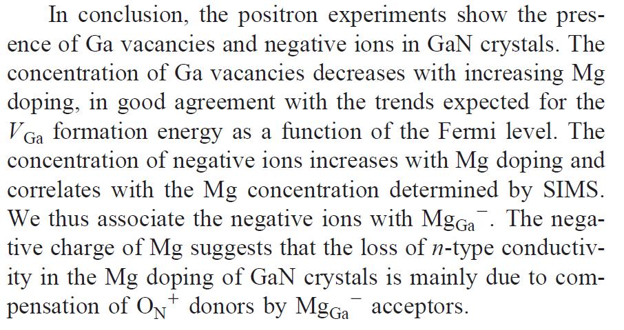
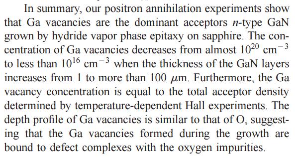
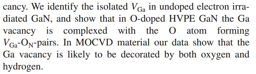
Positron Annihilation Spectroscopy on Defects in Semiconductors
|
|
|
- Elwin Logan
- 5 years ago
- Views:
Transcription

1 Positron Annihilation Spectroscopy on Defects in Semiconductors R. Krause-Rehberg Universität Halle, Inst. für Physik Some historical remarks Techniques of Positron Annihilation Study of Defects in Semiconductors User-dedicated Positron Facilities RK R

 Annihilation in matter was studied beginning in the 40 s Positrons can")
 first Identification of a positron in a cloud chamber 5 mm lead")
2 Discovery of the Positron Positron was predicted in 1928 by Paul A.M. Dirac Discovery in 1932 in cloud chamber pictures by C.D. Anderson P.A.M. Dirac C.D. Anderson Positronium as bound state of e - and e + lightest atom was predicted (1934) and discovered (1951) Annihilation in matter was studied beginning in the 40 s Positrons can be obtained by - pair production from gamma radiation (E > 1022 kev) - β + decay from isotopes (mostly 22 Na) first Identification of a positron in a cloud chamber 5 mm lead plate photo taken by C.D. Anderson
3 Electron structure of solids can be discovered during annihilation: conservation laws must be fulfilled (energy, momentum) positron cools down to thermal energies -> energy of annihilating electron-positron pair = energy of electron electron momentum distribution can directly be measured
4 2D ACAR (Angular Correlation of Annihilation Radiation) now: two-dimensional (position-sensitive) detectors measurement of single crystals in different directions: reconstruction of Fermi surface possible
5 2D-ACAR of Copper Theory Experiment p z along [100] Fermi surface of copper p y along [010] (Berko, 1979)
6 Positrons are sensitive for Crystal Lattice Defects : in addition to ACAR -> different experimental techniques were developed Positron lifetime spectroscopy and Doppler broadening spectroscopy end of 60s: lifetime is sensitive to lattice imperfections - Brandt et al. (1968): vacancies in ionic crystals - Dekhtyar et al. (1969): plastically deformed semiconductors - MacKenzie et al. (1967): vacancies in thermal equilibrium in metals Positrons are localized (trapped) by openvolume defects
7 Vacancies in thermal Equilibrium Vacancy concentration in thermal equilibrium: in metals H F ev at T m [1v] /atom fits well to the sensitivity range of positron annihilation Tungsten W parameter fit to trapping model (Ziegler, 1979) Temperature (K)
 and 0.")
8 22 Na The positron lifetime spectroscopy positron wave-function can be localized in the attractive potential of a defect annihilation parameters change in the localized state e.g. positron lifetime increases in a vacancy lifetime is measured as time difference between appearance of 1.27 (start) and 0.51 MeV (stop) quanta defect identification and quantification possible 18:42
9 Sensitivity limits of PAS for vacancy detection lower sensitivity limit e.g. for negatively charged divacancies in Si starts at about cm -3 upper limit: saturated positron trapping defect identification still possible Then: only lower limit for defect density can be given
10 Vacancies in a semiconductor may be charged in a metal: charge of a vacancy is effectively screened by free electrons they are not available in semiconductors thus, long-range Coulomb potential added positrons may be attracted or repelled trapping coefficient is function of charge state
11 Digital positron lifetime measurement

12 Screenshot of two digitized anode pulses time difference = samples = ps
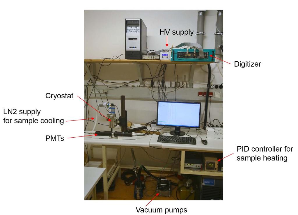
13
14 Positron lifetime spectroscopy Counts b = 218 ps (bulk) As grown Cz Si Plastically deformed Si 2 = 320 ps (divacancies) 3 = 520 ps (vacancy clusters) positron lifetime spectra consist of exponential decay components positron trapping in open-volume defects leads to long-lived components longer lifetime due to lower electron density analysis by non-linear fitting: lifetimes i and intensities I i positron lifetime spectrum: trapping coefficient Time [ns] trapping rate defect concentration
15 Doppler Broadening Spectroscopy
16 Measurement of Doppler Broadening electron momentum in propagation direction of 511 kev -ray leads to Doppler broadening of annihilation line can be detected by conventional energy-dispersive Ge detectors and standard electronics

17 Line Shape Parameters S parameter: S = A S /A 0 W parameter: W = A W /A 0 W parameter mainly determined by annihilations of core electrons (chemical information)

18 Doppler Coincidence Spectroscopy coincident detection of second annihilation reduces background use of a second Ge detector improves energy resolution of system

19 Doppler Coincidence Spectra E 1 +E 2 = 2 m 0 c 2 =1022 kev
20 Doppler-Coincidence-Spectroscopy in GaAs Chemical sensitivity due to electrons at high momentum (core electrons) a single impurity atom aside a vacancy is detectable examples: V Ga -Te As in GaAs:Te J. Gebauer et al., Phys. Rev. B 60 (1999) :42
21 Moderation of Positrons Mean implantation depth of un-moderated positrons from a 22-Na source (1/e) in Si: 50µm broad + positron emission spectrum deep implantation into solids not useful for study of defects in thin layers for defect depth profiling: moderation necessary monoenergetic positrons can be implanted to different depth

22 Moderation of Positrons moderation efficiency: 10-4
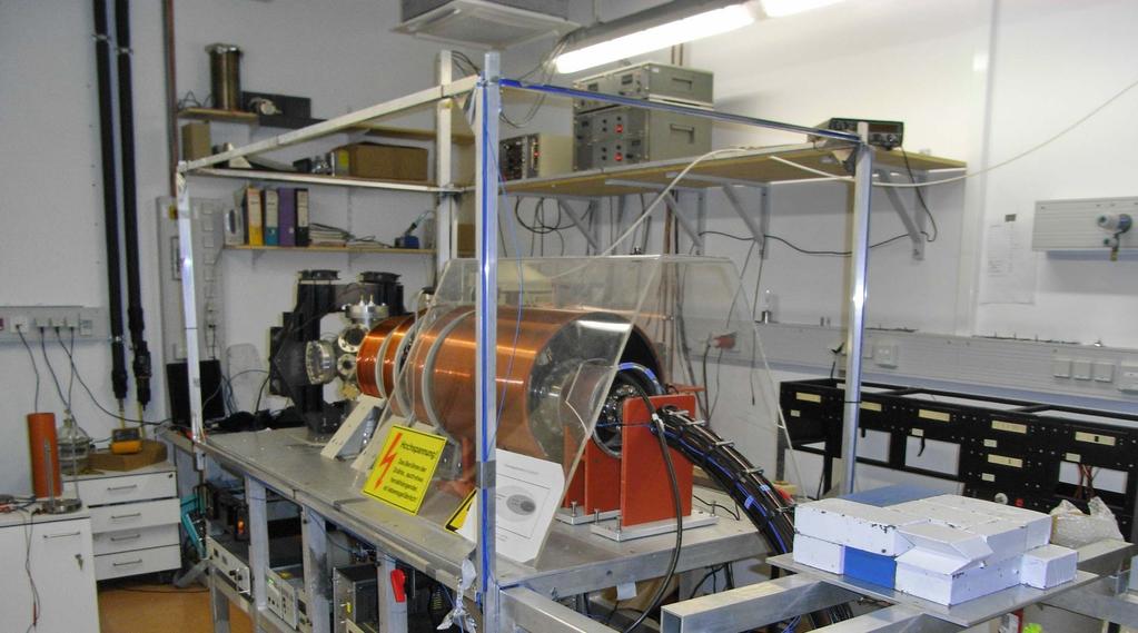
23 The Positron Beam System at Halle University spot diameter: 4 mm time per single Doppler measurement: 20 min time per depth scan: 8 hours no lifetime measurements
24
25 Defects in Si induced by Ion Implantation ion implantation is most important doping technique in planar technology main problem: generation of defects positron beam measurements (Eichler et al., 1997)

26 Point defects determine properties of materials Galliumphosphide 1 cm Point defects determine electronic and optical properties without vacancies transparent with 0.001% vacancies opaque 1 vacancy in atoms Point defects are generated by crystal growth, irradiation, by plastic deformation, by diffusion, Metals in high radiation environment -> formation of voids -> embrittlement
27 Defects in electron-irradiated Ge Electron irradiation (2 4K) induces Frenkel pairs (vacancy - interstitial pairs) steep annealing stage at 200 K at high irradiation dose: divacancies are formed (thermally more stable) Ge e - irr. at 4K (Polity et al., 1997)
 Equilibrium Phase Diagram of GaAs T sample : 1100 C Jurisch, Wenzl;")
28 GaAs: annealing under defined As-partial pressure two-zone-furnace: Control of sample temperature and As partial pressure allows T As : determines As-partial pressure navigate freely in phase diagram (existence area of compound) Equilibrium Phase Diagram of GaAs T sample : 1100 C Jurisch, Wenzl; 2002
29 GaAs: Annealing under defined As pressure Si Ga -V Ga Te As -V Ga GaAs:Si GaAs:Te Vacancy concentration (cm -3 ) Linear fit 0,01 0, Arsenic pressure (bar) Thermodynamic reaction: 1/4 As 4 gas As As + V Ga Vacancy concentration (cm -3 ) [Te] in cm -3 6x x x x , Arsenic pressure (bar) av at 550 K (ps) J. Gebauer et al., Physica B , 705 (1999) Mass action law: [V Ga ] = K VG p As 1/4 Fit: [V Ga -Dopant] ~ p As n n = 1/4
30 Comparison of doped and undoped GaAs Thermodynamic reaction: As As V As + 1/4As 4 gas Mass action law: [V As ] = K VAs p As -1/4 Fit: [V-complex] ~ p As n n = -1/4 undoped GaAs: As vacancy Bondarenko et al., 2003
31 EL2 in GaAs: important Antisite Defect interesting feature: EL2 exhibits metastability illumination at low temperature properties changes (e.g. no IR absorption any more) many structural models were discussed Dabrowski/Scheffler and Chadi/Chang: EL2 is isolated As Ga and in metastable state the antisite atom moves outward and leaves a V Ga Metastability is lost during warming-up to 115 K
32 EL2 in GaAs: important antisite Defect before annihilation, diffusing positrons can be trapped by such defects as a consequence: positron lifetime increases due to the reduced electron density in the vacancy experiment shows the existence of a Ga vacancy in the metastable state of GaAs, which does not exist in stable ground state was prove of As Ga model of EL2 R. Krause et al.: Observation of a monovacancy in the metastable state of the EL2 defect in GaAs by positron annihilation Phys. Rev. Lett. 65 (26), (1990).
33 DX Center in GaAlSb GaAlSb:Te defect appears in doped quasi-ternary III-V compound semiconductors (e.g. Al x Ga 1-x As, Al x Ga 1-x Sb) is complex: donor-? (so-called DX center) also shows metastable state at low temperatures model of Dabrowski/Scheffler predicted vacancy in stable state and the disappearance of this vacancy in metastable state also proved by positron annihilation Ga Sb Te Al Ga Sb Te Al Photoconductivity [S] Average positron lifetime [ps] Illumination Illumination metastable stable Annealing temperature [K] R. Krause-Rehberg et al., Phys. Rev. B 48 (1993) 11723
34 Compensating Defects in GaAs:Si Si is also often used as donor in GaAs Si is built-in as Si Ga+ and also as Si - As (amphoteric behavior) degree of compensation not constant, but growing with Si content result: doping only possible up to cm -3 at higher Si content: almost complete auto-compensation model for additional compensating center (acceptor): V Ga Si - Ga (K. Saarinen et. al, Helsinki UT)
![Identification of V Ga -Si Ga -Complexes in GaAs:Si Height [nm] 0.2 0.1 0.0 occupied empty states -2.0 V +1.](/docs-images/95/125867092/images/35-0.jpg "4 V 123456789 123456789 lattice spacing in [110] direction Scanning tunneling microscopy at GaAs (110)- cleavages planes (by Ph.")
 Quantification Agreement Mono-vacancies in GaAs:Si are V Ga -Si Ga -complexes Gebauer et")
35 Identification of V Ga -Si Ga -Complexes in GaAs:Si Height [nm] occupied empty states -2.0 V +1.4 V lattice spacing in [110] direction Scanning tunneling microscopy at GaAs (110)- cleavages planes (by Ph. Ebert, Jülich) Defect complex identified as V Ga -Si Ga Defect concentration (cm -3 ) Positrons - c vac STM - [Si Ga -V Ga ] Si concentration (cm -3 ) Quantification Agreement Mono-vacancies in GaAs:Si are V Ga -Si Ga -complexes Gebauer et al., Phys. Rev. Lett. 78 (1997) 3334
36 Vacancy clusters in semiconductors vacancy clusters were observed after neutron irradiation, ion implantation and plastic deformation due to large open volume (low electron density) -> positron lifetime increases distinctly example: plastically deformed Ge lifetime: = 525 ps reason for void formation: jog dragging mechanism trapping rate of voids disappears during annealing experiment Krause-Rehberg et al., 1993
37 Theoretical calculation of vacancy clusters in Si there are cluster configurations with a large energy gain Magic Numbers with 6, 10 und 14 vacancies positron lifetime increases distinctly with cluster size for n > 10 saturation effect, i.e. size cannot be determined T.E.M. Staab et al., Physica B (1999)
38 as-grown GaN (FCM GmbH) Defect studies of GaN 950 C 1050 C 980 C

39 [Ga vacancies] cm -3
40
41
42
43
44
45
46
47
48
49
50
51 o-positronium Lifetime allows Porosimetry In materials without free electrons Positronium may be formed (Polymers, glass, liquids, gases) p-ps annihilates without interaction with host material o-ps lifetime in vacuum 142 ns in matter: positron may pick off another electron with opposite spin -> fast annihilation with two gammas 25% 75%

52 Pick-off Annihilation positrons form Ps pick-off annihilation: o-ps is converted to p-ps by capturing an electron with anti-parallel spin happens during collisions at walls of pore lifetime decreases rapidly lifetime is function of pore size 1.5 ns to 142 ns = 125 ps = ns

53 o-ps lifetime 4 versus pore size in CPG Glass we measured porous CPG glass in a broad pore size range RTE model given pore size obtained by N 2 -adsorption and/or mercury intrusion technique for T=300 K fair agreement to the RTE model S.Thränert, Dissertation, MLU Halle 2008
54 User-dedicated intense Positron Sources in Germany Two intense positron sources available (positrons by pair production) NEPOMUC (NEutron induced POsitron Source MUniCh) at FRM-II PLEPS (monoenergetic positron lifetime system) PAES (Positron-induced Auger Electron Spectroscopy) CDBS (Coincidence Doppler Broadening Spectroscopy) SCM (Scanning Positron Microscope) user beam line EPOS (ELBE Positron Source) at Helmholtz Center Dresden-Rossendorf MePS (Mono-energetic Positron Spectroscopy) GiPS (Gamma-induced Positron Spectroscopy) CoPS (conventional setup using 22Na sources) at both sites: web-based application system for beam time 18:42
55 NEPOMUC at FRM II SR 11 Remoderator PLEPS Switch SPM interface PAES CDBS Open Beamport: Ps -
56 Munich Positron Scanning Microscope Lateral Resolution with Scanning Positron Microscope lateral resolution 1 2 µm Positron lifetime spectroscopy lateral resolution principally limited by positron diffusion (L + 100nm) W. Triftshäuser et al., NIM B 130 (1997) 265

57 Microhardness indentation in GaAs Comparison of SEM and Munich Positron Scanning Microscope SEM problem here at the moment: intensity in future: adaption to NEPOMUC at FRM-II Positrons Krause-Rehberg et al., 2002 Halle
58 Defects in high-energy self-implanted Si: The Rp/2 effect after high-energy (3.5 MeV) self-implantation of Si (5x10 15 cm -2 ) and RTA annealing (900 C, 30s): two new gettering zones appear at Rp and Rp/2 (Rp = projected range of Si + ) visible by SIMS profiling after intentional Cu contamination TEM image by P. Werner, MPI Halle Cu concentration (cm -3 ) R p / Depth ( m) R p SIMS at R p : gettering by interstitial-type dislocation loops (formed by excess interstitials during RTA) no defects visible by TEM at Rp/2 What type are these defects? 18:42
59 Investigation of the Rp/2 effect by conventional VEPAS Positron energy (kev) the defect layers are expected in a depth of 1.7 mm and 2.8 mm corresponding to E + = 18 and 25 kev implantation profile too broad to discriminate between the two zones simulation of S(E) curve gives the same result for assumed blue and yellow defect profile (solid line in upper panel) furthermore: small effect only no conclusions about origin of R p /2 effect possible bulk S/S defect density (cm -3 ) P(z,E) kev R p /2 R p 18 kev reference implanted and annealed + Cu 25 kev Depth ( m)
60 Enhanced depth resolution by using the Positron Microscope defect depth 10 m positron microbeam E = 8 kev scan direction lateral resolution m sample is wedge-shaped polished (0.5 2 ) layer of polishing defects must be thin compared to e + implantation depth best: chemo-mechanical polishing positron lifetime (ps) defect bulk 0 1 mm scan width
 beam energy of 8 kev: mean penetration depth is about 400 nm; represents optimum depth resolution no further improvement possible due to positron diffusion: L + (Si @ 300K)» 230 nm both regions")
61 First defect depth profile using Positron Microscopy 45 lifetime spectra: scan along wedge separation of 11 µm between two measurements corresponds to depth difference of 155 nm (α = 0.81 ) beam energy of 8 kev: mean penetration depth is about 400 nm; represents optimum depth resolution no further improvement possible due to positron diffusion: L + 300K)» 230 nm both regions well visible: vacancy clusters with increasing density down to 2 µm (R p /2 region) in R p region: lifetime 2 = 330 ps; corresponds to open volume of a divacancy; must be stabilized or being part of interstitial-type dislocation loops excellent agreement with gettered Cu profile 2 (ps) average lifetime (ps) 0,8 0,6 0, R. Krause-Rehberg et al., Appl. Phys. Lett. 77 (2000) microvoids surface R p /2 R p fraction of trapped positrons defect-related lifetime divacancy-type defect Silicon self-implantation MeV, cm -2 - annealed 30s 900 C - Cu contaminated bulk silicon depth (µm) Cu SIMS-Profil
62 EPOS = ELBE Positron Source ELBE -> electron LINAC (40 MeV and up to 40 kw) in HZDR Research Center Dresden-Rossendorf EPOS -> collaboration of Univ. Halle with HZDR EPOS will be the combination of a positron lifetime spectrometer, Doppler coincidence, and AMOC User-dedicated facility main features: - high-intensity bunched positron beam (E + = kev) - very good time resolution by using the unique primary time structure of ELBE - digital multi-detector array - fully remote control via internet by user 18:42

63 Ground plan of the ELBE hall

64 MePS scheme

65 Cave 111b electron-positron converter electron beam line

66
67 Beam time in September 2011 First successful application: low-k Layers low-k dielectric layers shall replace SiO 2 as isolation in CPU s higher speed possible because =RC decreases high-quality spectra already without chopper 18:42
, no activation of samples by -n processes was found average electron current 1 ma = 20 kw beam power; electron beam dump outside lab thus gamma")
68 Bremsstrahlung Gamma Source of ELBE (FZ Dresden-Rossendorf) Pulsed gamma source using superconductive Linac ELBE repetition frequency 26 MHz (or smaller by factor 2 n ) in CW mode! bunch length < 5 ps up to 20 MeV (we used 16 MeV), no activation of samples by -n processes was found average electron current 1 ma = 20 kw beam power; electron beam dump outside lab thus gamma background at target position is very low (Ge detectors with 100% efficiency) Ideal for GiPS! Is now part of EPOS project user dedicated positron source.
69 GiPS: Gamma-induced Positron Spectroscopy AMOC: Age Momentum Correlation CDBS : Concidence Doppler Broadening Spectroscopy 3 coincident setups were used: 2 AMOC and 1 CDBS spectrometer only coincident detection ensures high spectra quality

70 The GiPS setup includes 8 Detectors (4 Ge and 4 BaF 2 )
71 total count rate in spectrum: 12x10 6 Example: Water at RT conventional spectrum GiPS measurement Black spectrum: conventional measurement by Kotera et al., Phys. Lett. A 345, (2005) 184
72 Conclusions Positrons are a unique tool for characterization of vacancy-type defects in crystalline solids for embedded nano-particles (e.g. small precipitates) for porosimetry ( nm) New facilities become available for user-dedicated operation having better time resolution and spectra quality much higher intensity FRM-II: lateral resolution 1 µm This presentation can be found as pdf-file on our Website: reinhard.krause-rehberg@physik.uni-halle.de
73 Thank you for your attention! 18:42
Material Science using Positron Annihilation
 Material Science using Positron Annihilation R. Krause-Rehberg Universität Halle, Inst. für Physik 9.3.2018 Some historical remarks Techniques of Positron Annihilation Study of Defects in Semiconductors
Positron Annihilation in Materials Science
 Positron Annihilation in Materials Science R. Krause-Rehberg Universität Halle, Inst. für Physik History Techniques of Positron Annihilation Defects in Semiconductors User-dedicated Positron Facilities
in Si by means of Positron Annihilation
 Investigation of the Rp/2 /2-effect in Si by means of Positron Annihilation R. Krause-Rehberg, F. Börner, F. Redmann Universität Halle Martin-Luther-Universität R. Kögler, W. Skorupa Forschungszentrum
Outlook: Application of Positron Annihilation for defects investigations in thin films. Introduction to Positron Annihilation Methods
 Application of Positron Annihilation for defects investigations in thin films V. Bondarenko, R. Krause-Rehberg Martin-Luther-University Halle-Wittenberg, Halle, Germany Outlook: Introduction to Positron
Identification of Getter Defects in high-energy self-implanted Silicon at Rp/2
 Identification of Getter Defects in high-energy self-implanted Silicon at Rp R. Krause-Rehberg 1, F. Börner 1, F. Redmann 1, J. Gebauer 1, R. Kögler 2, R. Kliemann 2, W. Skorupa 2, W. Egger 3, G. Kögel
Research Center Dresden Rossendorf
 News of the EPOS Project at the ELBE Radiation Source in the Research Center Dresden Rossendorf EPOS-Team & R. Krause-Rehberg Extended Concept of EPOS Progress of the mono-energetic Positron Beam (MePS)
Introduction into Positron Annihilation
 Introduction into Positron Annihilation Introduction (How to get positrons? What is special about positron annihilation?) The methods of positron annihilation (positron lifetime, Doppler broadening, ACAR...)
2. Point Defects. R. Krause-Rehberg
 R. Krause-Rehberg 2. Point Defects (F-center in NaCl) 2.1 Introduction 2.2 Classification 2.3 Notation 2.4 Examples 2.5 Peculiarities in Semiconductors 2.6 Determination of Structure and Concentration
The intense, pulsed positron source EPOS at the Research Centre Dresden-Rossendorf
 The intense, pulsed positron source EPOS at the Research Centre Dresden-Rossendorf The EPOS Team and R. Krause-Rehberg Martin-Luther University, Halle-Wittenberg, Dept. of Physics, 06099 Halle / Germany
New Concept of EPOS Progress of the Mono-energetic Positron Beam (MePS) Gamma-induced Positron Spectroscopy (GiPS)
 Gamma-induced Positron Spectroscopy (GiPS)") Progress of the EPOS Project: Gamma Induced Positron Spectroscopy (GiPS) R. Krause-Rehberg 1,*,W.Anwand 2,G.Brauer 2, M. Butterling 1,T.Cowan 2,M. Jungmann 1, A. Krille 1, R. Schwengner 2, A. Wagner 2
Progress of the EPOS Project: Gamma Induced Positron Spectroscopy (GiPS) R. Krause-Rehberg 1,*,W.Anwand 2,G.Brauer 2, M. Butterling 1,T.Cowan 2,M. Jungmann 1, A. Krille 1, R. Schwengner 2, A. Wagner 2
Study of semiconductors with positrons. Outlook:
 Study of semiconductors with positrons V. Bondarenko, R. Krause-Rehberg Martin-Luther-University Halle-Wittenberg, Halle, Germany Introduction Positron trapping into defects Methods of positron annihilation
The EPOS System (ELBE Positron Source) at Helmholtz Centre Dresden- Rossendorf and first experiments at photovoltaic CIGS layers
 at Helmholtz Centre Dresden- Rossendorf and first experiments at photovoltaic CIGS layers") The EPOS System (ELBE Positron Source) at Helmholtz Centre Dresden- Rossendorf and first experiments at photovoltaic CIGS layers R. Krause-Rehberg 1, A. Wagner 2 and many colleagues of Univ. Halle and
The EPOS System (ELBE Positron Source) at Helmholtz Centre Dresden- Rossendorf and first experiments at photovoltaic CIGS layers R. Krause-Rehberg 1, A. Wagner 2 and many colleagues of Univ. Halle and
R. Krause-Rehberg. Martin-Luther-Universität Halle-Wittenberg. Positron Lifetime / Doppler Broadening / Angular Correlation / AMOC
 Experimental Techniques of Positron Annihilation and the pulsed Positron Source EPOS R. Krause-Rehberg -Wittenberg Techniques of Positron Annihilation Positron Sources Positron Lifetime / Doppler Broadening
The MePS System at Helmholtz-Zentrum Dresden-Rossendorf and its special Capability for Positronium Lifetime Spectroscopy
 The MePS System at Helmholtz-Zentrum Dresden-Rossendorf and its special Capability for Positronium Lifetime Spectroscopy R. Krause-Rehberg and many colleagues of Univ. Halle and HZDR Martin-Luther University
Basics and Means of Positron Annihilation
 Basics and Means of Positron Annihilation Positron history Means of positron annihilation positron lifetime spectroscopy angular correlation Doppler-broadening spectroscopy Near-surface positron experiments:
Positron Annihilation Spectroscopy - A non-destructive method for material testing -
 Maik Butterling Institute of Radiation Physics http://www.hzdr.de Positron Annihilation Spectroscopy - A non-destructive method for material testing - Maik Butterling Positron Annihilation Spectroscopy
EPOS an intense positron beam project at the Research Center Rossendorf
 EPOS an intense positron beam project at the Research Center Rossendorf R. Krause-Rehberg 1, G. Brauer 2, S. Sachert 1, V. Bondarenko 1, A. Rogov 2, K. Noack 2 1 Martin-Luther-University Halle 2 Research
The intense positron source EPOS at Research Center Rossendorf
 The intense positron source EPOS at Research Center Rossendorf R. Krause-Rehberg 1, G. Brauer 2, S. Sachert 1, A. Krille 1, V. Bondarenko 1 1 -Wittenberg 2 FZ Rossendorf Martin-Luther-Universität RK Halle
positron source EPOS - general concept - timing system - digital lifetime measurement
 The pulsed high-brightness positron source EPOS R. Krause-Rehberg 1, G. Brauer 2, A. Krille 1, M. Jungmann 1, S. Sachert 1, A. Rogov 2, K. Nowak 2 1 Martin-Luther-University Halle, Germany 2 Research Center
The intense Positron Source EPOS at ELBE Radiation Source of Research Center Rossendorf
 The intense Positron Source EPOS at ELBE Radiation Source of Research Center Rossendorf R. Krause-Rehberg 1, G. Brauer 2, 1 Martin-Luther-University Halle 2 Research Center Rossendorf Martin-Luther-Universität
Improvement of depth resolution of VEPAS by a sputtering technique
 Martin Luther University Halle Improvement of depth resolution of VEPAS by a sputtering technique R. Krause Rehberg, M. John, R. Böttger, W. Anwand and A. Wagner Martin Luther University Halle & HZDR Dresden
POSITRON AND POSITRONIUM INTERACTIONS WITH CONDENSED MATTER. Paul Coleman University of Bath
 POSITRON AND POSITRONIUM INTERACTIONS WITH CONDENSED MATTER Paul Coleman University of Bath THE FATE OF POSITRONS IN CONDENSED MATTER POSITRON-SURFACE INTERACTIONS positron backscattering BACKSCATTERED
Vacancy generation during Cu diffusion in GaAs M. Elsayed PhD. Student
 Vacancy generation during Cu diffusion in GaAs M. Elsayed PhD. Student Martin Luther University-FB Physik IV Halle-Wittenberg Outlines Principles of PAS vacancy in Semiconductors and shallow positron traps
Application of positrons in materials research
 Application of positrons in materials research Trapping of positrons at vacancy defects Using positrons, one can get defect information. R. Krause-Rehberg and H. S. Leipner, Positron annihilation in Semiconductors,
? Physics with many Positrons
 Varenna Summer School July 2009? Physics with many Positrons Positron Sources & Positron Beams Christoph Hugenschmidt Technische Universität München What is many? Galaxy: 1.5 10 43 e + /s! = 1 lake + 1
Positron Annihilation in Material Research
 Positron Annihilation in Material Research Introduction Positron sources, positron beams Interaction of positrons with matter Annihilation channels: Emission of 1, 2 or 3 γ-quanta Annihilation spectroscopies:
Vacancy-like defects in SI GaAs: post-growth treatment
 Vacancy-like defects in SI : post-growth treatment V. Bondarenko, R. Krause-Rehberg Martin-Luther-University Halle-Wittenberg, Halle, Germany B. Gruendig-Wendrock, J.R. Niklas TU Bergakademie Freiberg,
DEVELOPMENT OF A NEW POSITRON LIFETIME SPECTROSCOPY TECHNIQUE FOR DEFECT CHARACTERIZATION IN THICK MATERIALS
 Copyright JCPDS - International Centre for Diffraction Data 2004, Advances in X-ray Analysis, Volume 47. 59 DEVELOPMENT OF A NEW POSITRON LIFETIME SPECTROSCOPY TECHNIQUE FOR DEFECT CHARACTERIZATION IN
2. Point Defects. R. Krause-Rehberg
 R. Krause-Rehberg 2. Point Defects (F-center in acl) 2.1 Introduction 2.2 Classification 2.3 otation 2.4 Examples 2.5 Peculiarities in Semiconductors 2.6 Determination of Structure and Concentration 2.7
Department of Physics, Techno India Batanagar (Techno India Group), Kolkata , West Bengal, India.
, Kolkata , West Bengal, India.") Department of Physics, Techno India Batanagar (Techno India Group), Kolkata 700141, West Bengal, India. Visiting Scientists @ SINP, @VECC, @ IIEST Kolkata, India. nn.mondal2011@gmail.com, nagendra.n.mondal@biemsindia.org
Department of Physics, Techno India Batanagar (Techno India Group), Kolkata 700141, West Bengal, India. Visiting Scientists @ SINP, @VECC, @ IIEST Kolkata, India. nn.mondal2011@gmail.com, nagendra.n.mondal@biemsindia.org
Positron Annihilation techniques for material defect studies
 Positron Annihilation techniques for material defect studies H. Schut Section : Neutron and Positron Methods in Materials (NPM 2 ) Department: Radiation, Radionuclides and Reactors (R 3 ) Faculty of Applied
Positron Annihilation Spectroscopy
 Positron Annihilation Spectroscopy (1) Angular Correlation θ N x, y = p x, y m C θ γ-ray (511keV ± E) 0 (2) Doppler Broadening Cp E = z 2 θ N p ~100µm 22 Na (e + Source) e - e + ~ 10-12 s Sample γ-ray
M. Werner, E. Altstadt, M. Jungmann, G. Brauer, K. Noack, A. Rogov, R. Krause-Rehberg. Thermal Analysis of EPOS components
 M. Werner, E. Altstadt, M. Jungmann, G. Brauer, K. Noack, A. Rogov, R. Krause-Rehberg Thermal Analysis of EPOS components Dresden, June 27, 2008 Page 2 FZD Abstract: We present a simulation study of the
Slow-Positron-Beam Techniques
 Slow-Positron-Beam Techniques 1 Slow-Positron-Beam Techniques The main advantage of the conventional sample source sandwich arrangement is that the emitted positrons immediately penetrate the sample. A
Development status of the positron lifetime beam MePS and the first lifetime measurements of porous ultra-low-k dielectrics with MePS
 Development status of the positron lifetime beam MePS and the first lifetime measurements of porous ultra-low-k dielectrics with MePS Institut für Physik, Martin-Luther-Universität Halle-Wittenberg Table
Characterisation of mesopores - ortho-positronium lifetime measurement as a porosimetry technique
 Characterisation of mesopores - ortho-positronium lifetime measurement as a porosimetry technique S. Thraenert 1, E. M. Hassan 1, D. Enke 2, R. Krause-Rehberg 1 Martin-Luther-Universität Halle-Wittenberg
Investigation of SiC by Positrons
 nd/march/000/erlangen Investigation of SiC by Positrons Atsuo KAWASUSO Martin-Luther-Universität Halle-Wittenberg (Humboldt Research Fellow) Japan Atomic Energy Research Institute Takasaki Establishment
Defect chemistry in GaAs studied by two-zone annealings under defined As vapor pressure. Outlook:
 Defect chemistry in studied by two-zone annealings under defined vapor pressure V. Bondarenko 1, R. Krause-Rehberg 1, J. Gebauer 2, F. Redmann 1 1 Martin-Luther-University Halle-Wittenberg, Halle, Germany
Positron theoretical prediction
 Positron theoretical prediction Schrödinger equation: ˆ 2 p x, t Vx, t x, t i 22 m tt non-relativistic equation of motion for electron Erwin Schrödinger 1933 Nobel prize Positron theoretical prediction
Positron Annihilation Lifetime Spectroscopy (PALS)
") Positron Annihilation Lifetime Spectroscopy (PALS) Javier Puertas 12/12/12 Contents 1. Introduction. 1.1. General idea of the process. 3. PALS: Experimental results. 1.2. What is a positron? 3.1. Math.
Positron Annihilation Lifetime Spectroscopy (PALS) Javier Puertas 12/12/12 Contents 1. Introduction. 1.1. General idea of the process. 3. PALS: Experimental results. 1.2. What is a positron? 3.1. Math.
Positron Annihilation as tool in materials science. R. Krause-Rehberg, Dept. of Physics, University Halle
 Positron Annihilation as tool in materials science R. Krause-Rehberg, Dept. of Physics, University Halle Content 40 Years of positron research in Halle Methods of positron annihilation Positron Lifetime
Minimal Update of Solid State Physics
 Minimal Update of Solid State Physics It is expected that participants are acquainted with basics of solid state physics. Therefore here we will refresh only those aspects, which are absolutely necessary
PRINCIPLES OF POSITRON ANNIHILATION
 1.1. Introduction The phenomenon of positron annihilation spectroscopy (PAS) has been utilized as nuclear method to probe a variety of material properties as well as to research problems in solid state
Positron Probe Microanalyzer (PPMA) facilities at AIST
 facilities at AIST") Positron Probe Microanalyzer (PPMA) and other accelerator based slow positron facilities at AIST B. E. O Rourke, N. Oshima, A. Kinomura, T. Ohdaira and R. Suzuki National Institute of Advanced Industrial
Positron Probe Microanalyzer (PPMA) and other accelerator based slow positron facilities at AIST B. E. O Rourke, N. Oshima, A. Kinomura, T. Ohdaira and R. Suzuki National Institute of Advanced Industrial
Motivation. g-spectroscopy deals with g-ray detection and is one of the most relevant methods to investigate excited states in nuclei.
 Motivation Spins and excited states of double-magic nucleus 16 O Decay spectra are caused by electro-magnetic transitions. g-spectroscopy deals with g-ray detection and is one of the most relevant methods
Joint ICTP-IAEA Workshop on Physics of Radiation Effect and its Simulation for Non-Metallic Condensed Matter.
 2359-3 Joint ICTP-IAEA Workshop on Physics of Radiation Effect and its Simulation for Non-Metallic Condensed Matter 13-24 August 2012 Electrically active defects in semiconductors induced by radiation
The appearance of vacancies during Cu and Zn diffusion in III-V compound semiconductors
 The appearance of vacancies during Cu and Zn diffusion in III-V compound semiconductors Dissertation zur Erlangung des akademischen Grades Dr. rerum naturalium (Dr. rer. nat.) vorgelegt der Mathematisch-Naturwissenschaftlich-Technischen
Identification of the 0.95 ev luminescence band in n-type GaAs:Si
 INSTITUTE OF PHYSICS PUBLISHING JOURNAL OF PHYSICS: CONDENSED MATTER J. Phys.: Condens. Matter 15 (2003) 1 7 PII: S0953-8984(03)66937-7 Identification of the 0.95 ev luminescence band in n-type GaAs:Si
Photoionization of the silicon divacancy studied by positron-annihilation spectroscopy
 PHYSICAL REVIEW B VOLUME 57, NUMBER 20 15 MAY 1998-II Photoionization of the silicon divacancy studied by positron-annihilation spectroscopy H. Kauppinen* and C. Corbel Institut National des Sciences et
Unmanageable Defects in Proton- Irradiated Silicon: a Factual Outlook for Positron Probing N. Yu. Arutyunov 1,2, M. Elsayed 1, R.
 Unmanageable Defects in Proton- Irradiated Silicon: a Factual Outlook for Positron Probing N. Yu. Arutyunov 1,2, M. Elsayed 1, R. Krause-Rehberg 1 1 Department of Physics, Martin Luther University, 06120
EE 212 FALL ION IMPLANTATION - Chapter 8 Basic Concepts
 EE 212 FALL 1999-00 ION IMPLANTATION - Chapter 8 Basic Concepts Ion implantation is the dominant method of doping used today. In spite of creating enormous lattice damage it is favored because: Large range
DETECTORS. I. Charged Particle Detectors
 DETECTORS I. Charged Particle Detectors A. Scintillators B. Gas Detectors 1. Ionization Chambers 2. Proportional Counters 3. Avalanche detectors 4. Geiger-Muller counters 5. Spark detectors C. Solid State
Ion Implantation ECE723
 Ion Implantation Topic covered: Process and Advantages of Ion Implantation Ion Distribution and Removal of Lattice Damage Simulation of Ion Implantation Range of Implanted Ions Ion Implantation is the
STRESS ANALYSIS USING BREMSSTRAHLUNG RADIATION
 Copyright JCPDS - International Centre for Diffraction Data 2003, Advances in X-ray Analysis, Volume 46. 106 STRESS ANALYSIS USING BREMSSTRAHLUNG RADIATION F. A. Selim 1, D.P. Wells 1, J. F. Harmon 1,
Review of Optical Properties of Materials
 Review of Optical Properties of Materials Review of optics Absorption in semiconductors: qualitative discussion Derivation of Optical Absorption Coefficient in Direct Semiconductors Photons When dealing
ION IMPLANTATION - Chapter 8 Basic Concepts
 ION IMPLANTATION - Chapter 8 Basic Concepts Ion implantation is the dominant method of doping used today. In spite of creating enormous lattice damage it is favored because: Large range of doses - 1 11
CHAPTER-II Experimental Techniques and Data Analysis (Positron annihilation spectroscopy)
") CHAPTER-II Experimental Techniques and Data Analysis (Positron annihilation spectroscopy) 64 Techniques in Positron annihilation spectroscopy PAS comprises of different techniques which provide information
CHAPTER-II Experimental Techniques and Data Analysis (Positron annihilation spectroscopy) 64 Techniques in Positron annihilation spectroscopy PAS comprises of different techniques which provide information
SURVEY OF RECENT RADIATION DAMGE STUDIES AT HAMBURG
 SURVEY OF RECENT RADIATION DAMGE STUDIES AT HAMBURG E. Fretwurst 1, D. Contarato 1, F. Hönniger 1, G. Kramberger 2 G. Lindström 1, I. Pintilie 1,3, A. Schramm 1, J. Stahl 1 1 Institute for Experimental
SLOW-POSITRON IMPLANTATION SPECTROSCOPY IN NANOSCIENCE *
 SLOW-POSITRON IMPLANTATION SPECTROSCOPY IN NANOSCIENCE * Ivan PROCHÁZKA a, Jakub ČÍŽEK a, Gerhard BRAUER b, Wolfgang ANWAND b a Department of Low Temperature Physics, Faculty of Mathematics and Physics,
David B. Cassidy. Department of Physics and Astronomy, University of California, Riverside, USA. Varenna, July 09
 Experimental production of many- positron systems: L2, techniques David B. Cassidy Department of Physics and Astronomy, University of California, Riverside, USA cassidy@physics.ucr.edu Varenna, July 09
EEE4106Z Radiation Interactions & Detection
 EEE4106Z Radiation Interactions & Detection 2. Radiation Detection Dr. Steve Peterson 5.14 RW James Department of Physics University of Cape Town steve.peterson@uct.ac.za May 06, 2015 EEE4106Z :: Radiation
characterization in solids
 Electrical methods for the defect characterization in solids 1. Electrical residual resistivity in metals 2. Hall effect in semiconductors 3. Deep Level Transient Spectroscopy - DLTS Electrical conductivity
Semiconductor X-Ray Detectors. Tobias Eggert Ketek GmbH
 Semiconductor X-Ray Detectors Tobias Eggert Ketek GmbH Semiconductor X-Ray Detectors Part A Principles of Semiconductor Detectors 1. Basic Principles 2. Typical Applications 3. Planar Technology 4. Read-out
Session 5: Solid State Physics. Charge Mobility Drift Diffusion Recombination-Generation
 Session 5: Solid State Physics Charge Mobility Drift Diffusion Recombination-Generation 1 Outline A B C D E F G H I J 2 Mobile Charge Carriers in Semiconductors Three primary types of carrier action occur
Study on Bose-Einstein Condensation of Positronium
 Study on Bose-Einstein Condensation of Positronium K. Shu 1, T. Murayoshi 1, X. Fan 1, A. Ishida 1, T. Yamazaki 1,T. Namba 1,S. Asai 1, K. Yoshioka 2, M. Kuwata-Gonokami 1, N. Oshima 3, B. E. O Rourke
Defect structure and oxygen diffusion in PZT ceramics
 Defect structure and oxygen diffusion in PZT ceramics Adam Georg Balogh Institute of Materials Science Technische Universität Darmstadt A. G. Balogh Folie 1 Introduction Ferroelectrics are of great technical
Advantages / Disadvantages of semiconductor detectors
 Advantages / Disadvantages of semiconductor detectors Semiconductor detectors have a high density (compared to gas detector) large energy loss in a short distance diffusion effect is smaller than in gas
National Institute of Materials Physics Bucharest-Magurele. Cristian-Mihail Teodorescu, PhD, S.R.1, Surfaces and Interfaces,
 National Institute of Materials Physics Bucharest-Magurele ELI-NP Cristian-Mihail Teodorescu, PhD, S.R.1, Surfaces and Interfaces, teodorescu@infim.ro National Institute of Materials Physics Bucharest-Magurele
Positron Lifetime Spectroscopy of Silicon Nanocontainers for Cancer Theranostic Applications
 The 2nd International Symposium on Physics, Engineering and Technologies for Biomedicine Volume 2018 Conference Paper Positron Lifetime Spectroscopy of Silicon Nanocontainers for Cancer Theranostic Applications
ASPECTS OF THE MCMASTER INTENSE POSITRON BEAM FACILITY
 ASPECTS OF THE MCMASTER INTENSE POSITRON BEAM FACILITY ASPECTS OF THE MCMASTER INTENSE POSITRON BEAM FACILITY (MIPBF) By PEIHAI LI M.Eng., B.Sc. A Thesis Submitted to the School of Graduate Studies in
ATHENA / AD-1. First production and detection of cold antihydrogen atoms. ATHENA Collaboration. Rolf Landua CERN
 ATHENA / AD-1 First production and detection of cold antihydrogen atoms ATHENA Collaboration Rolf Landua CERN 1 LONG TERM PHYSICS GOALS Antihydrogen = Hydrogen? CPT Gravity But... 2 FIRST GOAL PRODUCTION
A semiconductor is an almost insulating material, in which by contamination (doping) positive or negative charge carriers can be introduced.
 positive or negative charge carriers can be introduced.") Semiconductor A semiconductor is an almost insulating material, in which by contamination (doping) positive or negative charge carriers can be introduced. Page 2 Semiconductor materials Page 3 Energy levels
Semiconductor A semiconductor is an almost insulating material, in which by contamination (doping) positive or negative charge carriers can be introduced. Page 2 Semiconductor materials Page 3 Energy levels
08 - Miscellaneous and historical detectors
 08 - Miscellaneous and historical detectors Jaroslav Adam Czech Technical University in Prague Version 2 Jaroslav Adam (CTU, Prague) DPD_08, Miscellaneous and historical detectors Version 2 1 / 25 Streamer
Positron Beam Lifetime Spectroscopy at
 UCRL-JC-124616 PREPRINT Positron Beam Lifetime Spectroscopy at Lawrence Livermore National Laboratory R. Howell T. Cowan J. Hartley P. Stern This paper was prepared for submittal to the 14th International
Testing and Evaluation of Scintillators
 Institut für Physik, Martin-Luther-Universität Halle-Wittenberg February 18th, 2009 Preface: Moved to IZM (With a Little Help from my Friends) Preface: Proud Father Preface: Table of Contents 1 Preface
Interaction of ion beams with matter
 Interaction of ion beams with matter Introduction Nuclear and electronic energy loss Radiation damage process Displacements by nuclear stopping Defects by electronic energy loss Defect-free irradiation
The annealing of interstitial carbon atoms in high resistivity n-type silicon after proton irradiation
 ROSE/TN/2002-01 The annealing of interstitial carbon atoms in high resistivity n-type silicon after proton irradiation M. Kuhnke a,, E. Fretwurst b, G. Lindstroem b a Department of Electronic and Computer
Hussein Ayedh. PhD Studet Department of Physics
 Hussein Ayedh PhD Studet Department of Physics OUTLINE Introduction Semiconductors Basics DLTS Theory DLTS Requirements Example Summary Introduction Energetically "deep trapping levels in semiconductor
Laboratory of Nuclear Solid State Physics, USTC
 IV Laboratory of Nuclear Solid State Physics, USTC 5. e+e e+e- 2 180 180 e+e e+e- 2 CDB CDB, 2D 2D-ACAR ACAR e+ e+-e- CDB CDB 2D 2D-ACAR 1 = x y ρ 2γ z N ( p, p ) ( p) dp γ D ( p ) ρ ( p) dp z = 2 y dp
Positron-Annihilation Lifetime Spectroscopy at a Superconducting Electron Accelerator
 Positron-Annihilation Lifetime Spectroscopy at a Superconducting Electron Accelerator Andreas Wagner Nuclear Physics Division Institute of Radiation Physics The team Helmholtz-Zentrum Dresden-Rossendorf
Semiconductor-Detectors
 Semiconductor-Detectors 1 Motivation ~ 195: Discovery that pn-- junctions can be used to detect particles. Semiconductor detectors used for energy measurements ( Germanium) Since ~ 3 years: Semiconductor
Single ion implantation for nanoelectronics and the application to biological systems. Iwao Ohdomari Waseda University Tokyo, Japan
 Single ion implantation for nanoelectronics and the application to biological systems Iwao Ohdomari Waseda University Tokyo, Japan Contents 1.History of single ion implantation (SII) 2.Novel applications
Energetic particles and their detection in situ (particle detectors) Part II. George Gloeckler
 Part II. George Gloeckler") Energetic particles and their detection in situ (particle detectors) Part II George Gloeckler University of Michigan, Ann Arbor, MI University of Maryland, College Park, MD Simple particle detectors Gas-filled
Energetic particles and their detection in situ (particle detectors) Part II George Gloeckler University of Michigan, Ann Arbor, MI University of Maryland, College Park, MD Simple particle detectors Gas-filled
Gaetano L Episcopo. Scanning Electron Microscopy Focus Ion Beam and. Pulsed Plasma Deposition
 Gaetano L Episcopo Scanning Electron Microscopy Focus Ion Beam and Pulsed Plasma Deposition Hystorical background Scientific discoveries 1897: J. Thomson discovers the electron. 1924: L. de Broglie propose
Technical Status Update on PA Lifetime Spectroscopy Experiments and Results
 Technical Status Update on PA Lifetime Spectroscopy Experiments and Results Dustin McNulty Idaho State University mcnudust@isu.edu October 9, 2012 Technical Status Update on PA Lifetime Spectroscopy Experiments
KATIHAL FİZİĞİ MNT-510
 KATIHAL FİZİĞİ MNT-510 YARIİLETKENLER Kaynaklar: Katıhal Fiziği, Prof. Dr. Mustafa Dikici, Seçkin Yayıncılık Katıhal Fiziği, Şakir Aydoğan, Nobel Yayıncılık, Physics for Computer Science Students: With
Praktikum zur. Materialanalytik
 Praktikum zur Materialanalytik Energy Dispersive X-ray Spectroscopy B513 Stand: 19.10.2016 Contents 1 Introduction... 2 2. Fundamental Physics and Notation... 3 2.1. Alignments of the microscope... 3 2.2.
Cu gettering in ion implanted and annealed silicon in regions before and beyond the mean projected ion range
 Cu gettering in ion implanted and annealed silicon in regions before and beyond the mean projected ion range R. Kögler, A. Peeva, A. Lebedev, M. Posselt, W. Skorupa, G. Özelt, H. Hutter, and M. Behar Citation:
Semiconductor physics I. The Crystal Structure of Solids
 Lecture 3 Semiconductor physics I The Crystal Structure of Solids 1 Semiconductor materials Types of solids Space lattices Atomic Bonding Imperfection and doping in SOLIDS 2 Semiconductor Semiconductors
EE 5344 Introduction to MEMS CHAPTER 5 Radiation Sensors
 EE 5344 Introduction to MEMS CHAPTER 5 Radiation Sensors 5. Radiation Microsensors Radiation µ-sensors convert incident radiant signals into standard electrical out put signals. Radiant Signals Classification
Observation of Bulk Defects by Scanning Tunneling Microscopy and Spectroscopy: Arsenic Antisite Defects in GaAs
 VOLUME 71, NUMBER 8 PH YSICAL REVI EW LETTERS 23 AUGUST 1993 Observation of Bulk Defects by Scanning Tunneling Microscopy and Spectroscopy: Arsenic Antisite Defects in GaAs R. M. Feenstra, J. M. Woodall,
DEFECT COMPLEXES FORMED WITH AG ATOMS IN CDTE, ZnTe, AND ZnSe
 EUROPEAN ORGANIZATION FOR NUCLEAR RESEARCH CERN-EP--4 February DEFECT COMPLEXES FORMED WITH AG ATOMS IN CDTE, ZnTe, AND ZnSe H. Wolf, T. Filz, V. Ostheimer, J. Hamann, S. Lany, Th. Wichert, and the ISOLDE
Lecture 7: Extrinsic semiconductors - Fermi level
 Lecture 7: Extrinsic semiconductors - Fermi level Contents 1 Dopant materials 1 2 E F in extrinsic semiconductors 5 3 Temperature dependence of carrier concentration 6 3.1 Low temperature regime (T < T
Unit IV Semiconductors Engineering Physics
 Introduction A semiconductor is a material that has a resistivity lies between that of a conductor and an insulator. The conductivity of a semiconductor material can be varied under an external electrical
SUPPLEMENTARY INFORMATION
 DOI: 1.138/NNANO.211.214 Control over topological insulator photocurrents with light polarization J.W. McIver*, D. Hsieh*, H. Steinberg, P. Jarillo-Herrero and N. Gedik SI I. Materials and device fabrication
Investigations of the effects of 7 TeV proton beams on LHC collimator materials and other materials to be used in the LHC
 Russian Research Center Kurchatov Institute Investigations of the effects of 7 ev proton beams on LHC collimator materials and other materials to be used in the LHC A.I.Ryazanov Aims of Investigations:
EECS130 Integrated Circuit Devices
 EECS130 Integrated Circuit Devices Professor Ali Javey 8/30/2007 Semiconductor Fundamentals Lecture 2 Read: Chapters 1 and 2 Last Lecture: Energy Band Diagram Conduction band E c E g Band gap E v Valence
The Use of Synchrotron Radiation in Modern Research
 The Use of Synchrotron Radiation in Modern Research Physics Chemistry Structural Biology Materials Science Geochemical and Environmental Science Atoms, molecules, liquids, solids. Electronic and geometric
Widely Tunable and Intense Mid-Infrared PL Emission from Epitaxial Pb(Sr)Te Quantum Dots in a CdTe Matrix
Te Quantum Dots in a CdTe Matrix") Widely Tunable and Intense Mid-Infrared PL Emission from Epitaxial Pb(Sr)Te Quantum Dots in a Matrix S. Kriechbaumer 1, T. Schwarzl 1, H. Groiss 1, W. Heiss 1, F. Schäffler 1,T. Wojtowicz 2, K. Koike 3,
Widely Tunable and Intense Mid-Infrared PL Emission from Epitaxial Pb(Sr)Te Quantum Dots in a Matrix S. Kriechbaumer 1, T. Schwarzl 1, H. Groiss 1, W. Heiss 1, F. Schäffler 1,T. Wojtowicz 2, K. Koike 3,
n N D n p = n i p N A
 Summary of electron and hole concentration in semiconductors Intrinsic semiconductor: E G n kt i = pi = N e 2 0 Donor-doped semiconductor: n N D where N D is the concentration of donor impurity Acceptor-doped