Observation of Bulk Defects by Scanning Tunneling Microscopy and Spectroscopy: Arsenic Antisite Defects in GaAs
|
|
|
- Rosamond Anderson
- 5 years ago
- Views:
Transcription

1 VOLUME 71, NUMBER 8 PH YSICAL REVI EW LETTERS 23 AUGUST 1993 Observation of Bulk Defects by Scanning Tunneling Microscopy and Spectroscopy: Arsenic Antisite Defects in GaAs R. M. Feenstra, J. M. Woodall, and G. D. Pettit IBM Research Division, T. J. Watson Research Center, Yorktown Heights, New York (Received 28 April 1993) The scanning tunneling microscope is used to study arsenic-related point defects in low-temperaturegrown GaAs. Tunneling spectroscopy reveals a band of donor states located near E ev arising from the defects. Images of this state reveal a central defect core, with two satellites located about 15 A from the core. The structure of the defect is found to be consistent with that of an isolated arsenic antisite defect (As on a Ga site) in a tetrahedral environment. PACS numbers: Ch, Ji, Eq The ability of the scanning tunneling microscope (STM) to resolve geometric structure on the atomic scale, while also providing electronic spectroscopy, has led to its wide applicability to problems involving both ordered and disordered surface structures. However, one area in which the STM has found relatively little application is in the study of bulk defects, that is, defects which are grown into the bulk of the material and thus are not surface specific [1]. Two reasons for this dearth of activity are that the number of bulk defects seen on a surface is generally quite low, and that surface reconstructions will often act to mask the presence of such defects. The first problem can be alleviated by using specially prepared material containing a very high density of defects, such as the low-temperature-grown (LT) GaAs used in the present work which contains about 1 x 10 cm arsenic-related point defects [2]. The second difhculty is avoided on the (110) cleavage face of GaAs, in which no reconstruction occurs (other than the well-known buckling of the surface) and the surface dangling bonds lie in energy outside of the band gap region. These favorable properties of the GaAs(110) surface have been used to advantage in numerous STM studies, including crosssectional studies of thin layers grown by molecular-beam epitaxy (MBE) [3-5]. As demonstrated here for the first time, STM measurements can directly yield the energy levels and electronic structure of point defects this information is especially significant for deep level defects and defect complexes, whose structure is generally discult to discern by other techniques. In this work, thin layers of LT GaAs are studied by cleaving the MBE-grown wafers in ultrahigh vacuum and viewing the layers in cross section. Tunneling spectroscopy reveals a band of donor states located near E,, +0.5 ev, arising from arsenic-related point defects in the material. Images of these states reveal four types of structures. The structures are all interpreted as belonging to the same type of defect, with the variation arising from the location of the defect relative to the cleavage plane. The images consist of a central defect core, with two satellites located about 15 A from the core. Based on the observed number, symmetry, and spectroscopic properties of the defects, it is concluded that they consist of an isolated arsenic antisite (As on a Ga site), which is believed to be the dominant point defect in the material [2]. The observed satellites are interpreted as antisite wavefunction tails extending along (112) surface directions. The LT GaAs layers, typically 1000 A thick, were grown in a Varian Gen-II MBE system at a growth temperature of 225 C. A cap layer grown at 350 C was grown on top of the LT layer, and no subsequent annealing of the samples was performed. In addition to the 1&10 cm deep donor arsenic-related defects contained in the material, shallow donors or acceptors were also intentionally introduced. Three samples discussed here have shallow dopant concentrations of n+(i x10' cm Si), p+(1&&10' cm Be), and p++(5x10' cm 3 Be). The samples are cleaved in the STM ultrahigh-vacuum chamber with a pressure of (4x10 Torr. Single-crystal (111)-oriented tungsten probe tips are used. Prior to use they are thoroughly cleaned by electron-bombardment heating, and characterized by field-emission microscopy. Descriptions of the STM design, and spectroscopic methods, have been given previously [4,5]. Before presenting STM images of the arsenic-related defects, we first discuss tunneling spectroscopy results. Figure 1 shows typical spectra acquired from each of the three types of samples described above (at least two samples of each doping type have been studied, and good reproducibility is found). The spectra reveal tunneling out of valence-band states at large negative voltages and into conduction-band states at large positive voltages, with the band edges denoted by E and E respectively. These bands are separated by the bulk band gap of 1.43 ev. On a region of the LT layer, which is not on a point defect, the spectra reveal zero current and conductance within the gap. If the probe tip is positioned on top of a point defect, then the spectra reveal large peaks within the gap region as seen in Fig. 1. Focusing first on Fig. 1(a), we find a band of states centered near E ev, and the Fermi level (0 V) is located above this band. The location of this band is close to that for the donor states of an arsenic antisite defect (the upper state is the well /93/71 (8)/1176 (4) $ The American Physical Society
 and conduction-band minimum (E,) are indicated by dashed lines in each spectrum.")
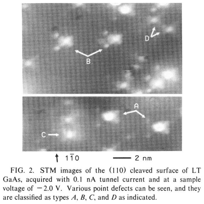
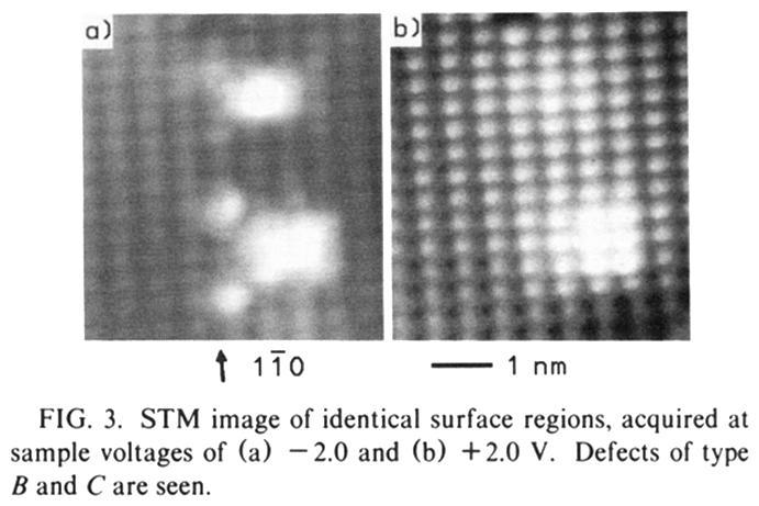
2 VOLUME 71, NUMBER 8 PHYSiCAL REVIEW LETTERS 23 AUGUST M SAMPLE VOLTAGE (V) = E E& (ev) FIG. 1. Tunneling spectra acquired from layers of LT GaAs containing varying amounts of compensating shallow dopants. The valence-band maximum (E ) and conduction-band minimum (E,) are indicated by dashed lines in each spectrum. An intense band of states, arising from arsenic-related defects, appears within the band gap. The states of a bulk arsenic antisite defect are shown in the upper part of the figure, relative to the band edges of spectrum (a). known EL2 level) [6], as shown in the top of Fig. 1 relative to the band edges of spectrum (a). The width of the band we interpret as arising from Coulomb interactions between neighboring arsenic-related defects (for a concentration of 1 x10 cm their average separation is 22 A) and with the shallow dopants [7]. Moving to Figs. 1(b) and 1(c), we see that as shallow acceptors are introduced into the material the Fermi level moves into the band of deep defect states. Thus, these states are donors. For spectrum (c), in which the Fermi level is roughly in the middle of the deep defect band, a distinct minimum in conductance forms at the Fermi level, indicating a gap of about 0.4 ev in the state density. We interpret this gap as arising primarily from the Hubbard U term (0.21 ev in the bulk) [8] separating the two donor levels of the antisite defect, although contributions from the Coulomb gap of the impurity band (0. 1 ev in the bulk) [7] may also be present. In Fig. 2 we show STM images of the p+ LT-GaAs layer. These images are acquired with negative sample bias, so that the background atomic corrugation arises from the As sublattice of the GaAs. Numerous defects are visible in the images, and these defects can be classified into several types as labeled in Fig. 2. The largest apparent defect is type 2, and the next largest is type 8. Note the presence of two distinct satellites around the type 8 defects, and these satellites can be faintly seen around the type 2 defects as well. Other smaller types of defects are labeled C and D in Fig. 2, and most unlabeled defects in the images can be seen to fall within one of &Vo 2 nn FIG. 2. STM images of the (110) cleaved surface of LT GaAs, acquired with 0. 1 na tunnel current and at a sample voltage of 2.0 V. Various point defects can be seen, and they are classified as types 2, 8, C, and D as indicated. these four classes. Images such as those shown in Fig. 2 have been obtained from five samples with various shallow dopant concentrations, each with different probe-tip geometries, and the results for observed defect types and the presence of the satellite features have been reproduced in each case. It is important to note that for imaging of filled states near the band edge as in Fig. 2, the appearance of the defects is completely dominated by tunneling through the deep defect states. Voltage-dependent imaging of the empty states, which do not include contributions from the gap states, reveals a relatively unperturbed Ga sublattice in the vicinity of the defects, as shown in Fig. 3. Thus, the defect images shown in Fig. 2 are, in essence, images of the deep defect states seen in the spectra of Fig. 1. In Fig. 4 we show expanded views of each of the types of defects observed in Fig. 2. A clue to the origin of the difterent types of defects can be obtained by noting the 1 nrn FIG. 3. STM image of identical surface regions, acquired at sample voltages of (a) 2.0 and (b) +2.0 V. Defects of type 8 and C are seen. 1177

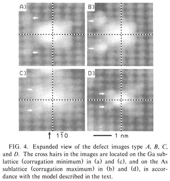
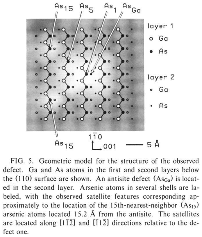
3 VOLUME 71, NUMBER 8 PH YSICAL REVIEW LETTERS 23 AUGUST l 993 As15 I'/ / As As / /r As layer 1 o Ga ~ As layer Ga Z ~ As As t. oo~ 5 A FIG. 4. Expanded view of the defect images type 2, B, C, and D. The cross hairs in the images are located on the Ga sublattice (corrugation minimum) in (a) and (c), and on the As sublattice (corrugation maximum) in (b) and (d), in accordance with the model described in the text. symmetry of the defects relative to the background As sublattice. In particular, the type 4 defects are seen to extend over an even number of rows in the [110] surface direction [e.g., six rows between and including the satellites as indicated by the arrows in Fig. 4(a)l, whereas the type 8 defects extend over an odd number of rows [five rows between and including the satellites as in Fig. 4(b)]. Similarly, the type C and D defects extend over an even and odd number of rows, respectively (satellites are not seen for these defects due to insufticient sensitivity, so the arrows in Fig. 4 simply mark the neighboring unit cells around the defect core). This type of even-odd symmetry is precisely what occurs for a defect on a given lattice site as one moves through consecutive higher-lying planes in the (110) direction. Thus, we interpret all of the observed images as arising from a single type of defect structure in which the defect core is located in dia'ering lattice planes relative to the cleavage plane. This variation is, of course, to be expected for the present case of buik defects in the GaAs. Specifically, the image types 2, 8, C, and D are interpreted as an arsenic-related point defect located 0, 1, 2, or 3 planes (2.0 A spacing) below the (110) cleavage plane. From the observed structure of the type 4 images, the central core of the arsenic-related defect is seen to reside on the Ga sublattice. Given the above interpretation of the images in terms of the depth of the defect core below the cleavage plane, we can construct a geometric model for the defect structure, as shown in Fig. 5. As a reference we choose the observed type 8 image, so that the defect core is in the second layer below the surface. Since the dominant defect in LT GaAs is known to be the arsenic antisite, and the location of this defect on the Ga sublattice is con- FIG. 5. Geometric model for the structure of the observed defect. Ga and As atoms in the first and second layers below the (110) surface are shown. An antisite defect (Aso, ) is located in the second layer. Arsenic atoms in several shells are labeled, with the observed satellite features corresponding approximately to the location of the 15th-nearest-neighbor (As~&) arsenic atoms located 15.2 A from the antisite. The satellites are located along [112] and [112] directions relative to the defect one. sistent with our observations, we place the antisite, Asg in the second layer as shown in Fig. 5. All the defects observed here possess a single (110) mirror plane passing through the central AsG as shown by the horizontal dashed lines in Fig. 4. This is the only symmetry operation present on the (110) surface. If the defects themselves have lower than tetrahedral symmetry, then, assuming they are randomly oriented relative to the surface, a fraction of the observed defects should violate this (110) mirror re[]ection. Even if the defects tend to orient themselves relative to the cleavage plane, we expect for defect complexes with low symmetry that the cleavage procedure will split some of the complexes, leading to a greater diversity of images and spectroscopy than that seen here. We conclude that the defects have tetrahedral symmetry in the bulk. With the central core of the arsenic-related defects consisting of Aso the outstanding question concerning the STM images is the origin of the observed satellites. This is of particular interest for these defects which are responsible for the EL2 level, since they are known to contain a central As~ but considerable controversy surrounds the possibility of additional defects such as interstitial arsenic being located near the antisite defect [8-10]. The possibility that the observed satellites arise from two (or more) additional defects can be excluded on the basis of spatially resolved spectroscopy measurements: Current images acquired at voltages throughout the band gap reveal that the spectrum of states measured over the satellites is basically the same as that acquired over the defect core [11]. Thus, we conclude that the ob- 1178
4 VOLUME 71, NUMBER 8 PH YSICAL REVIEW LETTERS 23 AUGUST 1993 served satellite features are purely electronic features of the defect, arising from tails of the antisite wave function. The observed amplitude of the satellites corresponds to less than 1% of the state-density relative to that at the defect core. The satellite features probably arise from strain-related variations in surface buckling. Similar eff'ects, though not so long range, have been seen in recent computations for Si donors at the GaAs(110) surface [12]. In conclusion, we have used the STM to study the geometric and electronic properties of arsenic-related point defects in LT GaAs. We observe a band of donor states located near E ev arising from the defects, which is close to the energy of the well-known EL2 level in GaAs. The number of observed defects is about 1 x 10 cm, which is the same as the number of EL2- producing defects observed in LT GaAs by infrared adsorption studies [2]. We thus identify our defects as being identical to those which produce EL2 in LT GaAs, the structure which is known to consist primarily of an arsenic antisite [2,8-10]. We find a structure for the defect which is consistent with an isolated antisite in a tetrahedral environment. The possibility of a low symmetry defect complex, in particular an additional arsenic interstitial atom located along a [111] direction [9], is inconsistent with the observed symmetry and spectroscopy of our defects. A more complete understanding of the long range satellite features seen in the STM images may yield additional structural information concerning this EL 2-producing defect. We thank 3. A. Stroscio and H. W. M. Salemink for discussions concerning STM probe-tip preparation and cross-sectional imaging. [1] G. Cox, D. Szynka, U. Poppe, K. H. Graf, K. Urban, C. Kisielowski-Kemmerich, 3. Kriiger, and H. Alexander, Phys. Rev. Lett. 64, 2402 (1990). [2] See, e.g., M. Kaminska and E. R. Weber, Mater. Sci. Forum 83-$7, 1033 (1992), and references therein. [3] H. W. M. Salemink, O. Albrektsen, and P. Koenraad, Phys. Rev. B 45, 6946 (1992). [4] R. M. Feenstra, E. T. Yu, 3. M. Woodall, P. D. Kirchner, C. L. Lin, and G. D. Pettit, Appl. Phys. Lett. 61, 795 (1992). [5] A. Vaterlaus, R. M. Feenstra, P. D. Kirchner, J. M. Woodall, and G. D. Pettit, J. Vac. Sci. Technol. B (to be published). [6] E. R. Weber, H. Ennen, U. Kaufman, J. Windscheif, 3. Schneider, and T. Wosinski, 3. Appl. Phys. 53, 6140 (1982). [7] B. I. Shklovskii and A. L. Efros, Electronic Properties of Doped Semiconductors (Springer-Verlag, Berlin, 1984). The energy scale for Coulomb interactions is e N't /a= ev for our system with dielectric constant of a=12.9 and defect concentration of % =1 & 10 cm. The Coulomb gap is typically twice this value. [8] 3. Dabrowski and M. Schetller, Phys. Rev. B 40, (1989). [9] B. K. Meyer, D. M. Hofmann, J. R. Niklas, and 3.-M. Spaeth, Phys. Rev. B 36, 1332 (1987). [10] M. K. Nissen, A. Villemaire, and M. L. W. Thewalt, Phys. Rev. Lett. 67, 112 (1991). [11]R. M. Feenstra, 3. M. Woodall, and G. D. Pettit (to be published). [12] J. Wang, T. A. Arias, J. D. Joannopoulos, G. W. Turner, and O. L. Alerhand, Phys. Rev. B 47, (1993). 1179
5
6
7
8
Low-temperature Scanning Tunneling Spectroscopy of Semiconductor Surfaces
 Low-temperature Scanning Tunneling Spectroscopy of Semiconductor Surfaces R. M. Feenstra 1 Department of Physics, Carnegie Mellon University, Pittsburgh, Pennsylvania 15213 G. Meyer 2 Paul Drude Institut
Vacancy migration, adatom motion, a.nd atomic bistability on the GaAs(110) surface studied by scanning tunneling microscopy
 surface studied by scanning tunneling microscopy") acancy migration, adatom motion, a.nd atomic bistability on the GaAs(110) surface studied by scanning tunneling microscopy s. Gwo, A. R. Smith, and C. K. Shih Department of Physics, The University of Texas
acancy migration, adatom motion, a.nd atomic bistability on the GaAs(110) surface studied by scanning tunneling microscopy s. Gwo, A. R. Smith, and C. K. Shih Department of Physics, The University of Texas
Scanning tunneling microscopy on unpinned GaN(11 00) surfaces: Invisibility of valence-band states
 surfaces: Invisibility of valence-band states") Scanning tunneling microscopy on unpinned GaN(11 00) surfaces: Invisibility of valence-band states Ph. Ebert, 1, * L. Ivanova, 2 and H. Eisele 2 1 Institut für Festkörperforschung, Forschungszentrum Jülich
Scanning tunneling microscopy on unpinned GaN(11 00) surfaces: Invisibility of valence-band states Ph. Ebert, 1, * L. Ivanova, 2 and H. Eisele 2 1 Institut für Festkörperforschung, Forschungszentrum Jülich
Compositional variations in strain-compensated InGaAsP/InAsP superlattices studied by scanning tunneling microscopy
 Compositional variations in strain-compensated InGaAsP/InAsP superlattices studied by scanning tunneling microscopy B. Grandidier and R. M. Feenstra (a) Department of Physics, Carnegie Mellon University,
Cross-Sectional Scanning Tunneling Microscopy
 Chem. Rev. 1997, 97, 1017 1044 1017 Cross-Sectional Scanning Tunneling Microscopy Edward T. Yu Department of Electrical and Computer Engineering, University of California at San Diego, La Jolla, California
Electronic States of InAs/GaAs Quantum Dots by Scanning Tunneling Spectroscopy
 Electronic States of InAs/GaAs Quantum Dots by Scanning Tunneling Spectroscopy S. Gaan, Guowei He, and R. M. Feenstra Dept. Physics, Carnegie Mellon University, Pittsburgh, PA 15213 J. Walker and E. Towe
Influence of surface states on tunneling spectra of n-type GaAs(110) surfaces
 surfaces") Influence of surface states on tunneling spectra of n-type GaAs(110) surfaces Nobuyuki Ishida, 1 Kazuhisa Sueoka, 1 and R. M. Feenstra 2, * 1 Graduate School of Information Science and Technology, Hokkaido
Influence of surface states on tunneling spectra of n-type GaAs(110) surfaces Nobuyuki Ishida, 1 Kazuhisa Sueoka, 1 and R. M. Feenstra 2, * 1 Graduate School of Information Science and Technology, Hokkaido
Distribution of Nitrogen Atoms in Dilute GaAsN and InGaAsN Alloys studied by Scanning Tunneling Microscopy
 1 Introduction Distribution of Nitrogen Atoms in Dilute GaAsN and InGaAsN Alloys studied by Scanning Tunneling Microscopy H. A. McKay and R. M. Feenstra Department of Physics, Carnegie Mellon University,
Scanning Tunneling Microscopy. how does STM work? the quantum mechanical picture example of images how can we understand what we see?
 Scanning Tunneling Microscopy how does STM work? the quantum mechanical picture example of images how can we understand what we see? Observation of adatom diffusion with a field ion microscope Scanning
K. Sadra, Y. C. Shih, and B. G. Streetman Department of Electrical and Computer Engineering. The University of Texas at Austin. Austin.
 Comparative study of cross-sectional scanning tunneling microscopyl spectroscopy on III-V hetero.. and homostructures: Ultrahigh vacuum-cleaved versus sulfide passivated A. R. Smith and S. Gwo Department
Cross-Section Scanning Tunneling Microscopy of InAs/GaSb Superlattices
 Cross-Section Scanning Tunneling Microscopy of InAs/GaSb Superlattices Cecile Saguy A. Raanan, E. Alagem and R. Brener Solid State Institute. Technion, Israel Institute of Technology, Haifa 32000.Israel
Application of single crystalline tungsten for fabrication of high resolution STM probes with controlled structure 1
 Application of single crystalline tungsten for fabrication of high resolution STM probes with controlled structure 1 A. N. Chaika a, S. S. Nazin a, V. N. Semenov a, V. G. Glebovskiy a, S. I. Bozhko a,b,
arxiv: v1 [cond-mat.dis-nn] 31 Aug 2011
![arxiv: v1 [cond-mat.dis-nn] 31 Aug 2011](/thumbs/94/119863068.jpg "arxiv: v1 [cond-mat.dis-nn] 31 Aug 2011") Suppression of the virtual Anderson transition in a narrow impurity band of doped quantum well structures. N.V. Agrinskaya, V.I. Kozub, and D.S. Poloskin Ioffe Physical-Technical Institute of the Russian
Suppression of the virtual Anderson transition in a narrow impurity band of doped quantum well structures. N.V. Agrinskaya, V.I. Kozub, and D.S. Poloskin Ioffe Physical-Technical Institute of the Russian
Defense Technical Information Center Compilation Part Notice
 UNCLASSIFIED Defense Technical Information Center Compilation Part Notice ADP012911 TITLE: Low Temperature Scanning Tunneling Spectroscopy of Different Individual Impurities on GaAs [110] Surface and in
Direct Observation of Nodes and Twofold Symmetry in FeSe Superconductor
 www.sciencemag.org/cgi/content/full/332/6036/1410/dc1 Supporting Online Material for Direct Observation of Nodes and Twofold Symmetry in FeSe Superconductor Can-Li Song, Yi-Lin Wang, Peng Cheng, Ye-Ping
Pb thin films on Si(111): Local density of states and defects
: Local density of states and defects") University of Wollongong Research Online Australian Institute for Innovative Materials - Papers Australian Institute for Innovative Materials 2014 Pb thin films on Si(111): Local density of states and
University of Wollongong Research Online Australian Institute for Innovative Materials - Papers Australian Institute for Innovative Materials 2014 Pb thin films on Si(111): Local density of states and
Spectroscopy at nanometer scale
 Spectroscopy at nanometer scale 1. Physics of the spectroscopies 2. Spectroscopies for the bulk materials 3. Experimental setups for the spectroscopies 4. Physics and Chemistry of nanomaterials Various
2. Point Defects. R. Krause-Rehberg
 R. Krause-Rehberg 2. Point Defects (F-center in NaCl) 2.1 Introduction 2.2 Classification 2.3 Notation 2.4 Examples 2.5 Peculiarities in Semiconductors 2.6 Determination of Structure and Concentration
Mn in GaAs: from a single impurity to ferromagnetic layers
 Mn in GaAs: from a single impurity to ferromagnetic layers Paul Koenraad Department of Applied Physics Eindhoven University of Technology Materials D e v i c e s S y s t e m s COBRA Inter-University Research
Tunneling spectroscopic analysis of optically active wide band.. gap semiconductors
 Tunneling spectroscopic analysis of optically active wide band.. gap semiconductors D. A Bonnell and G. S. Rohrer") The University of Pennsylvania, Philadelphia, Pennsylvania 19104 R. H. French E. 1. DuPont
Self-compensating incorporation of Mn in Ga 1 x Mn x As
 Self-compensating incorporation of Mn in Ga 1 x Mn x As arxiv:cond-mat/0201131v1 [cond-mat.mtrl-sci] 9 Jan 2002 J. Mašek and F. Máca Institute of Physics, Academy of Sciences of the CR CZ-182 21 Praha
Study of interface asymmetry in InAs GaSb heterojunctions
 Study of interface asymmetry in InAs GaSb heterojunctions M. W. Wang, D. A. Collins, and T. C. McGill T. J. Watson, Sr. Laboratory of Applied Physics, California Institute of Technology, Pasadena, California
Supplementary Information for Solution-Synthesized Chevron Graphene Nanoribbons Exfoliated onto H:Si(100)
") Supplementary Information for Solution-Synthesized Chevron Graphene Nanoribbons Exfoliated onto H:Si(100) Adrian Radocea,, Tao Sun,, Timothy H. Vo, Alexander Sinitskii,,# Narayana R. Aluru,, and Joseph
Supplementary Information for Solution-Synthesized Chevron Graphene Nanoribbons Exfoliated onto H:Si(100) Adrian Radocea,, Tao Sun,, Timothy H. Vo, Alexander Sinitskii,,# Narayana R. Aluru,, and Joseph
Introduction into Positron Annihilation
 Introduction into Positron Annihilation Introduction (How to get positrons? What is special about positron annihilation?) The methods of positron annihilation (positron lifetime, Doppler broadening, ACAR...)
Surface physics, Bravais lattice
 Surface physics, Bravais lattice 1. Structure of the solid surface characterized by the (Bravais) lattice + space + point group lattice describes also the symmetry of the solid material vector directions
Document Version Publisher s PDF, also known as Version of Record (includes final page, issue and volume numbers)
") Controlled charge switching on a single donor with a scanning tunneling microscope Teichmann, K.; Wenderoth, M.; Loth, S.; Ulbrich, R.G.; Garleff, J.K.; Wijnheijmer, A.P.; Koenraad, P.M. Published in:
Controlled charge switching on a single donor with a scanning tunneling microscope Teichmann, K.; Wenderoth, M.; Loth, S.; Ulbrich, R.G.; Garleff, J.K.; Wijnheijmer, A.P.; Koenraad, P.M. Published in:
Spatially resolving density-dependent screening around a single charged atom in graphene
 Supplementary Information for Spatially resolving density-dependent screening around a single charged atom in graphene Dillon Wong, Fabiano Corsetti, Yang Wang, Victor W. Brar, Hsin-Zon Tsai, Qiong Wu,
Defense Technical Information Center Compilation Part Notice
 UNCLASSIFIED Defense Technical Information Center Compilation Part Notice ADP012727 TITLE: Correlated Dopant Distributions in Delta-Doped Layers DISTRIBUTION: Approved for public release, distribution
Cross-sectional scanning tunneling microscopy of InAsSb/InAsP superlattices
 Cross-sectional scanning tunneling microscopy of InAsSb/InAsP superlattices S. L. Zuo and E. T. Yu a) Department of Electrical and Computer Engineering, University of California at San Diego, La Jolla,
Study of semiconductors with positrons. Outlook:
 Study of semiconductors with positrons V. Bondarenko, R. Krause-Rehberg Martin-Luther-University Halle-Wittenberg, Halle, Germany Introduction Positron trapping into defects Methods of positron annihilation
Reflection high energy electron diffraction and scanning tunneling microscopy study of InP(001) surface reconstructions
 surface reconstructions") Reflection high energy electron diffraction and scanning tunneling microscopy study of InP(001) surface reconstructions V.P. LaBella, Z. Ding, D.W. Bullock, C. Emery, and P.M. Thibado Department of Physics,
Reflection high energy electron diffraction and scanning tunneling microscopy study of InP(001) surface reconstructions V.P. LaBella, Z. Ding, D.W. Bullock, C. Emery, and P.M. Thibado Department of Physics,
Quantitative Determination of Nanoscale Electronic Properties of Semiconductor Surfaces by Scanning Tunnelling Spectroscopy
 Quantitative Determination of Nanoscale Electronic Properties of Semiconductor Surfaces by Scanning Tunnelling Spectroscopy R. M. Feenstra 1 and S. Gaan Dept. Physics, Carnegie Mellon Universit Pittsburgh,
Scanning Tunneling Microscopy Studies of the Ge(111) Surface
 Surface") VC Scanning Tunneling Microscopy Studies of the Ge(111) Surface Anna Rosen University of California, Berkeley Advisor: Dr. Shirley Chiang University of California, Davis August 24, 2007 Abstract: This
VC Scanning Tunneling Microscopy Studies of the Ge(111) Surface Anna Rosen University of California, Berkeley Advisor: Dr. Shirley Chiang University of California, Davis August 24, 2007 Abstract: This
Indium incorporation and surface segregation during InGaN growth by molecular beam epitaxy: experiment and theory
 Indium incorporation and surface segregation during InGaN growth by molecular beam epitaxy: experiment and theory Huajie Chen 1,1 R. M. Feenstra 1, J. E. Northrup 2, J. Neugebauer 3, and D. W. Greve 4
Direct observation of a Ga adlayer on a GaN(0001) surface by LEED Patterson inversion. Xu, SH; Wu, H; Dai, XQ; Lau, WP; Zheng, LX; Xie, MH; Tong, SY
 surface by LEED Patterson inversion. Xu, SH; Wu, H; Dai, XQ; Lau, WP; Zheng, LX; Xie, MH; Tong, SY") Title Direct observation of a Ga adlayer on a GaN(0001) surface by LEED Patterson inversion Author(s) Xu, SH; Wu, H; Dai, XQ; Lau, WP; Zheng, LX; Xie, MH; Tong, SY Citation Physical Review B - Condensed
Title Direct observation of a Ga adlayer on a GaN(0001) surface by LEED Patterson inversion Author(s) Xu, SH; Wu, H; Dai, XQ; Lau, WP; Zheng, LX; Xie, MH; Tong, SY Citation Physical Review B - Condensed
Breakdown of cation vacancies into anion vacancy-antisite complexes on III-V semiconductor surfaces
 Breakdown of cation vacancies into anion vacancy-antisite complexes on III-V semiconductor surfaces A. Höglund and S. Mirbt Department of Physics, Uppsala University, Box 530, SE-75121 Uppsala, Sweden
Electronic States of Oxidized GaN(0001) Surfaces
 Surfaces") Electronic States of Oxidized GaN(0001) Surfaces Y. Dong and R. M. Feenstra Dept. Physics, Carnegie Mellon University, Pittsburgh, PA 15213 J. E. Northrup Palo Alto Research Center, 3333 Coyote Hill Road,
Electronic States of Oxidized GaN(0001) Surfaces Y. Dong and R. M. Feenstra Dept. Physics, Carnegie Mellon University, Pittsburgh, PA 15213 J. E. Northrup Palo Alto Research Center, 3333 Coyote Hill Road,
Electronic States of Chemically Treated SiC Surfaces
 Electronic States of Chemically Treated SiC Surfaces Shu Nie and R. M. Feenstra Dept. of Physics, Carnegie Mellon University, Pittsburgh, PA 15213 Y. Ke, R. P. Devaty and W. J. Choyke Dept. of Physics
EECS130 Integrated Circuit Devices
 EECS130 Integrated Circuit Devices Professor Ali Javey 8/30/2007 Semiconductor Fundamentals Lecture 2 Read: Chapters 1 and 2 Last Lecture: Energy Band Diagram Conduction band E c E g Band gap E v Valence
characterization in solids
 Electrical methods for the defect characterization in solids 1. Electrical residual resistivity in metals 2. Hall effect in semiconductors 3. Deep Level Transient Spectroscopy - DLTS Electrical conductivity
Low-temperature tunneling spectroscopy of Ge(111)c( 2 8 ) surfaces
c( 2 8 ) surfaces") Low-temperature tunneling spectroscopy of Ge(111)c( 2 8 ) surfaces R. M. Feenstra 1 and S. Gaan Department of Physics, Carnegie Mellon University, Pittsburgh, Pennsylvania 15213 G. Meyer 2 Paul Drude Institut
Low-temperature tunneling spectroscopy of Ge(111)c( 2 8 ) surfaces R. M. Feenstra 1 and S. Gaan Department of Physics, Carnegie Mellon University, Pittsburgh, Pennsylvania 15213 G. Meyer 2 Paul Drude Institut
Supplementary Figures
 Supplementary Figures Supplementary Figure S1: Calculated band structure for slabs of (a) 14 blocks EuRh2Si2/Eu, (b) 10 blocks SrRh2Si2/Sr, (c) 8 blocks YbRh2Si2/Si, and (d) 14 blocks EuRh2Si2/Si slab;
Crystalline Surfaces for Laser Metrology
 Crystalline Surfaces for Laser Metrology A.V. Latyshev, Institute of Semiconductor Physics SB RAS, Novosibirsk, Russia Abstract: The number of methodological recommendations has been pronounced to describe
Hydrogen termination following Cu deposition on Si(001)
") Hydrogen termination following Cu deposition on Si(001) L. A. Baker, A. R. Laracuente,* and L. J. Whitman Naval Research Laboratory, Washington, DC 20375-5342, USA Received 9 September 2004; published
Hydrogen termination following Cu deposition on Si(001) L. A. Baker, A. R. Laracuente,* and L. J. Whitman Naval Research Laboratory, Washington, DC 20375-5342, USA Received 9 September 2004; published
Lecture 7: Extrinsic semiconductors - Fermi level
 Lecture 7: Extrinsic semiconductors - Fermi level Contents 1 Dopant materials 1 2 E F in extrinsic semiconductors 5 3 Temperature dependence of carrier concentration 6 3.1 Low temperature regime (T < T
Solid Surfaces, Interfaces and Thin Films
 Hans Lüth Solid Surfaces, Interfaces and Thin Films Fifth Edition With 427 Figures.2e Springer Contents 1 Surface and Interface Physics: Its Definition and Importance... 1 Panel I: Ultrahigh Vacuum (UHV)
Review of Semiconductor Fundamentals
 ECE 541/ME 541 Microelectronic Fabrication Techniques Review of Semiconductor Fundamentals Zheng Yang (ERF 3017, email: yangzhen@uic.edu) Page 1 Semiconductor A semiconductor is an almost insulating material,
1 Corresponding author:
 Scanning Tunneling Microscopy Study of Cr-doped GaN Surface Grown by RF Plasma Molecular Beam Epitaxy Muhammad B. Haider, Rong Yang, Hamad Al-Brithen, Costel Constantin, Arthur R. Smith 1, Gabriel Caruntu
Introduction to Semiconductor Physics. Prof.P. Ravindran, Department of Physics, Central University of Tamil Nadu, India
 Introduction to Semiconductor Physics 1 Prof.P. Ravindran, Department of Physics, Central University of Tamil Nadu, India http://folk.uio.no/ravi/cmp2013 Review of Semiconductor Physics Semiconductor fundamentals
Scanning Tunneling Microscopy
 Scanning Tunneling Microscopy Scanning Direction References: Classical Tunneling Quantum Mechanics Tunneling current Tunneling current I t I t (V/d)exp(-Aφ 1/2 d) A = 1.025 (ev) -1/2 Å -1 I t = 10 pa~10na
Supplementary information
 Supplementary information Supplementary Figure S1STM images of four GNBs and their corresponding STS spectra. a-d, STM images of four GNBs are shown in the left side. The experimental STS data with respective
Stripes developed at the strong limit of nematicity in FeSe film
 Stripes developed at the strong limit of nematicity in FeSe film Wei Li ( ) Department of Physics, Tsinghua University IASTU Seminar, Sep. 19, 2017 Acknowledgements Tsinghua University Prof. Qi-Kun Xue,
High resolution STM imaging with oriented single crystalline tips
 High resolution STM imaging with oriented single crystalline tips A. N. Chaika a, *, S. S. Nazin a, V. N. Semenov a, N. N Orlova a, S. I. Bozhko a,b, O. Lübben b, S. A. Krasnikov b, K. Radican b, and I.
The Structure of GaSb Digitally Doped with Mn
 The Structure of GaSb Digitally Doped with Mn G. I. Boishin a,, J. M. Sullivan a,b,,* and L. J. Whitman a,* a Naval Research Laboratory, Washington, DC 20375 b Northwestern University, Evanston, IL 20208
LOW-TEMPERATURE Si (111) HOMOEPITAXY AND DOPING MEDIATED BY A MONOLAYER OF Pb
 HOMOEPITAXY AND DOPING MEDIATED BY A MONOLAYER OF Pb") LOW-TEMPERATURE Si (111) HOMOEPITAXY AND DOPING MEDIATED BY A MONOLAYER OF Pb O.D. DUBON, P.G. EVANS, J.F. CHERVINSKY, F. SPAEPEN, M.J. AZIZ, and J.A. GOLOVCHENKO Division of Engineering and Applied Sciences,
LOW-TEMPERATURE Si (111) HOMOEPITAXY AND DOPING MEDIATED BY A MONOLAYER OF Pb O.D. DUBON, P.G. EVANS, J.F. CHERVINSKY, F. SPAEPEN, M.J. AZIZ, and J.A. GOLOVCHENKO Division of Engineering and Applied Sciences,
Studies of Iron-Based Superconductor Thin Films
 MBE Growth and STM Studies of Iron-Based Superconductor Thin Films Wei Li 1, Canli Song 1,2, Xucun Ma 2, Xi Chen 1*, Qi-Kun Xu 1 State Key Laboratory of Low-Dimensional Quantum Physics, Department of Physics,
2) Atom manipulation. Xe / Ni(110) Model: Experiment:
 Atom manipulation. Xe / Ni(110) Model: Experiment:") 2) Atom manipulation D. Eigler & E. Schweizer, Nature 344, 524 (1990) Xe / Ni(110) Model: Experiment: G.Meyer, et al. Applied Physics A 68, 125 (1999) First the tip is approached close to the adsorbate
2) Atom manipulation D. Eigler & E. Schweizer, Nature 344, 524 (1990) Xe / Ni(110) Model: Experiment: G.Meyer, et al. Applied Physics A 68, 125 (1999) First the tip is approached close to the adsorbate
Introduction to Scanning Tunneling Microscopy
 Introduction to Scanning Tunneling Microscopy C. JULIAN CHEN IBM Research Division Thomas J. Watson Research Center Yorktown Heights, New York New York Oxford OXFORD UNIVERSITY PRESS 1993 CONTENTS List
Scanning probe microscopy of graphene with a CO terminated tip
 Scanning probe microscopy of graphene with a CO terminated tip Andrea Donarini T. Hofmann, A. J. Weymouth, F. Gießibl 7.5.2014 - Theory Group Seminar The sample Single monolayer of graphene Epitaxial growth
Extreme band bending at MBE-grown InAs(0 0 1) surfaces induced by in situ sulphur passivation
 surfaces induced by in situ sulphur passivation") Journal of Crystal Growth 237 239 (2002) 196 200 Extreme band bending at MBE-grown InAs(0 0 1) surfaces induced by in situ sulphur passivation M.J. Lowe a, T.D. Veal a, C.F. McConville a, G.R. Bell b,
Journal of Crystal Growth 237 239 (2002) 196 200 Extreme band bending at MBE-grown InAs(0 0 1) surfaces induced by in situ sulphur passivation M.J. Lowe a, T.D. Veal a, C.F. McConville a, G.R. Bell b,
Surface Studies by Scanning Tunneling Microscopy
 Surface Studies by Scanning Tunneling Microscopy G. Binnig, H. Rohrer, Ch. Gerber, and E. Weibel IBM Zurich Research Laboratory, 8803 Ruschlikon-ZH, Switzerland (Received by Phys. Rev. Lett. on 30th April,
Semiconductor physics I. The Crystal Structure of Solids
 Lecture 3 Semiconductor physics I The Crystal Structure of Solids 1 Semiconductor materials Types of solids Space lattices Atomic Bonding Imperfection and doping in SOLIDS 2 Semiconductor Semiconductors
Electron Energy, E E = 0. Free electron. 3s Band 2p Band Overlapping energy bands. 3p 3s 2p 2s. 2s Band. Electrons. 1s ATOM SOLID.
 Electron Energy, E Free electron Vacuum level 3p 3s 2p 2s 2s Band 3s Band 2p Band Overlapping energy bands Electrons E = 0 1s ATOM 1s SOLID In a metal the various energy bands overlap to give a single
Phase Separation and Magnetic Order in K-doped Iron Selenide Superconductor
 Phase Separation and Magnetic Order in K-doped Iron Selenide Superconductor Wei Li 1, Hao Ding 1, Peng Deng 1, Kai Chang 1, Canli Song 1, Ke He 2, Lili Wang 2, Xucun Ma 2, Jiang-Ping Hu 3, Xi Chen 1, *,
Doping properties of C, Si, and Ge impurities in GaN and AlN
 PHYSICAL REVIEW B VOLUME 56, NUMBER 15 15 OCTOBER 1997-I Doping properties of C, Si, and Ge impurities in GaN and AlN P. Bogusławski Department of Physics, North Carolina State University, Raleigh, North
Imaging of Quantum Confinement and Electron Wave Interference
 : Forefront of Basic Research at NTT Imaging of Quantum Confinement and lectron Wave Interference Kyoichi Suzuki and Kiyoshi Kanisawa Abstract We investigated the spatial distribution of the local density
A semiconductor is an almost insulating material, in which by contamination (doping) positive or negative charge carriers can be introduced.
 positive or negative charge carriers can be introduced.") Semiconductor A semiconductor is an almost insulating material, in which by contamination (doping) positive or negative charge carriers can be introduced. Page 2 Semiconductor materials Page 3 Energy levels
Semiconductor A semiconductor is an almost insulating material, in which by contamination (doping) positive or negative charge carriers can be introduced. Page 2 Semiconductor materials Page 3 Energy levels
k y 2 1 J 1 1 [211] k x [011] E F E (ev) K K-points
![k y 2 1 J 1 1 [211] k x [011] E F E (ev) K K-points](/thumbs/75/72768615.jpg "k y 2 1 J 1 1 [211] k x [011] E F E (ev) K K-points") Pis'ma v ZhETF, vol. 93, iss. 9, pp. 579 { 583 c 2011 May 10 Electronic structure of Ge(111)-(21) surface in the presence of doping atoms. Ab initio analysis of STM data S. V. Savinov 1), S. I. Oreshkin,
Pis'ma v ZhETF, vol. 93, iss. 9, pp. 579 { 583 c 2011 May 10 Electronic structure of Ge(111)-(21) surface in the presence of doping atoms. Ab initio analysis of STM data S. V. Savinov 1), S. I. Oreshkin,
Introduction to Engineering Materials ENGR2000. Dr.Coates
 Introduction to Engineering Materials ENGR2000 Chapter 18: Electrical Properties Dr.Coates 18.2 Ohm s Law V = IR where R is the resistance of the material, V is the voltage and I is the current. l R A
A New Method of Scanning Tunneling Spectroscopy for Study of the Energy Structure of Semiconductors and Free Electron Gas in Metals
 SCANNING Vol. 19, 59 5 (1997) Received April 1, 1997 FAMS, Inc. Accepted May, 1997 A New Method of Scanning Tunneling Spectroscopy for Study of the Energy Structure of Semiconductors and Free Electron
Photon Energy Dependence of Contrast in Photoelectron Emission Microscopy of Si Devices
 Photon Energy Dependence of Contrast in Photoelectron Emission Microscopy of Si Devices V. W. Ballarotto, K. Siegrist, R. J. Phaneuf, and E. D. Williams University of Maryland and Laboratory for Physical
3. Two-dimensional systems
 3. Two-dimensional systems Image from IBM-Almaden 1 Introduction Type I: natural layered structures, e.g., graphite (with C nanostructures) Type II: artificial structures, heterojunctions Great technological
Experimental methods in physics. Local probe microscopies I
 Experimental methods in physics Local probe microscopies I Scanning tunnelling microscopy (STM) Jean-Marc Bonard Academic year 09-10 1. Scanning Tunneling Microscopy 1.1. Introduction Image of surface
Novel materials and nanostructures for advanced optoelectronics
 Novel materials and nanostructures for advanced optoelectronics Q. Zhuang, P. Carrington, M. Hayne, A Krier Physics Department, Lancaster University, UK u Brief introduction to Outline Lancaster University
Quantum Condensed Matter Physics Lecture 12
 Quantum Condensed Matter Physics Lecture 12 David Ritchie QCMP Lent/Easter 2016 http://www.sp.phy.cam.ac.uk/drp2/home 12.1 QCMP Course Contents 1. Classical models for electrons in solids 2. Sommerfeld
Strain-induced electronic property heterogeneity of a carbon nanotube
 PHYSICAL REVIEW B, VOLUME 64, 035419 Strain-induced electronic property heterogeneity of a carbon nanotube D. Tekleab and D. L. Carroll Department of Physics and Astronomy, Clemson University, Kinard Laboratory
Impurities and Electronic Property Variations of Natural MoS 2 Crystal Surfaces
 Supporting Information Impurities and Electronic Property Variations of Natural MoS 2 Crystal Surfaces Rafik Addou 1, *, Stephen McDonnell 1, Diego Barrera 1,2, Zaibing Guo 3, Angelica Azcatl 1, Jian Wang
CITY UNIVERSITY OF HONG KONG. Theoretical Study of Electronic and Electrical Properties of Silicon Nanowires
 CITY UNIVERSITY OF HONG KONG Ë Theoretical Study of Electronic and Electrical Properties of Silicon Nanowires u Ä öä ªqk u{ Submitted to Department of Physics and Materials Science gkö y in Partial Fulfillment
Characterization of Irradiated Doping Profiles. Wolfgang Treberspurg, Thomas Bergauer, Marko Dragicevic, Manfred Krammer, Manfred Valentan
 Characterization of Irradiated Doping Profiles, Thomas Bergauer, Marko Dragicevic, Manfred Krammer, Manfred Valentan Vienna Conference on Instrumentation (VCI) 14.02.2013 14.02.2013 2 Content: Experimental
Mat E 272 Lecture 25: Electrical properties of materials
 Mat E 272 Lecture 25: Electrical properties of materials December 6, 2001 Introduction: Calcium and copper are both metals; Ca has a valence of +2 (2 electrons per atom) while Cu has a valence of +1 (1
Supporting Information
 Supporting Information Defects and Surface Structural Stability of MoTe 2 Under Vacuum Annealing Hui Zhu, Qingxiao Wang, Lanxia Cheng, Rafik Addou, Jiyoung Kim, Moon J. Kim*, Robert M. Wallace* Department
Scanning tunneling microscopy of monoatomic gold chains on vicinal Si(335) surface: experimental and theoretical study
 surface: experimental and theoretical study") phys. stat. sol. (b) 4, No., 33 336 (005) / DOI 10.100/pssb.00460056 Scanning tunneling microscopy of monoatomic gold chains on vicinal Si(335) surface: experimental and theoretical study M. Krawiec *,
phys. stat. sol. (b) 4, No., 33 336 (005) / DOI 10.100/pssb.00460056 Scanning tunneling microscopy of monoatomic gold chains on vicinal Si(335) surface: experimental and theoretical study M. Krawiec *,
Spectroscopy at nanometer scale
 Spectroscopy at nanometer scale 1. Physics of the spectroscopies 2. Spectroscopies for the bulk materials 3. Experimental setups for the spectroscopies 4. Physics and Chemistry of nanomaterials Various
The Effect of Dipole Boron Centers on the Electroluminescence of Nanoscale Silicon p + -n Junctions
 The Effect of Dipole Boron Centers on the Electroluminescence of Nanoscale Silicon p + -n Junctions Nikolay Bagraev a, Leonid Klyachkin a, Roman Kuzmin a, Anna Malyarenko a and Vladimir Mashkov b a Ioffe
C. D. Lee and R. M. Feenstra Dept. Physics, Carnegie Mellon University, Pittsburgh, PA 15213
 Morphology and surface reconstructions of GaN(1 1 00) surfaces C. D. Lee and R. M. Feenstra Dept. Physics, Carnegie Mellon University, Pittsburgh, PA 15213 J. E. Northrup Palo Alto Research Center, 3333
SCANNING PROBE MICROSCOPY OF SEMICONDUCTOR HETEROSTRUCTURES
 Scanning Microscopy Vol. 12, No. 1, 1998 (Pages 43-59) 0891-7035/98$5.00+.25 Scanning Microscopy International, Scanning Chicago probe (AMF microscopy O Hare), IL of 60666 semiconductor USA heterostructures
Nanoprobing of semiconductor heterointerfaces: quantum dots, alloys and diffusion
 INSTITUTE OF PHYSICS PUBLISHING JOURNAL OF PHYSICS D: APPLIED PHYSICS J. Phys. D: Appl. Phys. 37 (24) R163 R178 PII: S22-3727(4)37445- TOPICAL REVIEW Nanoprobing of semiconductor heterointerfaces: quantum
SCIENCE CHINA Physics, Mechanics & Astronomy. Electronic structure and optical properties of N-Zn co-doped -Ga 2 O 3
 SCIENCE CHINA Physics, Mechanics & Astronomy Article April 2012 Vol.55 No.4: 654 659 doi: 10.1007/s11433-012-4686-9 Electronic structure and optical properties of N-Zn co-doped -Ga 2 O 3 YAN JinLiang *
SUPPLEMENTARY INFORMATION
 Simultaneous and coordinated rotational switching of all molecular rotors in a network Y. Zhang, H. Kersell, R. Stefak, J. Echeverria, V. Iancu, U. G. E. Perera, Y. Li, A. Deshpande, K.-F. Braun, C. Joachim,
Surface Transfer Doping of Diamond by Organic Molecules
 Surface Transfer Doping of Diamond by Organic Molecules Qi Dongchen Department of Physics National University of Singapore Supervisor: Prof. Andrew T. S. Wee Dr. Gao Xingyu Scope of presentation Overview
Figure 3.1 (p. 141) Figure 3.2 (p. 142)
 Figure 3.2 (p. 142)") Figure 3.1 (p. 141) Allowed electronic-energy-state systems for two isolated materials. States marked with an X are filled; those unmarked are empty. System 1 is a qualitative representation of a metal;
Figure 3.1 (p. 141) Allowed electronic-energy-state systems for two isolated materials. States marked with an X are filled; those unmarked are empty. System 1 is a qualitative representation of a metal;
Chapter 3 The InAs-Based nbn Photodetector and Dark Current
 68 Chapter 3 The InAs-Based nbn Photodetector and Dark Current The InAs-based nbn photodetector, which possesses a design that suppresses surface leakage current, is compared with both a commercially available
UNIVERSITY OF CALIFORNIA College of Engineering Department of Electrical Engineering and Computer Sciences. EECS 130 Professor Ali Javey Fall 2006
 UNIVERSITY OF CALIFORNIA College of Engineering Department of Electrical Engineering and Computer Sciences EECS 130 Professor Ali Javey Fall 2006 Midterm I Name: Closed book. One sheet of notes is allowed.
Seeing and Manipulating Spin-Spin Interactions at the Single Atomic Level
 Seeing and Manipulating Spin-Spin Interactions at the Single Atomic Level Donghun Lee * Introduction Living in a century of digital and information world, human owe the convenient life to the two modern
Hydrogenated Graphene
 Hydrogenated Graphene Stefan Heun NEST, Istituto Nanoscienze-CNR and Scuola Normale Superiore Pisa, Italy Outline Epitaxial Graphene Hydrogen Chemisorbed on Graphene Hydrogen-Intercalated Graphene Outline
Supporting Information
 Supporting Information Spatially-resolved imaging on photocarrier generations and band alignments at perovskite/pbi2 hetero-interfaces of perovskite solar cells by light-modulated scanning tunneling microscopy
Electrons, Holes, and Defect ionization
 Electrons, Holes, and Defect ionization The process of forming intrinsic electron-hole pairs is excitation a cross the band gap ( formation energy ). intrinsic electronic reaction : null e + h When electrons
Optical Properties of Lattice Vibrations
 Optical Properties of Lattice Vibrations For a collection of classical charged Simple Harmonic Oscillators, the dielectric function is given by: Where N i is the number of oscillators with frequency ω
Lecture 12. study surfaces.
 Lecture 12 Solid Surfaces Techniques to Solid Surfaces. Techniques to study surfaces. Solid Surfaces Molecules on surfaces are not mobile (to large extent) Surfaces have a long-range order (crystalline)
Supplementary information: Topological Properties Determined by Atomic Buckling in Self-Assembled Ultrathin Bi (110)
") Supplementary information: Topological Properties Determined by Atomic Buckling in Self-Assembled Ultrathin Bi (110) Yunhao Lu, *,, Wentao Xu, Mingang Zeng, Guanggeng Yao, Lei Shen, Ming Yang, Ziyu Luo,
Supplementary information: Topological Properties Determined by Atomic Buckling in Self-Assembled Ultrathin Bi (110) Yunhao Lu, *,, Wentao Xu, Mingang Zeng, Guanggeng Yao, Lei Shen, Ming Yang, Ziyu Luo,