Optical Investigation of the Localization Effect in the Quantum Well Structures
|
|
|
- Lucas Lewis
- 5 years ago
- Views:
Transcription
1 Department of Physics Shahrood University of Technology Optical Investigation of the Localization Effect in the Quantum Well Structures Hamid Haratizadeh IPM, SCHOOL OF PHYSICS, JULY
2 2


3 Quantum Well Structures AlGaN GaN Substrate 3
 Recombination Extristic:>>>> with impurity shallow level deep level Intra Band Inter Band")
4 Recombination Processes Intristic:>>> no impurity 1-Band to Band Recombination 2-Free Exciton (FE) Recombination Extristic:>>>> with impurity shallow level deep level Intra Band Inter Band 4
 Hexagonal wurtzite structure Wurtzite is thermodynamically stable")
 E g (AlN)=6.20 ev (P. B. Perry et al.")
5 III-Nitride Nitrides s Semiconductors (a) Cubic zincblende structure (b) Hexagonal wurtzite structure Wurtzite is thermodynamically stable for bulk AlN, GaN and InN. E g (GaN)=3.43 ev (Bo Monemar 1974) E g (AlN)=6.20 ev (P. B. Perry et al. 1978) E g (InN)= ev (J. Wu et al. 2002) 5

6 6
7 Polarization Fields Piezoelectric polarization appears in the presence of strain Lattice mismatch strain Ppz = 2εxx( e31 e33c13 / C33) Thermal strain Along the [0001] direction (Cmn is elastic tensor and εxx is in-plane strain) Spontaneous polarization exists in polar semiconductors with a wurtzite or lower symmetry crystal structure Fixed direction along the [0001] c-axis in the wurtzite lattice In the Al x In y Ga 1-x-y N alloy systems (Vegard-like rule): P SP ( x, y) = xp + yp + (1 x AlN SP InN SP y) P GaN SP The energy bands are tilted and carriers are localized at the opposite interfaces The reduction E of the recombination energy (QCSE) 7

8 Effect of the Polarization Fields on Carrier Localization The in-plane extension of the hole wave function is smaller than the average Al-Al distance in barriers. Moreover, both electron and hole envelope functions are pushed apart from each other by the electric field. M.Gallart et. al. Physica. Status Solidi A 180, 127 (2000) 8
9 Confirmation of the Localization Effect by the Transient PL Above the Mott density, a decrease of the decay time should be expected, but an almost similar decay time was measured for all samples. In the heavily Si-doped samples: free electrons-to-localized holes and an almost constant decay time over the PL spectrum is evidence for the dominant role played by the localized holes. Time Decay (ps) 700 Undoped (a) PL Intensity (arb. units) Decay Time (ps) 700 Si: cm -3 (b) PL Intensity (arb. units) Photon Energy (ev) Photon Energy (ev) 9
10 MQW samples with Different Well Width T=2 K 45 Å 30 Å 15 Å Residual doping ~ cm Å splitting 10 mev FWHM ~ 15 mev 30 Å FWHM ~ 25 mev 45 Å splitting 25 mev FWHM ~ 20 mev PL Intensity (log scale) LO (45 Å) LO (30 Å) 2nd LO (15 Å) Photon Energy (ev) Well width fluctuation by 2 ML. The main broadening mechanism is the well width fluctuation. The hole localization at lower interface of the QW determines the radiative process at low temperature in terms of spectral shape, line width. 10
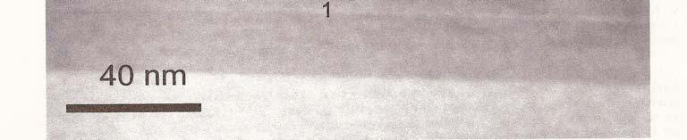
 to produce chemical distribution profiles, using inelastically scattered electrons with")

 GaN/AlGaN-MQW 45 Å, 2 K (c) 3.44 3.46 3.48 3.50 3.52 3.54 3.56 3.58 3.60 Photon energy (ev) 3.46 3.48 3.50 3.52 3.54 3.56 3.58 3.60 3.")
11 PL Mapping PL intensity (arb. units) A cross-section TEM image of the undoped 4.5 nm wide well sample. Energy-filtered TEM (EFTEM) to produce chemical distribution profiles, using inelastically scattered electrons with energy-losses characteristic of the specific Ga and Al elemental species. The EELS study was used to investigate the variation in the Al concentration between the wells with a near nanometer resolution. AlGaN-MQW 30 Å, 2 K (b) PL Intensity (arb. units) AlGaN-MQW 15 Å, 2 K (a) PL Intensity (arb. units) GaN/AlGaN-MQW 45 Å, 2 K (c) Photon energy (ev) Photon energy (ev) Photon energy (ev) 11
12 Ternary III-V-N Structures Diluted N-containing III-V ternary or quaternary semiconductor alloys GaNAs InAsN InPN GaPN Quaternary Ultradilute Nitrogen Concentration: 0.01 < x < 0.1 % Intermediate Nitrogen Concentration: 0.1 < x < 2 % High Nitrogen Concentration: 2 < x < 5 % InGaNP InGaNAs 12


 Multi-Junction")
13 Applications IR Diode Laser for Optical Fibers Communications Vertical Cavity Surface Emitting Laser (VCSEL) Multi-Junction Solar Cells 13
14 Adding N to InGaAs Creating of fluctuations localized Center Large Band-Gap Bowing Increasing of Effective Mass Reduction of Band-Gap Large Band Offset in CB InGaAs InGaNAs 14
15 Band Anticrossing model Splitting of CB into two Subband ( E +, E - ) Reduction of Fundamental Band-gap I. A. Buyanova et al,. Nitride Semiconductor. Research. (2001) & C. Skierbiszewski et al, Appl. Phys. Lett. 76, 2409 (2000) 15
16 Effect of N on the Band Gap, FWHM and PL Intensity of In x Ga 1-x N y As 1-y SQW Normalized PL Intensity(arb.units) In x Ga 1-x N y As 1-y T=150 K ev ev ev P=25 mw (2) x=0.30 y= (1) x=0.354 (3) y= x=0.37 y=0.006 Normalized PL Intensity(arb.units) In x Ga 1-x N y As 1-y T=2 K P=25 mw (3) X=0.37 y= ev ev ev (2) X=0.30 y= (1) X=0.354 y= Energy(ev) Energy(ev) samples FWHM (mev) (T=2K) mev decrease of FWHM (mev) (T=150K) band-gap per %1 N 16
17 The Role of N on the Exciton Localization E( g) αt 2 = E(0) β + T α = β = 347 K 4 ev / K Normalized Intensity (arb.units) In 0.36 GaN As SQW Exc. power=25mw T=10 K T=25 K T=33 K T=40 K T=45 K T=50 K T=55 T=60 K T=70 K T=80 K T=90 K T=110 K T=130 K T=150 K T=220 K T=300 K Energy(ev) 17
18 The Role of N on the Exciton Localization In GaN As/GaAs In 0.3 SQW GaN As/GaAs MQW In 0.36 GaN As/GaAs SQW PL Intensity(arb.units) In GaN As/GaAs SQW Different Excitation Intensity T=2 K ev PL Intensity(arb.units) P=40 mw ev p=10 mw ev P=4 mw 1.00 ev p=27 mw p=5 mw 0.99 ev In 0.36 GaN As SQW Different Excitation Intensity T=2 K In GaN As MQW Different Excitation Intensity T=2 K PL Intensity(arb.units) P=5 mw P=0.5 mw p=27 mw P=10 mw ev ev 1.001eV ev Energy (ev) Energy(eV) Energy (ev) 18

!")
19 InGaNAs Suitable for optoelectronic application Optical devices and lasers with long wavelength (1300 nm & 1550 nm) Quantum structures Why Annealing? Adding N to InGaAs (less than few percent) Increase optical efficiency Advantage: Red shift the energy emission to close to the interest wavelength Disadvantage: Increase nonradiative centers (Decrease the Optical Efficiency)! Low temperature growth and non-equilibrium condition Thermal Annealing Increase defect and nonradiative centers Improvement the optical efficiency 19
20 Annealing Processes Series 1: In x Ga 1-x N y As 1-y /GaAs Single Quantum Well (SQW) Substrate: undoped (001) oriented GaAs Buffer: 300 nm undoped GaAs Cap Layer: 100 nm undoped GaAs Well Thickness: 7 nm In Content (x) = 35.4% N Content (y) = 0.36% 100nm GaAs Cap Layer 7nm InGaNAs Growth Technique: HVPE Growth Temperature: 495 c Annealing Temperature: 900 c Annealing Time: 0, 5, 15 and 30 seconds 300nm GaAs Buffer Layer Substrate GaAs (oo1) GaAs GaAs 20
21 Annealing Processes 1A, 1B, 1C and 1D Normalized PL Intensity (arb. un.) InGaNAs/GaAs SQW 1A, 1B, 1C, 1D 2 k, 27 mw RTA (30 Second) RTA (15 Second) 1A 1B 1D 1C RTA (5 Second) As Grown Photon Energy (ev) FWHM (mev) Annealing Time (Second) Peak Position (ev) Annealing Time (Second) 21
22 Annealing Processes Series 2: In x Ga 1-x N y As 1-y /GaAs Single Quantum Well (SQW) Substrate: undoped (001)Oriented GaAs Buffer: 300 nm undoped GaAs Cap Layer: 100 nm undoped GaAs Well Thickness: 7.2 nm In Content (x) = 37% N Content (y) = 0.59% 100nm GaAs Cap Layer 7.2nm InGaNAs Growth Technique: HVPE Growth Temperature: 495 c Annealing Temperature: 900 c Annealing Time: 0, 5, 15 and 30 seconds 300nm GaAs Buffer Layer Substrate GaAs (oo1) 22
23 Annealing Time vs. N content 1A, 1B, 1C, 1D and FWHM (mev) 2A, 2B, 2C, 2D 40 In Ga N As SQW (square) In 0.37 Ga 0.63 N As SQW (circle) T=2K, 25mW PL Intensity(arb. unit) In 0.37 Ga 0.63 N As A, 2B, 2C, 2D Solid Symbol In Ga N As A, 1B, 1C, 1D Open Symbol 30 sec RTA 15 sec. RTA 5 sec. RTA Annealing Time (Second) as grown Photon Energy (ev) 23
24 Series 3: In x Ga 1-x N y As 1-y /GaAs Multi Quantum Well (MQW) Substrate: undoped (001)Oriented GaAs Buffer: GaAs Cap Layer: 50 nm undoped GaAs Well Thickness: 5.7 nm Barrier Thickness: 19.3 nm In Content (x) = 30% N Content (y) = 1.5% Growth Technique: MOVPE (520 c) Thermal Annealing Processes: Well Barrier 50nm GaAs Cap Layer 5.7nm InGaNAs 19.3nm GaAs 5.7nm InGaNAs 19.3nm GaAs 5.7nm InGaNAs 19.3nm GaAs 5.7nm InGaNAs 19.3nm GaAs 5.7nm InGaNAs GaAs Substrate GaAs (oo1) Rapid Thermal Annealing (RTA) at N 2 atmosphere and 650 c for 15 seconds. Reactor Annealing (R) at H 2 + AsH 3 and 650 c for 30 minuets. 24
25 1A, 1C,and 3A, 3B 1A : as-grown 1C : RTA at 900 c for 15 s InGaNAs/GaAs SQW As grown 15s RTA PL Intensity(arb. unit) 1A 1C FWHM (mev) A : as-grown 80 PL Intensity (a.u.) Photon Energy(ev) 60 3B : RTA at 650 c and N 40 2 atmosphere for 15 s 20 as-grown Annealing Temperature ('c) 0.01 as-grown Annealing Temperature ('c) 3B x = 34%, y = 1% Growth by MOVPE at 510 c Annealing Time : 10 min 25
26 Multi Thermal Annealing Processes 3A, 3B, 3C and 3D In 0.3 GaN As/GaAs MQW T=2K, Power Exc.=40 mw RTA+R+RTA PL Intensity (arb. units) As grown As grown RTA RTA+R RTA+R+RTA * 100 RTA RTA+R Photon Energy (ev) InGaNAs/GaAs MQW T=2K, Power Exc.=4 mw RTA + R + RTA PL Intensity (arb. units) As grown As grown RTA RTA+R RTA+R+RTA 100 RTA RTA + R Photon Energy (ev) 26
27 Multiple Thermal Annealing Processes 3A PL Intensity (arb-unit) As grown (3A) T=2K 40 mw 2 mw PL Intensity (arb-unit) RTA (3B) T=2K 40 mw 4 mw 3B Photon Energy (ev) Photon Energy (ev) 3C PL Intensity (arb-unit) RTA+R (3C) T=2K 40 mw 4 mw PL Intensity (arb-unit) RTA+R+RTA (3D) T=2K 40 mw 4 mw 3D Photon Energy (ev) Photon Energy (ev) 27


28 Structural Changes Ga-As : 2.45 Å In-N : 2.14 Å Ga-N : 1.95 Å As grown Annealed 28
29 Conclusions: Adding Nitrogen to InGaAs Reduction of band-gap (Long Wavelength (IR region)). Increasing Localized Center due to Potential fluctuations Asymmetry of PL spectra S-shape behavior of peak position of PL spectra Decrease Optical Efficiency by Increase in non-radiative Centers. Thermal annealing. Improvement the Optical Efficiency by Suitable Thermal annealing Changes in N Surrounding from Ga4 -N to Ga3In-N Causes Reduction of Strain and Potential Fluctuation. Increases Optical Efficiency Thermal annealing temperature optimum is around c To avoid escaping of nitrogen from compound during annealing, the samples should be annealed in presence of N 2 gas. 29
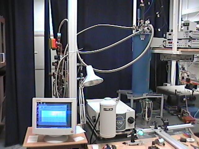
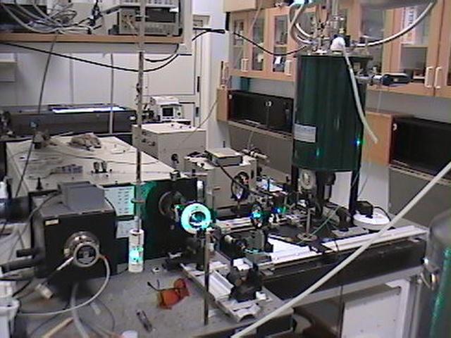
30 Photoluminescence (PL) Setup 30

 ss GaAs InAs GaAs p s pp ss s p Wetting Layer QD x50")
31 Excitation Laser Microscope Objective InAs QDs ~5 nm ~10 µm ~1.5 µm ~35 nm GaAs Detection Energy (ev) PL Intensity (arb. units) ss GaAs InAs GaAs p s pp ss s p Wetting Layer QD x50 E pp - E ss = 30 mev GaAs x50 pp (T = 4 K) 31
32 PL spectra GaN ev Normalized PL Intensity (arb. units) ev ev ev Photon Energy (ev) Undoped Barrier doped Dual doped Well doped Normalized PL Intensity (arb. units) Si: Barrier doped T=2 K ev ev ev ev Undoped Low-doped ( cm -3 ) Medium-doped ( cm -3 ) High-doped ( cm -3 ) Photon Energy (ev) 32
33 PhotoLuminescence Setup Time-Resolved PL Setup 4 µs 200 fs 33
 Intensity Intensity 0.0 1.5 Wavelength 0 500 1000 1500 2000 Time 34")
34 (a) Undoped PL Intensity (arb. units) 50 ps 100 ps 150 ps 200 ps 300 ps 400 ps 500 ps 600 ps Photon Energy (ev) Intensity Intensity Wavelength Time 34
Luminescence basics. Slide # 1
 Luminescence basics Types of luminescence Cathodoluminescence: Luminescence due to recombination of EHPs created by energetic electrons. Example: CL mapping system Photoluminescence: Luminescence due to
Structural and Optical Properties of III-III-V-N Type
 i Structural and Optical Properties of III-III-V-N Type Alloy Films and Their Quantum Wells ( III-III-V- N 型混晶薄膜および量子井戸の構造的および光学的性質 ) This dissertation is submitted as a partial fulfillment of the requirements
Temperature Dependent Optical Band Gap Measurements of III-V films by Low Temperature Photoluminescence Spectroscopy
 Temperature Dependent Optical Band Gap Measurements of III-V films by Low Temperature Photoluminescence Spectroscopy Linda M. Casson, Francis Ndi and Eric Teboul HORIBA Scientific, 3880 Park Avenue, Edison,
Emission Spectra of the typical DH laser
 Emission Spectra of the typical DH laser Emission spectra of a perfect laser above the threshold, the laser may approach near-perfect monochromatic emission with a spectra width in the order of 1 to 10
Introduction to Optoelectronic Device Simulation by Joachim Piprek
 NUSOD 5 Tutorial MA Introduction to Optoelectronic Device Simulation by Joachim Piprek Outline:. Introduction: VCSEL Example. Electron Energy Bands 3. Drift-Diffusion Model 4. Thermal Model 5. Gain/Absorption
Widely Tunable and Intense Mid-Infrared PL Emission from Epitaxial Pb(Sr)Te Quantum Dots in a CdTe Matrix
Te Quantum Dots in a CdTe Matrix") Widely Tunable and Intense Mid-Infrared PL Emission from Epitaxial Pb(Sr)Te Quantum Dots in a Matrix S. Kriechbaumer 1, T. Schwarzl 1, H. Groiss 1, W. Heiss 1, F. Schäffler 1,T. Wojtowicz 2, K. Koike 3,
Widely Tunable and Intense Mid-Infrared PL Emission from Epitaxial Pb(Sr)Te Quantum Dots in a Matrix S. Kriechbaumer 1, T. Schwarzl 1, H. Groiss 1, W. Heiss 1, F. Schäffler 1,T. Wojtowicz 2, K. Koike 3,
Self-Assembled InAs Quantum Dots
 Self-Assembled InAs Quantum Dots Steve Lyon Department of Electrical Engineering What are semiconductors What are semiconductor quantum dots How do we make (grow) InAs dots What are some of the properties
Three-Dimensional Silicon-Germanium Nanostructures for Light Emitters and On-Chip Optical. Interconnects
 Three-Dimensional Silicon-Germanium Nanostructures for Light Emitters and On-Chip Optical eptember 2011 Interconnects Leonid Tsybeskov Department of Electrical and Computer Engineering New Jersey Institute
Ultrafast single photon emitting quantum photonic structures. based on a nano-obelisk
 Ultrafast single photon emitting quantum photonic structures based on a nano-obelisk Je-Hyung Kim, Young-Ho Ko, Su-Hyun Gong, Suk-Min Ko, Yong-Hoon Cho Department of Physics, Graduate School of Nanoscience
solidi current topics in solid state physics InAs quantum dots grown by molecular beam epitaxy on GaAs (211)B polar substrates
B polar substrates") solidi status physica pss c current topics in solid state physics InAs quantum dots grown by molecular beam epitaxy on GaAs (211)B polar substrates M. Zervos1, C. Xenogianni1,2, G. Deligeorgis1, M. Androulidaki1,
solidi status physica pss c current topics in solid state physics InAs quantum dots grown by molecular beam epitaxy on GaAs (211)B polar substrates M. Zervos1, C. Xenogianni1,2, G. Deligeorgis1, M. Androulidaki1,
GeSi Quantum Dot Superlattices
 GeSi Quantum Dot Superlattices ECE440 Nanoelectronics Zheng Yang Department of Electrical & Computer Engineering University of Illinois at Chicago Nanostructures & Dimensionality Bulk Quantum Walls Quantum
Novel materials and nanostructures for advanced optoelectronics
 Novel materials and nanostructures for advanced optoelectronics Q. Zhuang, P. Carrington, M. Hayne, A Krier Physics Department, Lancaster University, UK u Brief introduction to Outline Lancaster University
Intraband emission of GaN quantum dots at λ =1.5 μm via resonant Raman scattering
 Intraband emission of GaN quantum dots at λ =1.5 μm via resonant Raman scattering L. Nevou, F. H. Julien, M. Tchernycheva, J. Mangeney Institut d Electronique Fondamentale, UMR CNRS 8622, University Paris-Sud
Stimulated Emission Devices: LASERS
 Stimulated Emission Devices: LASERS 1. Stimulated Emission and Photon Amplification E 2 E 2 E 2 hυ hυ hυ In hυ Out hυ E 1 E 1 E 1 (a) Absorption (b) Spontaneous emission (c) Stimulated emission The Principle
Electron leakage effects on GaN-based light-emitting diodes
 Opt Quant Electron (2010) 42:89 95 DOI 10.1007/s11082-011-9437-z Electron leakage effects on GaN-based light-emitting diodes Joachim Piprek Simon Li Received: 22 September 2010 / Accepted: 9 January 2011
Optical Gain Analysis of Strain Compensated InGaN- AlGaN Quantum Well Active Region for Lasers Emitting at nm
 Optical Gain Analysis of Strain Compensated InGaN- AlGaN Quantum Well Active Region for Lasers Emitting at 46-5 nm ongping Zhao, Ronald A. Arif, Yik-Khoon Ee, and Nelson Tansu ±, Department of Electrical
Resonantly Excited Time-Resolved Photoluminescence Study of Self-Organized InGaAs/GaAs Quantum Dots
 R. Heitz et al.: PL Study of Self-Organized InGaAs/GaAs Quantum Dots 65 phys. stat. sol. b) 221, 65 2000) Subject classification: 73.61.Ey; 78.47.+p; 78.55.Cr; 78.66.Fd; S7.12 Resonantly Excited Time-Resolved
Detection of NRR Centers in InGaAs/AlGaAs HEMTs: Two-Wavelength Excited Photoluminescence Studies
 Global Science and Technology Journal Vol. 1. No. 1. July 2013 Issue. Pp.1-11 Detection of NRR Centers in InGaAs/AlGaAs HEMTs: Two-Wavelength Excited Photoluminescence Studies A. Z. M. Touhidul Islam 1,
Electronic and Optoelectronic Properties of Semiconductor Structures
 Electronic and Optoelectronic Properties of Semiconductor Structures Jasprit Singh University of Michigan, Ann Arbor CAMBRIDGE UNIVERSITY PRESS CONTENTS PREFACE INTRODUCTION xiii xiv 1.1 SURVEY OF ADVANCES
Investigation of Optical Nonlinearities and Carrier Dynamics in In-Rich InGaN Alloys
 Vol. 113 (2008) ACTA PHYSICA POLONICA A No. 3 Proceedings of the 13th International Symposium UFPS, Vilnius, Lithuania 2007 Investigation of Optical Nonlinearities and Carrier Dynamics in In-Rich InGaN
Spin Dynamics in Single GaAs Nanowires
 1 Dr. Max Mustermann Referat Kommunikation & Marketing Verwaltung Spin Dynamics in Single GaAs Nanowires F. Dirnberger, S. Furthmeier, M. Forsch, A. Bayer, J. Hubmann, B. Bauer, J. Zweck, E. Reiger, C.
ANTIMONY ENHANCED HOMOGENEOUS NITROGEN INCORPORATION INTO GaInNAs FILMS GROWN BY ATOMIC HYDROGEN-ASSISTED MOLECULAR BEAM EPITAXY
 ANTIMONY ENHANCED HOMOGENEOUS NITROGEN INCORPORATION INTO GaInNAs FILMS GROWN BY ATOMIC HYDROGEN-ASSISTED MOLECULAR BEAM EPITAXY Naoya Miyashita 1, Nazmul Ahsan 1, and Yoshitaka Okada 1,2 1. Research Center
Electron Energy, E E = 0. Free electron. 3s Band 2p Band Overlapping energy bands. 3p 3s 2p 2s. 2s Band. Electrons. 1s ATOM SOLID.
 Electron Energy, E Free electron Vacuum level 3p 3s 2p 2s 2s Band 3s Band 2p Band Overlapping energy bands Electrons E = 0 1s ATOM 1s SOLID In a metal the various energy bands overlap to give a single
Luminescence Process
 Luminescence Process The absorption and the emission are related to each other and they are described by two terms which are complex conjugate of each other in the interaction Hamiltonian (H er ). In an
interband transitions in semiconductors M. Fox, Optical Properties of Solids, Oxford Master Series in Condensed Matter Physics
 interband transitions in semiconductors M. Fox, Optical Properties of Solids, Oxford Master Series in Condensed Matter Physics interband transitions in quantum wells Atomic wavefunction of carriers in
Fabrication of Efficient Blue Light-Emitting Diodes with InGaN/GaN Triangular Multiple Quantum Wells. Abstract
 Fabrication of Efficient Blue Light-Emitting Diodes with InGaN/GaN Triangular Multiple Quantum Wells R. J. Choi, H. W. Shim 2, E. K. Suh 2, H. J. Lee 2, and Y. B. Hahn,2, *. School of Chemical Engineering
III-V nanostructured materials synthesized by MBE droplet epitaxy
 III-V nanostructured materials synthesized by MBE droplet epitaxy E.A. Anyebe 1, C. C. Yu 1, Q. Zhuang 1,*, B. Robinson 1, O Kolosov 1, V. Fal ko 1, R. Young 1, M Hayne 1, A. Sanchez 2, D. Hynes 2, and
Room-temperature continuous-wave operation of GaInNAs/GaAs quantum dot laser with GaAsN barrier grown by solid source molecular beam epitaxy
 Room-temperature continuous-wave operation of GaInNAs/GaAs quantum dot laser with GaAsN barrier grown by solid source molecular beam epitaxy Z. Z. Sun 1, S. F. Yoon 1,2, K. C. Yew 1, and B. X. Bo 1 1 School
Course overview. Me: Dr Luke Wilson. The course: Physics and applications of semiconductors. Office: E17 open door policy
 Course overview Me: Dr Luke Wilson Office: E17 open door policy email: luke.wilson@sheffield.ac.uk The course: Physics and applications of semiconductors 10 lectures aim is to allow time for at least one
(b) Spontaneous emission. Absorption, spontaneous (random photon) emission and stimulated emission.
 Spontaneous emission. Absorption, spontaneous (random photon) emission and stimulated emission.") Lecture 10 Stimulated Emission Devices Lasers Stimulated emission and light amplification Einstein coefficients Optical fiber amplifiers Gas laser and He-Ne Laser The output spectrum of a gas laser Laser
Lecture 10 Stimulated Emission Devices Lasers Stimulated emission and light amplification Einstein coefficients Optical fiber amplifiers Gas laser and He-Ne Laser The output spectrum of a gas laser Laser
Multiband GaN/AlGaN UV Photodetector
 Vol. 110 (2006) ACTA PHYSICA POLONICA A No. 2 Proceedings of the XXXV International School of Semiconducting Compounds, Jaszowiec 2006 Multiband GaN/AlGaN UV Photodetector K.P. Korona, A. Drabińska, K.
Semiconductor Quantum Dot Nanostructures and their Roles in the Future of Photonics
 550 Brazilian Journal of Physics, vol. 34, no. 2B, June, 2004 Semiconductor Quantum Dot Nanostructures and their Roles in the Future of Photonics S. Fafard, K. Hinzer, and C. N. Allen Institute for Microstructural
ISSN Review. Progress to a Gallium-Arsenide Deep-Center Laser
 Materials 2009, 2, 1599-1635; doi:10.3390/ma2041599 OPEN ACCESS materials ISSN 1996-1944 www.mdpi.com/journal/materials Review Progress to a Gallium-Arsenide Deep-Center Laser Janet L. Pan Yale University,
Exciton spectroscopy
 Lehrstuhl Werkstoffe der Elektrotechnik Exciton spectroscopy in wide bandgap semiconductors Lehrstuhl Werkstoffe der Elektrotechnik (WW6), Universität Erlangen-Nürnberg, Martensstr. 7, 91058 Erlangen Vortrag
Physics and Material Science of Semiconductor Nanostructures
 Physics and Material Science of Semiconductor Nanostructures PHYS 570P Prof. Oana Malis Email: omalis@purdue.edu Course website: http://www.physics.purdue.edu/academic_programs/courses/phys570p/ 1 Introduction
ECE236A Semiconductor Heterostructure Materials Group III Nitride Semiconductors Lecture 17, Nov. 30, 2017
 ECE236A Semiconductor Heterostructure Materials Group III Nitride Semiconductors Lecture 17, Nov. 30, 2017 Spontaneous and Piezoelectric Polarization Effects on 2DEG in HFETs Effects of Polarization on
InGaAs-AlAsSb quantum cascade lasers
 InGaAs-AlAsSb quantum cascade lasers D.G.Revin, L.R.Wilson, E.A.Zibik, R.P.Green, J.W.Cockburn Department of Physics and Astronomy, University of Sheffield, UK M.J.Steer, R.J.Airey EPSRC National Centre
De De. De M Q fix = const PR R/R Intensity (arb. inits) Energy (ev) a) b)
 Energy (ev) a) b)") PIEZOELECTRIC EFFECTS IN GaInN/GaN HETEROSTRUCTURES AND QUANTUM WELLS C. WETZEL, T. TAKEUCHI, S. YAMAGUCHI, H. KATO, H. AMANO, and I. AKASAKI High Tech Research Center, Meijo University, 1-501 Shiogamaguchi,
PIEZOELECTRIC EFFECTS IN GaInN/GaN HETEROSTRUCTURES AND QUANTUM WELLS C. WETZEL, T. TAKEUCHI, S. YAMAGUCHI, H. KATO, H. AMANO, and I. AKASAKI High Tech Research Center, Meijo University, 1-501 Shiogamaguchi,
Optical properties of wurtzite and zinc-blende GaNÕAlN quantum dots
 Optical properties of wurtzite and zinc-blende GaNÕAlN quantum dots Vladimir A. Fonoberov a) and Alexander A. Balandin b) Nano-Device Laboratory, Department of Electrical Engineering, University of California
Nonlinear Elasticity in Wurtzite GaN/AlN Planar Superlattices and Quantum Dots
 Vol. 108 (2005) ACTA PHYSICA POLONICA A No. 5 Proceedings of the XXXIV International School of Semiconducting Compounds, Jaszowiec 2005 Nonlinear Elasticity in Wurtzite GaN/AlN Planar Superlattices and
Potential and Carrier Distribution in AlGaN Superlattice
 Vol. 108 (2005) ACTA PHYSICA POLONICA A No. 4 Proceedings of the XXXIV International School of Semiconducting Compounds, Jaszowiec 2005 Potential and Carrier Distribution in AlGaN Superlattice K.P. Korona,
Investigation of the formation of InAs QD's in a AlGaAs matrix
 10th Int. Symp. "Nanostructures: Physics and Technology" St Petersburg, Russia, June 17-21, 2002 2002 IOFFE Institute NT.16p Investigation of the formation of InAs QD's in a AlGaAs matrix D. S. Sizov,
Optical and Terahertz Characterization of Be-Doped GaAs/AlAs Multiple Quantum Wells
 Vol. 107 (2005) ACTA PHYSICA POLONICA A No. 2 Proceedings of the 12th International Symposium UFPS, Vilnius, Lithuania 2004 Optical and Terahertz Characterization of Be-Doped GaAs/AlAs Multiple Quantum
Carrier Loss Analysis for Ultraviolet Light-Emitting Diodes
 Carrier Loss Analysis for Ultraviolet Light-Emitting Diodes Joachim Piprek, Thomas Katona, Stacia Keller, Steve DenBaars, and Shuji Nakamura Solid State Lighting and Display Center University of California
Supplementary Information for
 Supplementary Information for Multi-quantum well nanowire heterostructures for wavelength-controlled lasers Fang Qian 1, Yat Li 1 *, Silvija Gradečak 1, Hong-Gyu Park 1, Yajie Dong 1, Yong Ding 2, Zhong
Single Photon Generation & Application
 Single Photon Generation & Application Photon Pair Generation: Parametric down conversion is a non-linear process, where a wave impinging on a nonlinear crystal creates two new light beams obeying energy
1. Binary III-V compounds 2 p From which atoms are the 16 binary III-V compounds formed?...column III B, Al, Ga and In...column V N, P, As and Sb...
 PROBLEMS part B, Semiconductor Materials. 2006 1. Binary III-V compounds 2 p From which atoms are the 16 binary III-V compounds formed?...column III B, Al, Ga and In...column V N, P, As and Sb... 2. Semiconductors
Chapter 5. Semiconductor Laser
 Chapter 5 Semiconductor Laser 5.0 Introduction Laser is an acronym for light amplification by stimulated emission of radiation. Albert Einstein in 1917 showed that the process of stimulated emission must
Simulation of GaN-based Light-Emitting Devices
 Simulation of GaN-based Light-Emitting Devices Joachim Piprek Solid-State Lighting and Display Center Materials Department, College of Engineering University of California, Santa Barbara, CA 93106 piprek@ieee.org
ELECTRONIC STRUCTURE OF InAs/GaAs/GaAsSb QUANTUM DOTS
 ELECTRONIC STRUCTURE OF InAs/GaAs/GaAsSb QUANTUM DOTS Josef HUMLÍČEK a,b, Petr KLENOVSKÝ a,b, Dominik MUNZAR a,b a DEPT. COND. MAT. PHYS., FACULTY OF SCIENCE, Kotlářská 2, 611 37 Brno, Czech Republic b
School of Electrical and Computer Engineering, Cornell University. ECE 5330: Semiconductor Optoelectronics. Fall 2014
 School of Electrical and Computer Engineering, Cornell University ECE 5330: Semiconductor Optoelectronics Fall 014 Homework 7 Due on Nov. 06, 014 Suggested Readings: i) Study lecture notes. ii) Study Coldren
Microscopic Modelling of the Optical Properties of Quantum-Well Semiconductor Lasers
 Microscopic Modelling of the Optical Properties of Quantum-Well Semiconductor Lasers Stephan W. Koch Department of Physics Philipps University, Marburg/Germany OVERVIEW - Outline of Theory - Gain/Absorption
Wavelength extension of GaInAs/GaIn(N)As quantum dot structures grown on GaAs
As quantum dot structures grown on GaAs") PUBLICATION V Journal of Crystal Growth 248 (2003) 339 342 Wavelength extension of GaInAs/GaIn(N)As quantum dot structures grown on GaAs T. Hakkarainen*, J. Toivonen, M. Sopanen, H. Lipsanen Optoelectronics
PUBLICATION V Journal of Crystal Growth 248 (2003) 339 342 Wavelength extension of GaInAs/GaIn(N)As quantum dot structures grown on GaAs T. Hakkarainen*, J. Toivonen, M. Sopanen, H. Lipsanen Optoelectronics
Optical properties of strain-compensated hybrid InGaN/InGaN/ZnO quantum well lightemitting
 Optical properties of strain-compensated hybrid InGaN/InGaN/ZnO quantum well lightemitting diodes S.-H. Park 1, S.-W. Ryu 1, J.-J. Kim 1, W.-P. Hong 1, H.-M Kim 1, J. Park 2, and Y.-T. Lee 3 1 Department
Quantum and Non-local Transport Models in Crosslight Device Simulators. Copyright 2008 Crosslight Software Inc.
 Quantum and Non-local Transport Models in Crosslight Device Simulators Copyright 2008 Crosslight Software Inc. 1 Introduction Quantization effects Content Self-consistent charge-potential profile. Space
Abnormal PL spectrum in InGaN MQW surface emitting cavity
 Abnormal PL spectrum in InGaN MQW surface emitting cavity J. T. Chu a, Y.-J. Cheng b, H. C. Kuo a, T. C. Lu a, and S. C. Wang a a Department of Photonics & Institute of Electro-Optical Engineering, National
Ultrafast carrier dynamics in InGaN MQW laser diode
 Invited Paper Ultrafast carrier dynamics in InGaN MQW laser diode Kian-Giap Gan* a, Chi-Kuang Sun b, John E. Bowers a, and Steven P. DenBaars a a Department of Electrical and Computer Engineering, University
Development of Dual MQW Region LEDs for General Illumination
 Mater. Res. Soc. Symp. Proc. Vol. 831 2005 Materials Research Society E10.3.1 Development of Dual MQW Region LEDs for General Illumination David Brackin Nicol 1, Ali Asghar 1, Martin Strassburg 1,3, My
Lecture 3. Profiling the electrostatic field and charge distributions using electron holography. F. A. Ponce, J. Cai and M.
 Lecture 3 Profiling the electrostatic field and charge distributions using electron holography F. A. Ponce, J. Cai and M. Stevens Department of Physics and Astronomy Arizona State University Tempe, Arizona,
Piezoelectric Effect in GaInN/GaN Heterostructure and Quantum Well Structure. T. Takeuchi, C. Wetzel, H. Amano, and Isamu Akasaki
 Piezoelectric Effect in GaInN/GaN Heterostructure and Quantum Well Structure T. Takeuchi, C. Wetzel, H. Amano, and Isamu Akasaki Department of Electrical and Electric Engineering, Meijo University, 1-501
Lecture 15: Optoelectronic devices: Introduction
 Lecture 15: Optoelectronic devices: Introduction Contents 1 Optical absorption 1 1.1 Absorption coefficient....................... 2 2 Optical recombination 5 3 Recombination and carrier lifetime 6 3.1
Spontaneous Emission and Ultrafast Carrier Relaxation in InGaN Quantum Well with Metal Nanoparticles. Meg Mahat and Arup Neogi
 Spontaneous Emission and Ultrafast Carrier Relaxation in InGaN Quantum Well with Metal Nanoparticles Meg Mahat and Arup Neogi Department of Physics, University of North Texas, Denton, Tx, 76203 ABSTRACT
1. Electric Fields in Polarized GaInN/GaN heterostructures
 IN III-NITRIDE SEMICONDUCTORS: OPTICAL PROPERTIES II, EDITED BY M.O. MANASREH AND H.X. JIANG (TAYLOR & FRANCIS NEW YORK 2002) P. 219-258. 1. Electric Fields in Polarized GaInN/GaN heterostructures 2. C.
Optically-Pumped Ge-on-Si Gain Media: Lasing and Broader Impact
 Optically-Pumped Ge-on-Si Gain Media: Lasing and Broader Impact J. Liu 1, R. Camacho 2, X. Sun 2, J. Bessette 2, Y. Cai 2, X. X. Wang 1, L. C. Kimerling 2 and J. Michel 2 1 Thayer School, Dartmouth College;
Defense Technical Information Center Compilation Part Notice
 UNCLASSIFIED Defense Technical Information Center Compilation Part Notice ADP012863 TITLE: "Unusual" Temperature Behavior of the Photoluminescence of the InP and InGaAs Quantum Dots Under Quasiresonance
Studies of the Spin Dynamics of Charge Carriers in Semiconductors and their Interfaces. S. K. Singh, T. V. Shahbazyan, I. E. Perakis and N. H.
 Studies of the Spin Dynamics of Charge Carriers in Semiconductors and their Interfaces S. K. Singh, T. V. Shahbazyan, I. E. Perakis and N. H. Tolk Department of Physics and Astronomy Vanderbilt University,
GaN and GaN/AlGaN Heterostructure Properties Investigation and Simulations. Ziyang (Christian) Xiao Neil Goldsman University of Maryland
 Xiao Neil Goldsman University of Maryland") GaN and GaN/AlGaN Heterostructure Properties Investigation and Simulations Ziyang (Christian) Xiao Neil Goldsman University of Maryland OUTLINE 1. GaN (bulk) 1.1 Crystal Structure 1.2 Band Structure Calculation
GaN and GaN/AlGaN Heterostructure Properties Investigation and Simulations Ziyang (Christian) Xiao Neil Goldsman University of Maryland OUTLINE 1. GaN (bulk) 1.1 Crystal Structure 1.2 Band Structure Calculation
PIEZOELECTRIC LEVEL SPLITTING IN. GaInN/GaN QUANTUM WELLS. C. Wetzel, T. Takeuchi, H. Amano, and I. Akasaki
 PIEZOELECTRIC LEVEL SPLITTING IN GaInN/GaN QUANTUM WELLS C. Wetzel, T. Takeuchi, H. Amano, and I. Akasaki High Tech Research Center and Department of Electrical and Electronic Engineering, Meijo University,
PHOTOLUMINESCENCE STUDY OF INGAAS/GAAS QUANTUM DOTS
 PHOTOLUMINESCENCE STUDY OF INGAAS/GAAS QUANTUM DOTS A. Majid a,b, Samir Alzobaidi a and Thamer Alharbi a a Department of Physics, College of Science, Almajmaah University, P. O. Box no.1712, Al-Zulfi 11932,
Part I. Nanostructure design and structural properties of epitaxially grown quantum dots and nanowires
 Part I Nanostructure design and structural properties of epitaxially grown quantum dots and nanowires 1 Growth of III V semiconductor quantum dots C. Schneider, S. Höfling and A. Forchel 1.1 Introduction
Simulation of AlGaN/Si and InN/Si ELECTRIC DEVICES
 Simulation of AlGaN/Si and InN/Si ELECTRIC DEVICES Zehor Allam 1, Abdelkader Hamdoune 2, Chahrazed Boudaoud 3, Asmaa Amrani 4,Aicha Soufi 5,Zakia Nakoul 6 Unity of Research Materials and Renewable Energies,
Segmented 1.55um Laser with 400% Differential Quantum Efficiency J. Getty, E. Skogen, L. Coldren, University of California, Santa Barbara, CA.
 Segmented 1.55um Laser with 400% Differential Quantum Efficiency J. Getty, E. Skogen, L. Coldren, University of California, Santa Barbara, CA. Abstract: By electrically segmenting, and series-connecting
YFR8010 Practical Spectroscopy
 YFR8010 Practical Spectroscopy Jüri Krustok Lembit Kurik Urmas Nagel (KBFI) 1 YFR8010 Practical Spectroscopy I 4 laboratory works: 1. Raman spectroscopy 2. Photoluminescence 3. µ-photoluminescence 4. External
Contents Part I Concepts 1 The History of Heterostructure Lasers 2 Stress-Engineered Quantum Dots: Nature s Way
 Contents Part I Concepts 1 The History of Heterostructure Lasers Zhores I. Alferov... 3 1.1 Introduction... 3 1.2 The DHS Concept and Its Application for Semiconductor Lasers. 3 1.3 Quantum Dot Heterostructure
QUANTUM WELLS, WIRES AND DOTS
 QUANTUM WELLS, WIRES AND DOTS Theoretical and Computational Physics of Semiconductor Nanostructures Second Edition Paul Harrison The University of Leeds, UK /Cf}\WILEY~ ^INTERSCIENCE JOHN WILEY & SONS,
Ge Quantum Well Modulators on Si. D. A. B. Miller, R. K. Schaevitz, J. E. Roth, Shen Ren, and Onur Fidaner
 10.1149/1.2986844 The Electrochemical Society Ge Quantum Well Modulators on Si D. A. B. Miller, R. K. Schaevitz, J. E. Roth, Shen Ren, and Onur Fidaner Ginzton Laboratory, 450 Via Palou, Stanford CA 94305-4088,
Chapter 6 Photoluminescence Spectroscopy
 Chapter 6 Photoluminescence Spectroscopy Course Code: SSCP 4473 Course Name: Spectroscopy & Materials Analysis Sib Krishna Ghoshal (PhD) Advanced Optical Materials Research Group Physics Department, Faculty
1300nm-Range GaInNAs-Based Quantum Well Lasers with High Characteristic Temperature
 3nm-Range GaInNAs-Based Quantum Well Lasers with High Characteristic Temperature by Hitoshi Shimizu *, Kouji Kumada *, Seiji Uchiyama * and Akihiko Kasukawa * Long wavelength- SQW lasers that include a
Photoluminescence and Raman Spectroscopy on truncated Nano Pyramids
 Photoluminescence and Raman Spectroscopy on truncated Nano Pyramids Physics of low Dimensions, FFF042 Josefin Voigt & Stefano Scaramuzza 10.12.2013, Lund University 1 Introduction In this project truncated
Influence of excitation frequency on Raman modes of In 1-x Ga x N thin films
 Influence of excitation frequency on Raman modes of In 1-x Ga x N thin films A. Dixit 1,, J. S. Thakur 2, V. M. Naik 3, R. Naik 2 1 Center of Excellence in Energy & ICT, Indian Institute of Technology
GaN-based Devices: Physics and Simulation
 GaN-based Devices: Physics and Simulation Joachim Piprek NUSOD Institute Collaborators Prof. Shuji Nakamura, UCSB Prof. Steve DenBaars, UCSB Dr. Stacia Keller, UCSB Dr. Tom Katona, now at S-ET Inc. Dr.
40. Quantum Wells, Superlattices, and Band-Gap Engineering
 1037 40. Quantum Wells, Superlattices, We and Band-Gap Engineering Mark Fox, Radu Ispasoiu This chapter reviews the principles of bandgap engineering and quantum confinement in semiconductors, with a particular
Laser Diodes. Revised: 3/14/14 14: , Henry Zmuda Set 6a Laser Diodes 1
 Laser Diodes Revised: 3/14/14 14:03 2014, Henry Zmuda Set 6a Laser Diodes 1 Semiconductor Lasers The simplest laser of all. 2014, Henry Zmuda Set 6a Laser Diodes 2 Semiconductor Lasers 1. Homojunction
Metal Vapour Lasers Use vapoured metal as a gain medium Developed by W. Silfvast (1966) Two types: Ionized Metal vapour (He-Cd) Neutral Metal vapour
 Two types: Ionized Metal vapour (He-Cd) Neutral Metal vapour") Metal Vapour Lasers Use vapoured metal as a gain medium Developed by W. Silfvast (1966) Two types: Ionized Metal vapour (He-Cd) Neutral Metal vapour (Cu) All operate by vaporizing metal in container Helium
Metal Vapour Lasers Use vapoured metal as a gain medium Developed by W. Silfvast (1966) Two types: Ionized Metal vapour (He-Cd) Neutral Metal vapour (Cu) All operate by vaporizing metal in container Helium
Optically controlled spin-polarization memory effect on Mn delta-doped heterostructures
 Optically controlled spin-polarization memory effect on Mn delta-doped heterostructures M. A. G. Balanta 1,2,*, M. J. S. P. Brasil 1, F. Iikawa 1, Udson C. Mendes 1,3, J. A. Brum 1,Yu. A. Danilov 4, M.
PIEZOELECTRIC QUANTIZATION IN GaInN THIN FILMS AND MULTIPLE QUANTUM WELL STRUCTURES
 PIEZOELECTRIC QUANTIZATION IN GaInN THIN FILMS AND MULTIPLE QUANTUM WELL STRUCTURES Christian Wetzel, Tetsuya Takeuchi, Hiroshi Amano, and Isamu Akasaki High Tech Research Center and Department of Electrical
Energy Spectroscopy. Ex.: Fe/MgO
 Energy Spectroscopy Spectroscopy gives access to the electronic properties (and thus chemistry, magnetism,..) of the investigated system with thickness dependence Ex.: Fe/MgO Fe O Mg Control of the oxidation
Digital stress compensation for stacked InAs/GaAs QDs solar cells
 Digital stress compensation for stacked InAs/GaAs QDs solar cells D. Alonso-Álvarez, A. G. Taboada, Y. González, J. M. Ripalda, B. Alén, L. González and F. Briones Instituto de Microelectrónica de Madrid
Temperature dependence studies of Er optical centers in GaN epilayers grown by MOCVD
 MRS Advances 2017 Materials Research Society DOI: 10.1557/adv.2017. 27 Temperature dependence studies of Er optical centers in GaN epilayers grown by MOCVD V. X. Ho, 1 S. P. Dail, 1 T. V. Dao, 1 H. X.
Ultrafast All-optical Switches Based on Intersubband Transitions in GaN/AlN Multiple Quantum Wells for Tb/s Operation
 Ultrafast All-optical Switches Based on Intersubband Transitions in GaN/AlN Multiple Quantum Wells for Tb/s Operation Jahan M. Dawlaty, Farhan Rana and William J. Schaff Department of Electrical and Computer
SUPPLEMENTARY INFORMATION
 doi:10.1038/nature12036 We provide in the following additional experimental data and details on our demonstration of an electrically pumped exciton-polariton laser by supplementing optical and electrical
Excitation-Wavelength Dependent and Time-Resolved Photoluminescence Studies of Europium Doped GaN Grown by Interrupted Growth Epitaxy (IGE)
") Mater. Res. Soc. Symp. Proc. Vol. 866 2005 Materials Research Society V3.5.1 Excitation-Wavelength Dependent and Time-Resolved Photoluminescence Studies of Europium Doped GaN Grown by Interrupted Growth
Mater. Res. Soc. Symp. Proc. Vol. 866 2005 Materials Research Society V3.5.1 Excitation-Wavelength Dependent and Time-Resolved Photoluminescence Studies of Europium Doped GaN Grown by Interrupted Growth
Heterostructures and sub-bands
 Heterostructures and sub-bands (Read Datta 6.1, 6.2; Davies 4.1-4.5) Quantum Wells In a quantum well, electrons are confined in one of three dimensions to exist within a region of length L z. If the barriers
Solar Cell Materials and Device Characterization
 Solar Cell Materials and Device Characterization April 3, 2012 The University of Toledo, Department of Physics and Astronomy SSARE, PVIC Principles and Varieties of Solar Energy (PHYS 4400) and Fundamentals
Thermal performance investigation of DQW GaInNAs laser diodes
 Thermal performance investigation of DQW GaInNAs laser diodes Jun Jun Lim, Roderick MacKenzie, Slawomir Sujecki, Eric Larkins Photonic and Radio Frequency Engineering Group, School of Electrical and Electronic
Supplementary Figure 1 Comparison of single quantum emitters on two type of substrates:
 Supplementary Figure 1 Comparison of single quantum emitters on two type of substrates: a, Photoluminescence (PL) spectrum of localized excitons in a WSe 2 monolayer, exfoliated onto a SiO 2 /Si substrate
EE143 Fall 2016 Microfabrication Technologies. Evolution of Devices
 EE143 Fall 2016 Microfabrication Technologies Prof. Ming C. Wu wu@eecs.berkeley.edu 511 Sutardja Dai Hall (SDH) 1-1 Evolution of Devices Yesterday s Transistor (1947) Today s Transistor (2006) 1-2 1 Why
Defense Technical Information Center Compilation Part Notice
 UNCLASSIFIED Defense Technical Information Center Compilation Part Notice ADP013064 TITLE: Apparent Microcavity Effect in the Near-Field Photoluminescence f a Single Quantum Dot DISTRIBUTION: Approved
Photoluminescence characterization of quantum dot laser epitaxy
 Photoluminescence characterization of quantum dot laser epitaxy Y. Li *, Y. C. Xin, H. Su and L. F. Lester Center for High Technology Materials, University of New Mexico 1313 Goddard SE, Albuquerque, NM
Supplementary Materials
 Supplementary Materials Sample characterization The presence of Si-QDs is established by Transmission Electron Microscopy (TEM), by which the average QD diameter of d QD 2.2 ± 0.5 nm has been determined