Hybrid Perovskite Solar Cells
|
|
|
- Hubert Gardner
- 6 years ago
- Views:
Transcription

1 1 Hybrid Perovskite Solar Cells Annamaria Petrozza "ORGANIC ELECTRONICS : principles, devices and applications" Milan, Novembre 27 th, 2015
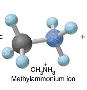
2 Perovskite Crystal with ABX 3 stoichiometry A X B I-V-O3, II-IV-O3 and III-III-O3 e.g KTaO3, SrTiO3 and GdFeO3 I-II-X3, e.g. CsSnI3, CH3NH3PbI3, 2
3 It is not only a matter of stoichiometry. A X B The Goldschmidt tolerance factor: R A RX t 2( R B RX ) t< 0.7 the perovskite falls apart t >1 towards 2D structures 3
4 Playing with Dimensionality CH 3 NH 3 PbI 3 (CH 3 NH 3 ) 2 PbI 4 (C 10 H 21 NH 3 ) 2 PbI 4 (CH 3 NH 3 ) 4 PbI 6 *H 2 O 4
5 Dielectric Confinement CH 3 NH 3 PbI 3 (CH 3 NH 3 ) 2 PbI 4 (C 10 H 21 NH 3 ) 2 PbI 4 (CH 3 NH 3 ) 4 PbI 6 *H 2 O Ishihara, J. Lum,
6 Organo-Metal Halide Crystalline Perovskite ABX 3 B = (CH 3 NH 3+ ) x X= I -, Cl -, Br - A= Pb 2+ 6


7 Organo-Metal Halide Crystalline Perovskite Filip et al, Nat Comm, 2014 Eric Hoke et al, Chem Sci,

8 Organo-Metal Halide Crystalline Perovskite 8


9 CH3NH3 + :Orientational disorder and Polarizability Hydrogen Bonds Dipole nearly free to move 9


10 Modular Structure 10

11 Prone to a variety of processing methods 11

12 Excitonic Solar Cells Type II Hetero-Junction
13 Voc (V) Intrinsic Loss in Excitonic Solar Cells 1.2 Voc = BG -0.2eV -0.4eV -0.6eV Si CIGS GaAs CdTe DSC MSSC OPV asi 0.6 ncsi CZTSS Bandgap (ev) 13


14 Hybrid Crystals in DSSC Devices CH 3 NH 3 PbI 3 perovskite as light antenna in the DSSC concept e- injection h u Hole transfer H. S. Kim et al. Sci Rep. 2: 591 (2012)


15 Hybrid Crystals in Hybrid Solar Cells Silver HTL Perovskite role: Absorber Electron-transporter FTO TiO2 Al2O3 Glass M.Lee et al. Science 338, 643 (2012)
16 Which is their strength? 16


17 17


18 Optoelectronic Devices Zhu et al, Nat Mat, 2015 Tan et al, Nat Nanotech,

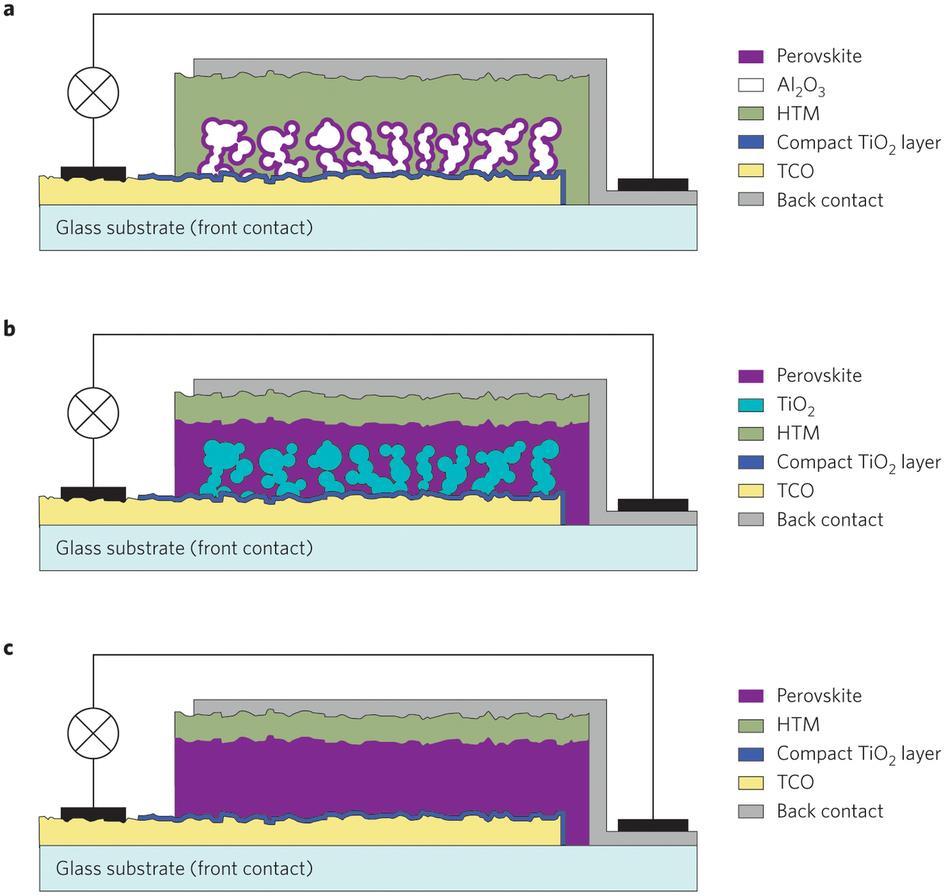
19 Designing the Device Architecture HTM TiO2/Al2O3 scaffold+ Perovskite HTM Perovkite capping layer HTM Perovkite capping layer J. Ball, EES, 2013 Nano-structured vs Thin Film 19
20 Designing the Device Architecture Light Absorption Charge Generation Photo-carriers Transport
21 Designing the Device Architecture Light Absorption Charge Generation Photo-carriers Transport
22 Silicon Light Absorption GaAs Dyes/conjugated polymers In direct band-gap Phonon assisted um range sun light penetration depth thick solar cells no light emission direct band-gap excitonic effects at absorption edge good light penetration depth localized states excitonic effects large absorption cross-section/ efficient carrier recombination
23 Silicon Light Absorption GaAs Dyes/conjugated polymers In direct bandgapphonon assisted um range visible light penetration dept thick solar cells no light emission direct band-gap excitonic effects at absorption edge good light penetration depth localized states excitonic effects large absorption cross-section/ efficient carrier recombination
24 Optical Density (a.u.) Silicon Light Absorption Hybrid Perovskites Dyes/conjugated polymers K 290K In direct bandgapphonon assisted um range visible light penetration dept thick solar cells no light emission Energy (ev) direct band-gap excitonic effects at absorption edge good light penetration depth localized states excitonic effects large absorption cross-section/ efficient carrier recombination


25 Exciton..is a quasi-particle that represents a collective excited state of an ensable of atoms or molecules. It is represented by a wavepacket for which we can define mass and speed which transports Energy 25

26 How many kind of excitons?? Wannier-Mott Frenkel Binding energy Delocalization Oscillator strength Triplet Singlet Lifetime 26
27 Frenkel Exciton Solids made by weakly interacting units (e.g organic crystals, inter-molecular coupling weaker than the intra-molecular ones). General case of a Molecular Excitation (DSSC) The wavefunction squared amplitude is the probability of finding the excited state in the lattice. G. Lanzani, The Photophysics behind Photovoltaics and Photonics Wiley-VCH E u g De e 27
28 Wannier-Mott Solids with tightly bounded atoms Low Screening Coulomb attraction does not allow the generation of FREE e-h pairs Hydrogenoid system. Center of Mass/Exciton radius (LARGER than E the lattice constant) k e k h R X r h r e O 2 2 Eb K X EK X, n Eg 2 n m m e G. Lanzani, The Photophysics behind Photovoltaics and Photonics Wiley-VCH h E 1 K E g
29 Why do we need to know the details? Energy spent in the exciton dissociation
30 Why do we need to know the details? Energy spent in the exciton dissociation Absoprtion cross section enhancement X 1 ( a B 3 )
31 Why do we need to know the details? Energy spent in the exciton dissociation Absoprtion cross section enhancement Elliott s Theory (1963)
32 Exciton Vs Free Charges at the Thermodynamic Equilibrium Total excitation density Excitons n n FC n exc PV RT n n FC exc Free charges 2 k ( h Law of mass action T B ) 3/ 2 2 e Eb k T Saha-Langmiur equation B D Innocenzo et al, Nat Comm. 5, 3586, 2014 x n FC n 32
33 Exciton Binding Energy Exciton Reduced mass E B Dielectric constant 4 2 e e 2 a 2 B 2 e a B 2 e memh m m h Bohr Radius e The golden rule: the Bohr orbital frequency (E b /h) must be compared with the optical phonon frequency
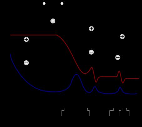
34 Dielectric constant (ε): A measure of a substance s ability to insulate charges from each other.
35 Screening in solids: basic concept E 0 METAL DIELECTRIC E=0 E d E d = E 0 ε
36 Screening mechanisms Electronic Polarizability (Electron Cloud Distortion) s -1 Dipole Re Orientation (Langevin Mechanism) s -1 Ions Displacement s -1 (Optical Phonons)
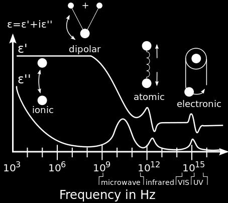
37 Screening mechanisms
38 Dielectric constant of GaAs. Why it is so easy e 0 2 e e 0 (T) = *T LO = 36meV TO = 38meV
39 Dielectric constants of CH3NH3PbI3, real and imaginary parts
40 Dielectric constants of CH3NH3PbI3, real and imaginary parts 1KHz
41 (I) Direct Measurement of Exciton Binding Energy in CH 3 NH 3 PbI 3 Exciton Binding Energy hd D u k 1 u exp( k E B b T ) E b (upper limit)= 50meV Limitations: It is assumed that exciton-phonon interaction induces only exciton dissociation though in a limited range it assumes the exciton binding energy constant in T D Innocenzo et al, Nat Comm. 5, 3586,
42 (I) Direct Measurement of Exciton Binding Energy in CH 3 NH 3 PbI 3 D 1 T 2 1 T T 1 1 k k T 0 T 1 k T e T E B k B T 42


43 (II) Direct Measurement of Exciton Binding Energy in CH 3 NH 3 PbI 3 Numerical modelling of band-edge absorption by using Elliot s theory of Wannier excitons E b = 25meV Note: This simple formalism does not consider the frequency dependance of the exciton-phonon interaction Saba et al, Nat Comm. 5, 5049,
44 (III) Direct Measurement of Exciton Binding Energy in CH 3 NH 3 PbI 3 E( B) Eg ( N 1/ 2) ( eb ) m* E n E g R n At 4K m*= 0.1m ; E b = 16meV Miyata et al, Nature Physics 11, (2015) e 9 44
 m* E n E g R n At 161K E b 10 mev Miyata et al, Nature Physics 11, 582 587 (2015) e > 9")
45 (III) Direct Measurement of Exciton Binding Energy in CH 3 NH 3 PbI 3 E( B) Eg ( N 1/ 2) ( eb ) m* E n E g R n At 161K E b 10 mev Miyata et al, Nature Physics 11, (2015) e > 9 45
46 Raman I (norm.units) Organic-Inorganic Interplay: Raman Spectroscopy as a probe 1.0 Meso Flat Raman shift (cm-1) Grancini G et al, JPC Letters, 5, 3836, 2014
47 Light Absorption Charge Generation Photo-carriers Transport
48 Exciton Vs Free Charges Total excitation density at the Thermodynamic Equilibrium n n FC n Free charges exc Excitons n n FC exc 2 k ( h 2 B T ) 3/ 2 e Eb k T B x n FC n Saha-Langmuir equation 48

49 Are there excitons around? MAPbI 3 Room Temperature, in the typical PV regime ph <10 16 cm -3 : free carriers only THz conductivity spectra are Drude-like in accordance with the presence of free charge carriers. Wehrefenning et al, Adv Mater, 26, 1584, 2014, Milot et al, Adv Funct Mater, 2015 DOI: /adfm , PL dynamics are dictated by bimolecular recombination processes. Yamada, Y J. Am. Chem. Soc. 2014, 136, Stranks, Phys. Rev. Appl. 2014, fs-ta spectra show band filling effect and Varnshi shift. Kamat et al, Nature Photonics, 2014; Grancini&Kandada et al, Nature Photonics 2015 The deal for PV is: we exploit the presence of the exciton transition for light harvesting without paying in charge dissociation
50 x (n FC /n TOT ) Are there excitons around? MAPbI 3 Low Temperature, Exciton population is detectable K 170K 70K mev Excitation Density (cm -3 ) THz spectra probe localization effects as a consequence of exciton formation below 80K. Milot et al, Adv Funct Mater, 2015 DOI: /adfm , fs-ta spectra show a modulation of the photo-bleach as a result of exciton-exciton interaction. Grancini&Kandada et al, Nature Photonics 2015 WARNING: The Exciton binding energy increases (the dielectric constant decreases) when cooling down! Miyata et al, Nature Physics 11, (2015)
51 Local order/ microstructure MAPbI 3 D Innocenzo et al, Nat Comm. 5, 3586, 2014 Grancini&Kandada et al, Nature Photonics 2015
52 Designing the Device Architecture Light Absorption Charge Generation Photo-carriers Transport
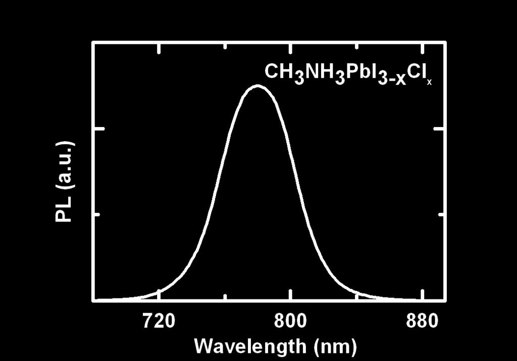
53 O.D. PL (norm.) Photo-carriers Diffusion Length CH 3 NH 3 PbI 3-x Cl x /PMMA Wavelength (nm)
54 Electron-Hole Diffusion Lengths By Photoluminescence Quenching Glass Silica Selective Quencher Diffusion constant Natural decay rate (no quencher) 54
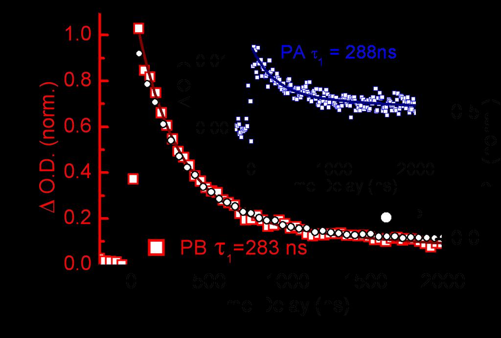

55 Electron-Hole Diffusion Lengths By Photoluminescence Quenching DT (n e +n h ) CB VB Science, 342,341,
56 PL (norm.) PL (norm.) Electron-Hole Diffusion Lengths By Photoluminescence Quenching CH 3 NH 3 PbI 3 PMMA Spiro-OMeTAD PCBM CH 3 NH 3 PbI 3-x Cl x PMMA Spiro-OMeTAD PCBM Time after excitation (ns) Time after excitation (ns) Perovskite Species D (cm 2 s -1 ) L D (nm) CH 3 NH 3 PbI 3-x Cl x Electrons ± ± 210 Holes ± ± 250 CH 3 NH 3 PbI 3 Electrons ± ± 29 Science, 342,341, 2013 Holes ± ± 22 56
57 Time-resolved Photoluminescence Stranks et al Yamada, Y J. Am. Chem. Soc. 2014, 136, Stranks, Phys. Rev. Appl. 2014, Saba, M.; Nat. Commun. 2014, 5 No D Innocenzo, J. Am. Chem. Soc. 2014, 136 (51), pp Deschler, J. Phys. Chem. Lett. 2014, 5, Deschler, et al
58 Time-resolved Photoluminescence D Innocenzo et al. JACS, 2014, 136 (51), pp
, pp 17730 1773 R i rad n ( E ( E G G ) ) E CBB E G ph ( e ) ( e ) v ( e ) 1 e 1 ph (e ) k B ( e ) de T de Filippetti, et al. J.Phys.Chem, 2014, 59 doi:10.")
59 Spectral position (nm) Time-resolved Photoluminescence Band Edge Position cwpl Peak Position Avarage crystallite size (nm) D Innocenzo et al. JACS, 2014, 136 (51), pp R i rad n ( E ( E G G ) ) E CBB E G ph ( e ) ( e ) v ( e ) 1 e 1 ph (e ) k B ( e ) de T de Filippetti, et al. J.Phys.Chem, 2014, 59 doi: /jp507430x

 Hall-effect Simultaneously get free-carrier density Like THz, only band mobility obtained μ ~ 66 cm 2 /Vs Q. Dong et al., Science (2015) C.")
60 Measuring Charge-Transport in Perovskites Terahertz/Microwave Spectroscopy Simple sample preparation Only informative on short length-scale μ ~ 10 cm 2 /Vs Time-of-flight Relevant over longer length-scale Time-scales difficult to measure in thin-film μ ~ 25 cm 2 /Vs C. Wehrenfennig et al., Adv. Mat. (2013) Space-charge limited current Relevant to optoelectronic devices Needs highly-selective non-limiting contacts μ ~ cm 2 /Vs Q. Dong et al., Science (2015) Hall-effect Simultaneously get free-carrier density Like THz, only band mobility obtained μ ~ 66 cm 2 /Vs Q. Dong et al., Science (2015) C. Stoumpos et al., Inorg. Chem. (2013)
61 Take-home Message The room temperature structure of MAPbX3 is a fluctuating structure where titling and distortion of the octahedral networks and rotations and polarizability of the molecular dipole can strongly affect the optoelectronic properties of the semiconductor.
62 Open Questions Which is the secret of the low recombination rate Elucidation of the photo-carriers cooling Role of phonons Nature of carriers, localization vs delocalization Carriers transport mechanism Vs Structural Properties
63 Technology
64 Technology
65 Technology Zhang et al, Mater. Horiz., 2015, 2,

66 Perovskite PV at IIT p I n Spiro MeOTAD MAPbI 3 TiO x /PCBM


67 Perovskite PV at IIT Technology Development Fotovoltaico leggero e flessibile, a basso costo di produzione e energetico 17.6 % p I n Aumento efficienza fotovoltaico tradizionale Processi a bassa temperatura < 120 C Celle «TANDEM» 67
68 Further Developments Interface Engineering Stability Toxicity..
Opto-electronic Characterization of Perovskite Thin Films & Solar Cells
 Opto-electronic Characterization of Perovskite Thin Films & Solar Cells Arman Mahboubi Soufiani Supervisors: Prof. Martin Green Prof. Gavin Conibeer Dr. Anita Ho-Baillie Dr. Murad Tayebjee 22 nd June 2017
The Current Status of Perovskite Solar Cell Research at UCLA
 The Current Status of Perovskite Solar Cell Research at UCLA Lijian Zuo, Sanghoon Bae, Lei Meng, Yaowen Li, and Yang Yang* Department of Materials Science and Engineering University of California, Los
Supporting Information for. Modulating the Electron - Hole Interaction in a Hybrid Lead Halide. Perovskite with an Electric Field
 Supporting Information for Modulating the Electron - Hole Interaction in a Hybrid Lead Halide Perovskite with an Electric Field Tomas Leijtens 1,2, Ajay Ram Srimath Kandada 1, Giles E. Eperon 2, Giulia
Intensity / a.u. 2 theta / deg. MAPbI 3. 1:1 MaPbI 3-x. Cl x 3:1. Supplementary figures
 Intensity / a.u. Supplementary figures 110 MAPbI 3 1:1 MaPbI 3-x Cl x 3:1 220 330 0 10 15 20 25 30 35 40 45 2 theta / deg Supplementary Fig. 1 X-ray Diffraction (XRD) patterns of MAPbI3 and MAPbI 3-x Cl
(002)(110) (004)(220) (222) (112) (211) (202) (200) * * 2θ (degree)
(110) (004)(220) (222) (112) (211) (202) (200) * * 2θ (degree)") Supplementary Figures. (002)(110) Tetragonal I4/mcm Intensity (a.u) (004)(220) 10 (112) (211) (202) 20 Supplementary Figure 1. X-ray diffraction (XRD) pattern of the sample. The XRD characterization indicates
Supplementary Figures. (002)(110) Tetragonal I4/mcm Intensity (a.u) (004)(220) 10 (112) (211) (202) 20 Supplementary Figure 1. X-ray diffraction (XRD) pattern of the sample. The XRD characterization indicates
Physics of Organic Semiconductor Devices: Materials, Fundamentals, Technologies and Applications
 Physics of Organic Semiconductor Devices: Materials, Fundamentals, Technologies and Applications Dr. Alex Zakhidov Assistant Professor, Physics Department Core faculty at Materials Science, Engineering
Recent Developments in Perovskite Materials for Solar Cell Applications. Yu Sheng Min, Researcher of ITRI/MCL
 Recent Developments in Perovskite Materials for Solar Cell Applications Yu Sheng Min, Researcher of ITRI/MCL 2017.10.19 Outline Introduction of perovskite materials Major problems of perovskite solar cells
CHARGE CARRIERS PHOTOGENERATION. Maddalena Binda Organic Electronics: principles, devices and applications Milano, November 23-27th, 2015
 CHARGE CARRIERS PHOTOGENERATION Maddalena Binda Organic Electronics: principles, devices and applications Milano, November 23-27th, 2015 Charge carriers photogeneration: what does it mean? Light stimulus
Supplementary Figure 1 Two-dimensional map of the spin-orbit coupling correction to the scalar-relativistic DFT/LDA band gap. The calculations were
 Supplementary Figure 1 Two-dimensional map of the spin-orbit coupling correction to the scalar-relativistic DFT/LDA band gap. The calculations were performed for the Platonic model of PbI 3 -based perovskites
Charge-Carrier Dynamics in Organic-Inorganic Metal Halide Perovskites
 ANNUAL REVIEWS Further Click here to view this article's online features: Download figures as PPT slides Navigate linked references Download citations Explore related articles Search keywords Annu. Rev.
Photovoltaics. Lecture 7 Organic Thin Film Solar Cells Photonics - Spring 2017 dr inż. Aleksander Urbaniak
 Photovoltaics Lecture 7 Organic Thin Film Solar Cells Photonics - Spring 2017 dr inż. Aleksander Urbaniak Barcelona, Spain Perpignan train station, France source: pinterest Why organic solar cells? 1.
Exciton spectroscopy
 Lehrstuhl Werkstoffe der Elektrotechnik Exciton spectroscopy in wide bandgap semiconductors Lehrstuhl Werkstoffe der Elektrotechnik (WW6), Universität Erlangen-Nürnberg, Martensstr. 7, 91058 Erlangen Vortrag
Supporting Information. Femtosecond Time-Resolved Transient Absorption. Passivation Effect of PbI 2
 Supporting Information Femtosecond Time-Resolved Transient Absorption Spectroscopy of CH 3 NH 3 PbI 3 -Perovskite Films: Evidence for Passivation Effect of PbI 2 Lili Wang a, Christopher McCleese a, Anton
Probing Femtosecond Lattice Displacement upon Photo-carrier generation
 Probing Femtosecond Lattice Displacement upon Photo-carrier generation in Lead Halide Perovskite Giovanni Batignani 1±, Giuseppe Fumero 1,2±, Ajay Ram Srimath Kandada 3±, Giulio Cerullo 4, Marina Gandini
Basic Limitations to Third generation PV performance
 Basic Limitations to Third generation PV performance Pabitra K. Nayak Weizmann Institute of Science, Rehovot, Israel THANKS to my COLLEAGUES Lee Barnea and David Cahen. Weizmann Institute of Science Juan
Solar Cell Materials and Device Characterization
 Solar Cell Materials and Device Characterization April 3, 2012 The University of Toledo, Department of Physics and Astronomy SSARE, PVIC Principles and Varieties of Solar Energy (PHYS 4400) and Fundamentals
Chemistry Instrumental Analysis Lecture 8. Chem 4631
 Chemistry 4631 Instrumental Analysis Lecture 8 UV to IR Components of Optical Basic components of spectroscopic instruments: stable source of radiant energy transparent container to hold sample device
Novel Inorganic-Organic Perovskites for Solution Processed Photovoltaics. PIs: Mike McGehee and Hema Karunadasa
 Novel Inorganic-Organic Perovskites for Solution Processed Photovoltaics PIs: Mike McGehee and Hema Karunadasa 1 Perovskite Solar Cells are Soaring Jul 2013 Grätzel, EPFL 15% Nov 2014 KRICT 20.1%! Seok,
Mesoporous titanium dioxide electrolyte bulk heterojunction
 Mesoporous titanium dioxide electrolyte bulk heterojunction The term "bulk heterojunction" is used to describe a heterojunction composed of two different materials acting as electron- and a hole- transporters,
Role of coherence and delocalization in photo-induced electron transfer at organic interfaces
 Supplementary Information to Role of coherence and delocalization in photo-induced electron transfer at organic interfaces V. Abramavicius,, V. Pranckevičius, A. Melianas, O. Inganäs, V. Gulbinas, D. Abramavicius
Supplementary Figure 1 Transient absorption (TA) spectrum pumped at 400 nm in the FAPbI3 sample with different excitation intensities and initial
 spectrum pumped at 400 nm in the FAPbI3 sample with different excitation intensities and initial") Supplementary Figure 1 Transient absorption (TA) spectrum pumped at 400 nm in the FAPbI3 sample with different excitation intensities and initial carrier concentrations: (a) N0 = 4.84 10 18 cm -3 ; (c)
Supplementary Figure 1 Transient absorption (TA) spectrum pumped at 400 nm in the FAPbI3 sample with different excitation intensities and initial carrier concentrations: (a) N0 = 4.84 10 18 cm -3 ; (c)
University of Louisville - Department of Chemistry, Louisville, KY; 2. University of Louisville Conn Center for renewable energy, Louisville, KY; 3
 Ultrafast transient absorption spectroscopy investigations of charge carrier dynamics of methyl ammonium lead bromide (CH 3 NH 3 PbBr 3 ) perovskite nanostructures Hamzeh Telfah 1 ; Abdelqader Jamhawi
Quantum Dots for Advanced Research and Devices
 Quantum Dots for Advanced Research and Devices spectral region from 450 to 630 nm Zero-D Perovskite Emit light at 520 nm ABOUT QUANTUM SOLUTIONS QUANTUM SOLUTIONS company is an expert in the synthesis
Optical Properties of Solid from DFT
 Optical Properties of Solid from DFT 1 Prof.P. Ravindran, Department of Physics, Central University of Tamil Nadu, India & Center for Materials Science and Nanotechnology, University of Oslo, Norway http://folk.uio.no/ravi/cmt15
Supplementary Figures
 Supplementary Figures Supplementary Figure. X-ray diffraction pattern of CH 3 NH 3 PbI 3 film. Strong reflections of the () family of planes is characteristics of the preferred orientation of the perovskite
Luminescence basics. Slide # 1
 Luminescence basics Types of luminescence Cathodoluminescence: Luminescence due to recombination of EHPs created by energetic electrons. Example: CL mapping system Photoluminescence: Luminescence due to
Luminescence Process
 Luminescence Process The absorption and the emission are related to each other and they are described by two terms which are complex conjugate of each other in the interaction Hamiltonian (H er ). In an
Optical Properties of Semiconductors. Prof.P. Ravindran, Department of Physics, Central University of Tamil Nadu, India
 Optical Properties of Semiconductors 1 Prof.P. Ravindran, Department of Physics, Central University of Tamil Nadu, India http://folk.uio.no/ravi/semi2013 Light Matter Interaction Response to external electric
Lecture 8 Interband Transitions. Excitons
 Lecture 8 Interband Transitions Excitons Read: FS 4 Purdue University Spring 2016 Prof. Yong P. Chen (yongchen@purdue.edu) Lecture 8 (2/4/2016) Slide 1 Textbook 1: M. Fox Optical Properties of Solids (2
Time resolved optical spectroscopy methods for organic photovoltaics. Enrico Da Como. Department of Physics, University of Bath
 Time resolved optical spectroscopy methods for organic photovoltaics Enrico Da Como Department of Physics, University of Bath Outline Introduction Why do we need time resolved spectroscopy in OPV? Short
Lecture 6 Optical Characterization of Inorganic Semiconductors Dr Tim Veal, Stephenson Institute for Renewable Energy and Department of Physics,
 Lecture 6 Optical Characterization of Inorganic Semiconductors Dr Tim Veal, Stephenson Institute for Renewable Energy and Department of Physics, University of Liverpool Lecture Outline Lecture 6: Optical
Yixin Zhao and Kai Zhu*
 Supporting Information CH 3 NH 3 Cl-Assisted One-Step Solution Growth of CH 3 NH 3 PbI 3 : Structure, Charge- Carrier Dynamics, and Photovoltaic Properties of Perovskite Solar Cells Yixin Zhao and Kai
Review of Optical Properties of Materials
 Review of Optical Properties of Materials Review of optics Absorption in semiconductors: qualitative discussion Derivation of Optical Absorption Coefficient in Direct Semiconductors Photons When dealing
Temperature Dependent Optical Band Gap Measurements of III-V films by Low Temperature Photoluminescence Spectroscopy
 Temperature Dependent Optical Band Gap Measurements of III-V films by Low Temperature Photoluminescence Spectroscopy Linda M. Casson, Francis Ndi and Eric Teboul HORIBA Scientific, 3880 Park Avenue, Edison,
Lecture contents. Burstein shift Excitons Interband transitions in quantum wells Quantum confined Stark effect. NNSE 618 Lecture #15
 1 Lecture contents Burstein shift Excitons Interband transitions in quantum wells Quantum confined Stark effect Absorption edges in semiconductors Offset corresponds to bandgap Abs. coefficient is orders
Supporting Information. Polaron Self-localization in White-light. Emitting Hybrid Perovskites
 Electronic Supplementary Material (ESI) for Journal of Materials Chemistry C. This journal is The Royal Society of Chemistry 2017 Supporting Information Polaron Self-localization in White-light Emitting
ET3034TUx Utilization of band gap energy
 ET3034TUx - 3.3.1 - Utilization of band gap energy In the last two weeks we have discussed the working principle of a solar cell and the external parameters that define the performance of a solar cell.
Winter College on Optics and Energy February Photophysics for photovoltaics. G. Lanzani CNST of Milano Italy
 13-4 Winter College on Optics and Energy 8-19 February 010 Photophysics for photovoltaics G. Lanzani CNST of IIT@POLIMI Milano Italy Winter College on Optics and Energy Guglielmo Lanzani CNST of IIT@POLIMI,
Iodine chemistry determines the defect tolerance of leadhalide
 Electronic Supplementary Material (ESI) for Energy & Environmental Science. This journal is The Royal Society of Chemistry 2018 Iodine chemistry determines the defect tolerance of leadhalide perovskites
Supplementary Figure 1 XRD pattern of a defective TiO 2 thin film deposited on an FTO/glass substrate, along with an XRD pattern of bare FTO/glass
 Supplementary Figure 1 XRD pattern of a defective TiO 2 thin film deposited on an FTO/glass substrate, along with an XRD pattern of bare FTO/glass and a reference pattern of anatase TiO 2 (JSPDS No.: 21-1272).
Charge separation in molecular donor acceptor heterojunctions
 Institute of Physics 13 July 2009 Charge separation in molecular donor acceptor heterojunctions Jenny Nelson, James Kirkpatrick, Jarvist Frost, Panagiotis Keivanidis, Clare Dyer-Smith, Jessica Benson-Smith
Highly efficient hybrid perovskite solar cells by interface engineering
 Highly efficient hybrid perovskite solar cells by interface engineering Maria Antonietta Loi Photophysics & OptoElectronics Zernike Institute for Advanced Materials University of Groningen The Netherlands
Optical Science of Nano-graphene (graphene oxide and graphene quantum dot) Introduction of optical properties of nano-carbon materials
 Introduction of optical properties of nano-carbon materials") Optical Science of Nano-graphene (graphene oxide and graphene quantum dot) J Kazunari Matsuda Institute of Advanced Energy, Kyoto University Introduction of optical properties of nano-carbon materials
Optical Science of Nano-graphene (graphene oxide and graphene quantum dot) J Kazunari Matsuda Institute of Advanced Energy, Kyoto University Introduction of optical properties of nano-carbon materials
Supporting information. Supramolecular Halogen Bond Passivation of Organometal-Halide Perovskite Solar Cells
 Supporting information Supramolecular Halogen Bond Passivation of Organometal-Halide Perovskite Solar Cells Antonio Abate, a Michael Saliba, a Derek J. Hollman, a Samuel D. Stranks, a K. Wojciechowski,
High efficiency silicon and perovskite-silicon solar cells for electricity generation
 High efficiency silicon and perovskite-silicon solar cells for electricity generation Ali Dabirian Email: dabirian@ipm.ir 1 From Solar Energy to Electricity 2 Global accumulative PV installed In Iran it
2.626 Fundamentals of Photovoltaics
 MIT OpenCourseWare http://ocw.mit.edu 2.626 Fundamentals of Photovoltaics Fall 2008 For information about citing these materials or our Terms of Use, visit: http://ocw.mit.edu/terms. Charge Separation:
Research Article Plasmonic Structure Enhanced Exciton Generation at the Interface between the Perovskite Absorber and Copper Nanoparticles
 e Scientific World Journal, Article ID 128414, 6 pages http://dx.doi.org/1.1155/214/128414 Research Article Plasmonic Structure Enhanced Exciton Generation at the Interface between the Perovskite Absorber
Three-Dimensional Silicon-Germanium Nanostructures for Light Emitters and On-Chip Optical. Interconnects
 Three-Dimensional Silicon-Germanium Nanostructures for Light Emitters and On-Chip Optical eptember 2011 Interconnects Leonid Tsybeskov Department of Electrical and Computer Engineering New Jersey Institute
PHOTOVOLTAICS Fundamentals
 PHOTOVOLTAICS Fundamentals PV FUNDAMENTALS Semiconductor basics pn junction Solar cell operation Design of silicon solar cell SEMICONDUCTOR BASICS Allowed energy bands Valence and conduction band Fermi
SUPPLEMENTARY INFORMATION
 Supplementary Information Efficient inorganic-organic hybrid heterojunction solar cells containing perovskite compound and polymeric hole conductors Jin Hyuck Heo, Sang Hyuk Im, Jun Hong Noh, Tarak N.
Photo-Reactivity. Jerusalem, Israel. Israel
 Electronic Supplementary Material (ESI) for Physical Chemistry Chemical Physics. This journal is the Owner Societies 2018 CsPbBr 3 and CH 3 NH 3 PbBr 3 Promote Visible-light Photo-Reactivity Shankar Harisingh
Generalized picture 1
 one electron energy contact contact The Photovoltaic (PV) effect: Generalized picture 1 Absorber e - High energy state Metastable high and low energy states Absorber transfers charges into high and low
Photocarrier Recombination and Injection Dynamics in Long-Term Stable Lead-Free CH 3 NH 3 SnI 3 Perovskite Thin Films and Solar Cells
 Supporting Information Photocarrier Recombination and Injection Dynamics in Long-Term Stable Lead-Free CH 3 NH 3 SnI 3 Perovskite Thin Films and Solar Cells Taketo Handa, + Takumi Yamada, + Hirofumi Kubota,
Fermi polaron-polaritons in MoSe 2
 Fermi polaron-polaritons in MoSe 2 Meinrad Sidler, Patrick Back, Ovidiu Cotlet, Ajit Srivastava, Thomas Fink, Martin Kroner, Eugene Demler, Atac Imamoglu Quantum impurity problem Nonperturbative interaction
Communicating Two States in Perovskite Revealed by Time-Resolved Photoluminescence Spectroscopy
 Communicating Two States in Perovskite Revealed by Time-Resolved Photoluminescence Spectroscopy Yanwen Chen #1, Tianmeng Wang #1, Zhipeng Li 1,2, Huanbin Li 1,3, Tao Ye 3, Christian Wetzel 4, Hanying Li
Semiconductor quantum dots
 Semiconductor quantum dots Quantum dots are spherical nanocrystals of semiconducting materials constituted from a few hundreds to a few thousands atoms, characterized by the quantum confinement of the
Supplementary Figure S1. Verifying the CH 3 NH 3 PbI 3-x Cl x sensitized TiO 2 coating UV-vis spectrum of the solution obtained by dissolving the
 Supplementary Figure S1. Verifying the CH 3 NH 3 PbI 3-x Cl x sensitized TiO 2 coating UV-vis spectrum of the solution obtained by dissolving the spiro-ometad from a perovskite-filled mesoporous TiO 2
3.1 Introduction to Semiconductors. Y. Baghzouz ECE Department UNLV
 3.1 Introduction to Semiconductors Y. Baghzouz ECE Department UNLV Introduction In this lecture, we will cover the basic aspects of semiconductor materials, and the physical mechanisms which are at the
Supplementary Information: Hot Carrier Cooling and Photoinduced. Refractive Index Changes in Organic-Inorganic Lead Halide
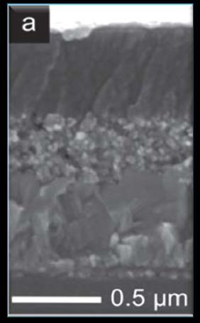
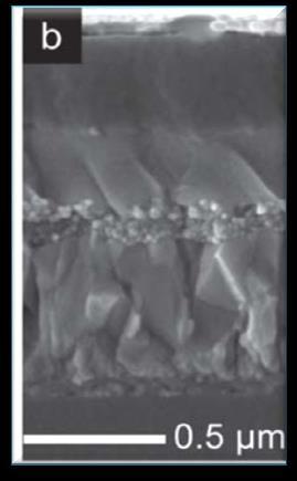
 Supplementary Information: Hot Carrier Cooling and Photoinduced Refractive Index Changes in Organic-Inorganic Lead Halide Perovskites. a b Supplementary Figure 1: Scanning electron microscopy of films
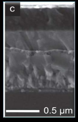
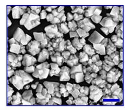
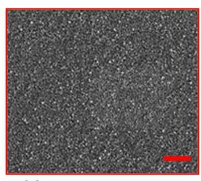
i) impact of interchain interactions
 impact of interchain interactions") i) impact of interchain interactions multiple experimental observations: in dilute solutions or inert matrices: the photoluminescence quantum yield of a given conjugated polymers can be very large: up
i) impact of interchain interactions multiple experimental observations: in dilute solutions or inert matrices: the photoluminescence quantum yield of a given conjugated polymers can be very large: up
PH575 Spring Lecture #20 Semiconductors: optical properties: Kittel Ch. 8 pp ; Ch 15 pp
 PH575 Spring 2014 Lecture #20 Semiconductors: optical properties: Kittel Ch. 8 pp. 187-191; Ch 15 pp. 435-444 Figure VI-1-1: Different types of optical absorption phenomena; (1) transitions of highlying
Organic Solar Cells. All Organic solar cell. Dye-sensitized solar cell. Dye. τ inj. τ c. τ r surface states D*/D + V o I 3 D/D.
 The 4th U.S.-Korea NanoForum April 26-27, 2007, Honolulu, USA Improvement of Device Efficiency in Conjugated Polymer/Fullerene NanoComposite Solar Cells School of Semiconductor & Chemical Engineering *
EE495/695 Introduction to Semiconductors I. Y. Baghzouz ECE Department UNLV
 EE495/695 Introduction to Semiconductors I Y. Baghzouz ECE Department UNLV Introduction Solar cells have always been aligned closely with other electronic devices. We will cover the basic aspects of semiconductor
Charge carriers photogeneration. Maddalena Binda Organic Electronics: principles, devices and applications Milano, November 26-29th, 2013
 Charge carriers photogeneration Maddalena Binda Organic Electronics: principles, devices and applications Milano, November 26-29th, 2013 Charge carriers photogeneration: what does it mean? Light stimulus
Supplementary Figure 1. Film thickness measurement. (a) AFM images of the perovskite
 AFM images of the perovskite") Supplementary Figure 1. Film thickness measurement. (a) AFM images of the perovskite film with a straight edge which was created by scratching with a tweezer. (b) Profile along the line highlighted in
Supplementary Figure 1. Film thickness measurement. (a) AFM images of the perovskite film with a straight edge which was created by scratching with a tweezer. (b) Profile along the line highlighted in
Latest achievements in the field of dye sensitized and perovskite solar cells Anders Hagfeldt Laboratory of Photomolecular Sciences (LSPM)
") 15 e Congrès photovoltaïque national, Lausanne, March 23, 2017 Latest achievements in the field of dye sensitized and perovskite solar cells Anders Hagfeldt Laboratory of Photomolecular Sciences (LSPM)
15 e Congrès photovoltaïque national, Lausanne, March 23, 2017 Latest achievements in the field of dye sensitized and perovskite solar cells Anders Hagfeldt Laboratory of Photomolecular Sciences (LSPM)
Optical Investigation of the Localization Effect in the Quantum Well Structures
 Department of Physics Shahrood University of Technology Optical Investigation of the Localization Effect in the Quantum Well Structures Hamid Haratizadeh hamid.haratizadeh@gmail.com IPM, SCHOOL OF PHYSICS,
Basic cell design. Si cell
 Basic cell design Si cell 1 Concepts needed to describe photovoltaic device 1. energy bands in semiconductors: from bonds to bands 2. free carriers: holes and electrons, doping 3. electron and hole current:
interband transitions in semiconductors M. Fox, Optical Properties of Solids, Oxford Master Series in Condensed Matter Physics
 interband transitions in semiconductors M. Fox, Optical Properties of Solids, Oxford Master Series in Condensed Matter Physics interband transitions in quantum wells Atomic wavefunction of carriers in
(Co-PIs-Mark Brongersma, Yi Cui, Shanhui Fan) Stanford University. GCEP Research Symposium 2013 Stanford, CA October 9, 2013
 Stanford University. GCEP Research Symposium 2013 Stanford, CA October 9, 2013") High-efficiency thin film nano-structured multi-junction solar James S. cells Harris (PI) (Co-PIs-Mark Brongersma, Yi Cui, Shanhui Fan) Stanford University GCEP Research Symposium 2013 Stanford, CA October
High-efficiency thin film nano-structured multi-junction solar James S. cells Harris (PI) (Co-PIs-Mark Brongersma, Yi Cui, Shanhui Fan) Stanford University GCEP Research Symposium 2013 Stanford, CA October
Multiple Exciton Generation in Quantum Dots. James Rogers Materials 265 Professor Ram Seshadri
 Multiple Exciton Generation in Quantum Dots James Rogers Materials 265 Professor Ram Seshadri Exciton Generation Single Exciton Generation in Bulk Semiconductors Multiple Exciton Generation in Bulk Semiconductors
Organic solar cells. State of the art and outlooks. Gilles Horowitz LPICM, UMR7647 CNRS - Ecole Polytechnique
 Organic solar cells. State of the art and outlooks Gilles Horowitz LPICM, UMR7647 CNRS - Ecole Polytechnique Solar energy Solar energy on earth: 75,000 tep/year 6000 times the world consumption in 2007
Supplementary Materials
 Supplementary Materials Sample characterization The presence of Si-QDs is established by Transmission Electron Microscopy (TEM), by which the average QD diameter of d QD 2.2 ± 0.5 nm has been determined
Triplet state diffusion in organometallic and organic semiconductors
 Triplet state diffusion in organometallic and organic semiconductors Prof. Anna Köhler Experimental Physik II University of Bayreuth Germany From materials properties To device applications Organic semiconductors
Nanotechnology and Solar Energy. Solar Electricity Photovoltaics. Fuel from the Sun Photosynthesis Biofuels Split Water Fuel Cells
 Nanotechnology and Solar Energy Solar Electricity Photovoltaics Fuel from the Sun Photosynthesis Biofuels Split Water Fuel Cells Solar cell A photon from the Sun generates an electron-hole pair in a semiconductor.
Direct Observation of Long Electron-Hole Diffusion
 Direct Observation of Long Electron-Hole Diffusion Distance in CH3NH3PbI3 Perovskite Thin Film Yu Li 1,, Weibo Yan 2,, Yunlong Li 2, Shufeng Wang 1, *, Wei Wang 1, Zuqiang Bian 2, *, Lixin Xiao 1, and
OPTICAL PROPERTIES of Nanomaterials
 OPTICAL PROPERTIES of Nanomaterials Advanced Reading Optical Properties and Spectroscopy of Nanomaterials Jin Zhong Zhang World Scientific, Singapore, 2009. Optical Properties Many of the optical properties
Nanoscience galore: hybrid and nanoscale photonics
 Nanoscience galore: hybrid and nanoscale photonics Pavlos Lagoudakis SOLAB, 11 June 2013 Hybrid nanophotonics Nanostructures: light harvesting and light emitting devices 2 Hybrid nanophotonics Nanostructures:
Accelerated Carrier Relaxation through Reduced Coulomb Screening in Two-Dimensional Halide Perovskite Nanoplatelets
 Supporting Information Accelerated Carrier Relaxation through Reduced Coulomb Screening in Two-Dimensional Halide Perovskite Nanoplatelets Verena A. Hintermayr 1,2, Lakshminarayana Polavarapu 1,2, Alexander
Electrons are shared in covalent bonds between atoms of Si. A bound electron has the lowest energy state.
 Photovoltaics Basic Steps the generation of light-generated carriers; the collection of the light-generated carriers to generate a current; the generation of a large voltage across the solar cell; and
smal band gap Saturday, April 9, 2011
 small band gap upper (conduction) band empty small gap valence band filled 2s 2p 2s 2p hybrid (s+p)band 2p no gap 2s (depend on the crystallographic orientation) extrinsic semiconductor semi-metal electron
Introduction. Fang-Chung Chen Department of Photonics and Display Institute National Chiao Tung University. Organic light-emitting diodes
 rganic light-emitting diodes Introduction Fang-Chung Chen Department of Photonics and Display Institute National Chiao Tung University rganic light-emitting diodes --The emerging technology LED Displays
Direct and Indirect Semiconductor
 Direct and Indirect Semiconductor Allowed values of energy can be plotted vs. the propagation constant, k. Since the periodicity of most lattices is different in various direction, the E-k diagram must
Electronic and Optoelectronic Properties of Semiconductor Structures
 Electronic and Optoelectronic Properties of Semiconductor Structures Jasprit Singh University of Michigan, Ann Arbor CAMBRIDGE UNIVERSITY PRESS CONTENTS PREFACE INTRODUCTION xiii xiv 1.1 SURVEY OF ADVANCES
Organo-metal halide perovskite-based solar cells with CuSCN as inorganic hole selective contact
 Electronic Supplementary Material (ESI) for Journal of Materials Chemistry A. This journal is The Royal Society of Chemistry 214 Organo-metal halide perovskite-based solar cells with CuSCN as inorganic
Organic Electronic Devices
 Organic Electronic Devices Week 5: Organic Light-Emitting Devices and Emerging Technologies Lecture 5.5: Course Review and Summary Bryan W. Boudouris Chemical Engineering Purdue University 1 Understanding
Lecture 15: Optoelectronic devices: Introduction
 Lecture 15: Optoelectronic devices: Introduction Contents 1 Optical absorption 1 1.1 Absorption coefficient....................... 2 2 Optical recombination 5 3 Recombination and carrier lifetime 6 3.1
Towards a deeper understanding of polymer solar cells
 Towards a deeper understanding of polymer solar cells Jan Anton Koster Valentin Mihailetchi Prof. Paul Blom Molecular Electronics Zernike Institute for Advanced Materials and DPI University of Groningen
Strong light matter coupling in two-dimensional atomic crystals
 SUPPLEMENTARY INFORMATION DOI: 10.1038/NPHOTON.2014.304 Strong light matter coupling in two-dimensional atomic crystals Xiaoze Liu 1, 2, Tal Galfsky 1, 2, Zheng Sun 1, 2, Fengnian Xia 3, Erh-chen Lin 4,
Ultra-stable 2D/3D hybrid perovskite photovoltaic module
 Ultra-stable 2D/3D hybrid perovskite photovoltaic module Giulia Grancini 1, Cristina Roldán-Carmona 1, Iwan Zimmermann 1, David Martineau 2, Stéphanie Narbey 2, Frédéric Oswald 2, Mohammad Khaja Nazeeruddin
Vibronic Coupling in Quantum Wires: Applications to Polydiacetylene
 Vibronic Coupling in Quantum Wires: Applications to Polydiacetylene An Exhaustively Researched Report by Will Bassett and Cole Johnson Overall Goal In order to elucidate the absorbance spectra of different
Flexible Organic Photovoltaics Employ laser produced metal nanoparticles into the absorption layer 1. An Introduction
 Flexible Organic Photovoltaics Employ laser produced metal nanoparticles into the absorption layer 1. An Introduction Among the renewable energy sources that are called to satisfy the continuously increased
Electronic and optical properties of graphene- and graphane-like SiC layers
 Electronic and optical properties of graphene- and graphane-like SiC layers Paola Gori, ISM, CNR, Rome, Italy Olivia Pulci, Margherita Marsili, Università di Tor Vergata, Rome, Italy Friedhelm Bechstedt,
Supporting Information
 Electronic Supplementary Material (ESI) for Nanoscale. This journal is The Royal Society of Chemistry 2015 Supporting Information Single Layer Lead Iodide: Computational Exploration of Structural, Electronic
Center for Integrated Nanostructure Physics (CINAP)
") Center for Integrated Nanostructure Physics (CINAP) - Institute for Basic Science (IBS) was launched in 2012 by the Korean government to promote basic science in Korea - Our Center was established in 2012
Center for Integrated Nanostructure Physics (CINAP) - Institute for Basic Science (IBS) was launched in 2012 by the Korean government to promote basic science in Korea - Our Center was established in 2012
Polariton Condensation
 Polariton Condensation Marzena Szymanska University of Warwick Windsor 2010 Collaborators Theory J. Keeling P. B. Littlewood F. M. Marchetti Funding from Macroscopic Quantum Coherence Macroscopic Quantum
Capturing Energy from the Sun. Solar Cells Solar Thermal Solar Fuels Bioenergy
 Capturing Energy from the Sun Solar Cells Solar Thermal Solar Fuels Bioenergy Installed PV Cost Breakdown a Globally, module prices are between $0.60-0.90/W depending on tariffs In the US, non-module costs
Observation of charged excitons in hole-doped carbon nanotubes using photoluminescence and absorption spectroscopy
 Observation of charged excitons in hole-doped carbon nanotubes using photoluminescence and absorption spectroscopy Ryusuke Matsunaga 1, Kazunari Matsuda 1, and Yoshihiko Kanemitsu 1,2 1 Institute for Chemical
OPTICAL PROPERTIES AND SPECTROSCOPY OF NANOAAATERIALS. Jin Zhong Zhang. World Scientific TECHNISCHE INFORMATIONSBIBLIOTHEK
 OPTICAL PROPERTIES AND SPECTROSCOPY OF NANOAAATERIALS Jin Zhong Zhang University of California, Santa Cruz, USA TECHNISCHE INFORMATIONSBIBLIOTHEK Y World Scientific NEW JERSEY. t'on.don SINGAPORE «'BEIJING
Fluorescence Spectroscopy
 Fluorescence Spectroscopy Frequency and time dependent emission Emission and Excitation fluorescence spectra Stokes Shift: influence of molecular vibrations and solvent Time resolved fluorescence measurements