Research Article Plasmonic Structure Enhanced Exciton Generation at the Interface between the Perovskite Absorber and Copper Nanoparticles
|
|
|
- Nigel Jennings
- 6 years ago
- Views:
Transcription
1 e Scientific World Journal, Article ID , 6 pages Research Article Plasmonic Structure Enhanced Exciton Generation at the Interface between the Perovskite Absorber and Copper Nanoparticles Sheng Hsiung Chang, 1 Kuen-Feng Lin, 2 Chien-Hung Chiang, 1 Sheng-Hui Chen, 2 and Chun-Guey Wu 1 1 Research Center for New Generation Photovoltaics, National Central University, No. 3 Jhongda Road, Jhongli, Taoyuan County 321, Taiwan 2 Department of Optics and Photonics, National Central University, No. 3 Jhongda Road, Jhongli, Taoyuan County 321, Taiwan Correspondence should be addressed to Sheng Hsiung Chang; shchang@ncu.edu.tw, Sheng-Hui Chen; ericchen@dop.ncu.edu.tw, and Chun-Guey Wu; t612@cc.ncu.edu.tw Received 3 June 214; Revised 5 August 214; Accepted 19 August 214; Published 11 September 214 Academic Editor: Rui C. Marques Copyright 214 Sheng Hsiung Chang et al. This is an open access article distributed under the Creative Commons Attribution License, which permits unrestricted use, distribution, and reproduction in any medium, provided the original work is properly cited. The refractive index and extinction coefficient of a triiodide perovskite absorber (TPA) were obtained by fitting the transmittance spectra of TPA/PEDOT:PSS/ITO/glass using the transfer matrix method. Cu nanoplasmonic structures were designed to enhance the exciton generation in the TPA and to simultaneously reduce the film thickness of the TPA. Excitons were effectively generated at the interface between TPA and Cu nanoparticles, as observed through the 3D finite-difference time-domain method. The exciton distribution is advantageous for the exciton dissociation and carrier transport. 1. Introduction In recent years, mixed halide (CH 3 NH 3 PbI 3 x Cl x ) and triiodide (CH 3 NH 3 PbI 3 ) perovskite absorber (PA) based photovoltaics have been intensively investigated because a power conversion efficiency (PCE) of 15% can be achieved by solution processes under low temperatures [1, 2]. There are several factors that can explain the high PCE. The bandgap of PA is about 4 ev [3], which can absorb half of the sun light. The exciton diffusion length of PA is longer than 1 micrometer[4]; therefore the bilayered structure based photovoltaics are workable [1 4]. The exciton binding energy of PA is about 5 mev [5], which results in good exciton dissociation at the interface between the PA and PCBM (Spiro-OMeTAD) [4]. The sharp optical absorption edge of PA corresponds to the small Urbach energy ( 15 mev), which results in a high fill factor [6]. The thickness of PA has to be 4 nm in order to efficiently absorb the incident sun light. However, a thicker PA is disadvantageous for exciton dissociation and carrier transport, limiting the photovoltaic performances in terms of short-circuit current density and fill factor. A PCE as high as 2% can be expected by improving the fill factor [7]. The above-mentioned drawbacks can be improved by using nanoplasmonic structures [8, 9]. Two degenerate transverse plasmon modes are supported by twodimensional ordered Cu nanoplasmonic structure embedded in P3HT:PCBM blended film, which has been designed to enhance the absorption of P3HT:PCBM based inverted photovoltaics by 22% in the visible range [9]. In this work, the Cu nanoplasmonic structures were used to enhance exciton generation in the triiodide perovskite absorber (TPA) while simultaneously reducing the film thickness of TPA. The transfer matrix method (TMM) was used to calculate the transmittance, reflectance, and absorptance. The 3D finitedifference time-domain (FDTD) method was used to observe the plasmon-mediated exciton generation.
2 2 The Scientific World Journal Transmittance (%) Refractive index Extinction coefficient TPA/PEDOT:PSS/ITO/glass Fitting curve Refractive index Extinction coefficient Figure 1: Transmittance spectra of TPA/PEDOT:PSS/ITO/glass under normal incidence. Refractive index and extinction coefficient of TPA film. 2. Optical Constants of Triiodide Perovskite Absorber TPAwasspin-coatedontopofthePEDOT:PSS/ITO/glassby a sequential deposition method [1]. Figure 1 presents the transmittance spectrum of the TPA/PEDOT:PSS/ITO/glass. The transmittance spectrum was measured by a high accuracy spectrometer (Hitachi U-41). The film thickness for each layer was measured by an α-step device (Veeco Dektak 15).ThethicknessesoftheTPA,PEDOT:PSS,andITO werefoundtobe4nm,2nm,and25nm,respectively. The refractive indices and extinction coefficients of the PEDOT:PSS thin film and the ITO film were taken from [9]. A Lorentz model was used to describe the dielectric constant of TPA, which can be written as follows: 14 s n ω L,n ε TPA (ω) =ε b + n=1ωl,n 2 ω2 jg n ω, (1) where ε b (=1.5) is the background dielectric constant, n is the nth Lorentz pole, s n is the strength, ω L is the oscillation frequency, and G is the decay rate. Fourteen Lorentz oscillators were used in the fitting process. The transmittance spectrum of the TPA/PEDOT:PSS/ITO/glass was fitted using TMM. The fourteen oscillating wavelengths λ L werefixed and are listed in Table 1. λ L = 2πc/ω L,wherec is light speed in vacuum. The oscillation strengths and decay rates were scanned in the fitting process. An error function (EF) is defined to evaluate the accuracy between fitting and experimental curves. Consider 75 EF = T fit (λ) T exp (λ), (2) 351 T λ=4 exp where T fit (red line) is the transmittance of the fitting curve and T exp (black line) is the measured transmittance of the Table 1: Fitted parameters of the Lorentz model for TPA film. Oscillation wavelength (nm) Strength Decay rate ( 1 14 /s) λ L,1 = 38 s 1 =.2 G 1 =1 λ L,2 = 43 s 2 =.15 G 2 =8 λ L,3 = 47 s 3 =.1 G 3 =6 λ L,4 = 5 s 4 =.4 G 4 =4 λ L,5 = 52 s 5 =.35 G 5 = 3.5 λ L,6 = 54 s 6 =.32 G 6 = 3.5 λ L,7 = 57 s 7 =.3 G 7 =4 λ L,8 = 6 s 8 =.2 G 8 =4 λ L,9 = 63 s 9 =.2 G 9 =4 λ L,1 = 67 s 1 =.2 G 1 = 3.5 λ L,11 = 71 s 11 =.15 G 11 =3 λ L,12 = 72 s 12 =.8 G 12 =3 λ L,13 = 73 s 13 =.9 G 13 =2 λ L,14 = 745 s 14 =.1 G 14 = 1.5 TPA/PEDOT:PSS/ITO/glass. The value of the error function is equal to.25. The refractive index n and extinction coefficient k of the TPA film can be obtained by n+ ik = (ε TPA ) 1/2.TheopticalconstantsofTPAareplotted infigure 1. The fitted parameters are listed in Table Plasmonic Structure Enhanced Exciton Generation Figure 2 presents the absorptance spectra of the TPA/ITO/glass, which was calculated using TMM. The absorptance of the TPA increases with an increase in thickness
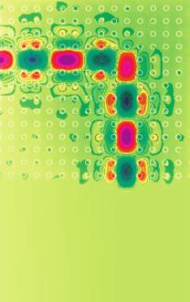
3 The Scientific World Journal Absorptance (%) TPA/ITO/glass Thickness of TPA film 4 nm 3 nm 2 nm Figure 2: Absorptance spectra of TPA/ITO/glass for different TPA thicknesses. Triiodide perovskite absorber y t rod D Cu t TPA x Unit cell ITO (25 nm) P Glass substrate Figure 3: Side view of TPA/ITO/glass with the Cu nanoplasmonic structure. Top view of the Cu nanoplasmonic structure embedded in the TPA thin film. from 2 nm to 4 nm. In the wavelength range of 8 nm to 9 nm, the incident near-infrared light is absorbed by the ITO film due to the free carrier absorption. In order to reduce the thickness, a Cu nanoplasmonic structure was embedded in the TPA in order to enhance the absorptance in the effective absorption range (35 nm to 76 nm). Figure 3 presents the Cu nanoplasmonic structure embedded in the TPA thin film. In this study, the period P wasfixedat 1 nm. The gap size is defined by the difference between the period and the diameter of Cu nanoparticles. The dipole-coupling model (DCM) [1] was adopted to calculate the effective dielectric constant of Cu nanoplasmonic structure embedded in the TPA film. These nanoplasmonic structures embedded can be treated as an effective medium. The physical concept of DCM is described in [9]. The Lorentz-Drude model was applied to Cu to calculate the refractive index and absorption coefficient [11]. Figure4 presents the absorptance spectra of the TPA with and without the Cu nanoplasmonic structures. There wasanincreaseintheabsorptanceofthetpawithcu nanoplasmonic structures when the gap was changed from 5 nm to 3 nm. Compared with the red dashed line (TPA thickness = 2 nm) in Figure 4, the absorptance indicated by the black line is larger because the transverse plasmonic (TP) mode enhances the absorption (exciton generation) of the TPA. Compared with the black dashed line (TPA thickness = 4 nm) in Figure 4, the absorptance indicated by the black line is smaller. The absorptance spectra of a thicker TPA film with and without Cu nanoplasmonic structures are presented in Figure5. Compared with
4 4 The Scientific World Journal Absorptance (%) 6 Absorptance (%) TPA thickness: TPA thickness = 2 nm 4 nm Gap: 2 nm 5 nm 4 nm 3 nm Figure 4: The red (black) dashed line indicates the absorptance of the TPA/ITO/glass when the TPA thickness is equal to 2 nm (4 nm). The blue, red, and black lines are the absorptance of the TPA/ITO/glass with the Cu nanoplasmonic structure when the long axis of the Cu nanoparticles is 1 nm. TPA thickness: TPA thickness = 3 nm 4 nm Gap: 3 nm 5 nm 4 nm 3 nm Figure 5: The red (black) dashed line indicated the absorptance of the TPA/ITO/glass when the TPA thickness is equal to 3 nm (4 nm). The blue, red, and black lines show the absorptance of the TPA/ITO/glass with the Cu nanoplasmonic structure when the long axis of the Cu nanoparticles is 15 nm. the black dashed line (TPA thickness = 4 nm) in Figure 5, the absorptance indicated by the black line is higher due to the TP mode enhanced absorption even though the TPA thickness (=3 nm) is thinner. The Cu nanoplasmonic structure enhanced the absorptance of TPA in the effective absorption range (35 nm 76 nm) by 1.7% while reducing the TPA thickness from 4 nm to 3 nm. 4. Exciton Distribution The 3D FDTD method was used to calculate the electric and magnetic field distributions of the Cu nanoplasmonic structures embedded in the TPA film. 2-cell perfectly matching layers were imposed at upper and lower boundaries to absorb the outgoing electromagnetic waves without producing significant reflections back into the simulation domain. The simulation of two-dimensional ordered Cu nanoparticle arrays was performed using periodic boundary conditions. The cell size and the time step used in discretization of the space domain and time domain were 1 nm 1nm 1nm and s, respectively. A planewave with an x-directed electric field was launched from the glass substrate along the positive z-direction. Figure 6 presents the field distributions of the x-y plane at the resonant wavelength of TP mode. The strengths of electric field and magnetic field both increased when the gap was changed from 5 nm to 3 nm. The incident light is trapped and redistributed in space to effectively generate excitons at the interface between the TPA and Cu nanoparticles. Conceptually, the excitons can be dissociated at the interface between TPA and Cu nanoparticles because the HOMO level ( 5.4 ev) [3] of the TPA is lower than the Fermi level of Cu ( 4.94 ev) [12]. Therefore, the localized field distribution benefits the exciton dissociation. Figure 7 presents the electric field distributions of Cu nanoplasmonic structures embedded in the TPA film on the x-z plane. The electric fields (excitons) are localized (generated) around the lower surface of Cu nanoparticles. Therefore,theexcitonsaredissociatedmostlyfromthelower surface of the Cu nanoparticles. After exciton dissociation, the holes (electrons) can propagate along the Cu (TPA) to the anode (cathode) electrode. In such cases, carrier recombination can be reduced. 5. Conclusions In conclusion, we have assessed the optical effects of Cu nanoplasmonic structure embedded in triiodide perovskite absorber (TPA). The refractive index and absorption coefficientoftpawereobtainedbyfittingthetransmittancespectrum of TPA/PEDOT:PSS/ITO/glass using transfer matrix method. Cu nanoplasmonic structures could reduce the TPAthicknessfrom4nmto3nmwhilekeepingthe absorption strength. The 3D finite-difference time-domain method was used to observe the distribution of the electric field (generated excitons). The electric field is redistributed at the interface between the TPA and Cu nanoparticles, which benefits the exciton dissociation and carrier transport.


 field distributions of the")
")

5 The Scientific World Journal 5 16 Gap = 5 nm Gap = 4 nm Gap = 3 nm (c) Gap = 5 nm Gap = 4 nm Gap = 3 nm H 8 H 8 H (d) (e) (f) Figure 6:,, and (c) ((d), (e), and (f)) are the electric (magnetic) field distributions of the x-y plane for different gap sizes. 4 Gap = 5 nm 4 Gap = 4 nm 4 Gap = 3 nm 3 TPA 3 3 z (nm) 2 Cu ITO (c) Figure 7:,, and (c) are the electric field distributions of the x-z plane for different gap sizes.
6 6 The Scientific World Journal Conflict of Interests The authors declare that there is no conflict of interests regarding the publication of this paper. Acknowledgment This work was supported by the National Science Council under Grant NSC M-8-2-MY3. References [1] J. Burschka, N. Pellet, S.-J. Moon et al., Sequential deposition as a route to high-performance perovskite-sensitized solar cells, Nature,vol.499,no.7458,pp ,213. [2]D.LiuandT.L.Kelly, Perovskitesolarcellswithaplanar heterojunction structure prepared using room-temperature solution processing techniques, Nature Photonics, vol. 8, pp , 214. [3]G.Xing,N.Mathews,S.Sunetal., Long-rangebalanced electron- and hole-transport lengths in organic-inorganic CH 3 NH 3 PbI 3, Science,vol.342,pp ,213. [4] S.D.Stranks,G.E.Eperon,G.Grancinietal., Electron-hole diffusion lengths exceeding 1 micrometer in an organometal trihalide perovskite absorber, Science, vol.342,pp , 213. [5] V. D'Innocenzo, G. Grancini, J. P. Marcelo et al., Excitons versus free charges in organo-lead tri-halide perovskites, Nature Communications,vol.5,article3586,214. [6] S. de Wolf, J. Holovsky, S.-J. Moon et al., Organometallic halide perovskites: sharp optical absorption edge and its relation to photovoltaic performance, TheJournalofPhysicalChemistry Letters,vol.5,no.6,pp ,214. [7] N.-G. Park, Organometal perovskite light absorbers toward a 2% efficiency low-cost solid-state mesoscopic solar cell, The Physical Chemistry Letters, vol.4,no.15,pp , 213. [8] N. F. Fahim, B. Jia, Z. Shi, and M. Gu, Simultaneous broadband light trapping and fill factor enhancement in crystalline silicon solar cells induced by Ag nanoparticles and nanoshells, Optics Express,vol.2,no.19,pp.A694 A75,212. [9] S.H.Chang, ModelinganddesignofAg,Au,andCunanoplasmonic structures for enhancing the absorption of P3HT:PCBMbased photovoltaics, IEEE Photonics Journal, vol.5,no.3, Article ID 4859, 213. [1] S. H. Chang, B.-Y. Lin, T.-Y. Cheng, and J.-K. Wang, Unraveling electromagnetic resonance of two-dimensional ordered nanoparticle arrays with a dipole-coupling model, Physica Status Solidi: Rapid Research Letters,vol.4,no.1,pp , 21. [11] A. D. Rakić, A. B. Djurišić, J. M. Elazar, and M. L. Majewski, Optical properties of metallic films for vertical-cavity optoelectronic devices, Applied Optics, vol.37,no.22,pp , [12] P. O. Gartland, S. Berge, and B. J. Slagsvold, Photoelectric work function of a copper single crystal for the (1), (11), (111), and (112) faces, Physical Review Letters,vol.28,no.12,pp , 1972.


7 The Scientific World Journal Gravity Photonics Advances in Condensed Matter Physics Soft Matter Aerodynamics Fluids Submit your manuscripts at International International Optics Statistical Mechanics Thermodynamics Computational Methods in Physics Solid State Physics Astrophysics Physics Research International Advances in High Energy Physics International Superconductivity Atomic and Molecular Physics Biophysics Advances in Astronomy
Research Article Visible Light Communication System Using Silicon Photocell for Energy Gathering and Data Receiving
 Hindawi International Optics Volume 2017, Article ID 6207123, 5 pages https://doi.org/10.1155/2017/6207123 Research Article Visible Light Communication System Using Silicon Photocell for Energy Gathering
Propagation of Surface Plasmon Polariton in the Single Interface of Gallium Lanthanum Sulfide and Silver
 PHOTONIC SENSORS / Vol., No., : 58 6 Propagation of Surface Plasmon Polariton in the Single Interface of Gallium Lanthanum Sulfide and Silver Rakibul Hasan SAGOR, Md. Ghulam SABER *, and Md. Ruhul AMIN
Flexible Organic Photovoltaics Employ laser produced metal nanoparticles into the absorption layer 1. An Introduction
 Flexible Organic Photovoltaics Employ laser produced metal nanoparticles into the absorption layer 1. An Introduction Among the renewable energy sources that are called to satisfy the continuously increased
(002)(110) (004)(220) (222) (112) (211) (202) (200) * * 2θ (degree)
(110) (004)(220) (222) (112) (211) (202) (200) * * 2θ (degree)") Supplementary Figures. (002)(110) Tetragonal I4/mcm Intensity (a.u) (004)(220) 10 (112) (211) (202) 20 Supplementary Figure 1. X-ray diffraction (XRD) pattern of the sample. The XRD characterization indicates
Supplementary Figures. (002)(110) Tetragonal I4/mcm Intensity (a.u) (004)(220) 10 (112) (211) (202) 20 Supplementary Figure 1. X-ray diffraction (XRD) pattern of the sample. The XRD characterization indicates
Research Article Si Substrate-Based Metamaterials for Ultrabroadband Perfect Absorption in Visible Regime
 Nanomaterials, Article ID 893202, 5 pages http://dx.doi.org/0.55/204/893202 Research Article Si Substrate-Based Metamaterials for Ultrabroadband Perfect in Visible Regime Qi Han, Lei Jin, Yongqi Fu, and
Supplementary Figure S1. Hole collection layer photovoltaic performance in perovskite solar cells. Current voltage curves measured under AM1.
 Supplementary Figure S1. Hole collection layer photovoltaic performance in perovskite solar cells. Current voltage curves measured under AM1.5 simulated sun light at 100mWcm -2 equivalent irradiance for
The Current Status of Perovskite Solar Cell Research at UCLA
 The Current Status of Perovskite Solar Cell Research at UCLA Lijian Zuo, Sanghoon Bae, Lei Meng, Yaowen Li, and Yang Yang* Department of Materials Science and Engineering University of California, Los
Organic Electronic Devices
 Organic Electronic Devices Week 4: Organic Photovoltaic Devices Lecture 4.1: Overview of Organic Photovoltaic Devices Bryan W. Boudouris Chemical Engineering Purdue University 1 Lecture Overview and Learning
Supporting Information
 Electronic Supplementary Material (ESI) for Journal of Materials Chemistry A. This journal is The Royal Society of Chemistry 2018 Supporting Information A minimal non-radiative recombination loss for efficient
Optical Properties of Solid from DFT
 Optical Properties of Solid from DFT 1 Prof.P. Ravindran, Department of Physics, Central University of Tamil Nadu, India & Center for Materials Science and Nanotechnology, University of Oslo, Norway http://folk.uio.no/ravi/cmt15
Opto-electronic Characterization of Perovskite Thin Films & Solar Cells
 Opto-electronic Characterization of Perovskite Thin Films & Solar Cells Arman Mahboubi Soufiani Supervisors: Prof. Martin Green Prof. Gavin Conibeer Dr. Anita Ho-Baillie Dr. Murad Tayebjee 22 nd June 2017
Supplementary Figure 1 XRD pattern of a defective TiO 2 thin film deposited on an FTO/glass substrate, along with an XRD pattern of bare FTO/glass
 Supplementary Figure 1 XRD pattern of a defective TiO 2 thin film deposited on an FTO/glass substrate, along with an XRD pattern of bare FTO/glass and a reference pattern of anatase TiO 2 (JSPDS No.: 21-1272).
Plasmonics. The long wavelength of light ( μm) creates a problem for extending optoelectronics into the nanometer regime.
 creates a problem for extending optoelectronics into the nanometer regime.") Plasmonics The long wavelength of light ( μm) creates a problem for extending optoelectronics into the nanometer regime. A possible way out is the conversion of light into plasmons. They have much shorter
Plasmonics The long wavelength of light ( μm) creates a problem for extending optoelectronics into the nanometer regime. A possible way out is the conversion of light into plasmons. They have much shorter
Research Article Trapped-Mode Resonance Regime of Thin Microwave Electromagnetic Arrays with Two Concentric Rings in Unit Cell
 Microwave Science and Technology Volume 2, Article ID 3688, 6 pages doi:.55/2/3688 Research Article Trapped-Mode Resonance Regime of Thin Microwave Electromagnetic Arrays with Two Concentric Rings in Unit
Photovoltaics. Lecture 7 Organic Thin Film Solar Cells Photonics - Spring 2017 dr inż. Aleksander Urbaniak
 Photovoltaics Lecture 7 Organic Thin Film Solar Cells Photonics - Spring 2017 dr inż. Aleksander Urbaniak Barcelona, Spain Perpignan train station, France source: pinterest Why organic solar cells? 1.
Optical Properties of Semiconductors. Prof.P. Ravindran, Department of Physics, Central University of Tamil Nadu, India
 Optical Properties of Semiconductors 1 Prof.P. Ravindran, Department of Physics, Central University of Tamil Nadu, India http://folk.uio.no/ravi/semi2013 Light Matter Interaction Response to external electric
Review of Optical Properties of Materials
 Review of Optical Properties of Materials Review of optics Absorption in semiconductors: qualitative discussion Derivation of Optical Absorption Coefficient in Direct Semiconductors Photons When dealing
Light Concentration in Polymer Bulk Heterojunction Solar Cells with Plasmonic Nanoparticles
 Light Concentration in Polymer Bulk Heterojunction Solar Cells with Plasmonic Nanoparticles Jinfeng Zhu* a, Baoqing Zeng* a, Richard S. Kim b, Zhe Wu a, a School of Physical Electronics, University of
Supporting Information. Fully Solution-Processed Semitransparent Organic Solar Cells with a Silver Nanowire Cathode and a Conducting Polymer Anode
 Supporting Information Fully Solution-Processed Semitransparent Organic Solar Cells with a Silver Nanowire Cathode and a Conducting Polymer Anode Jong Hyuk Yim, Sung-yoon Joe, Christina Pang, Kyung Moon
Plasmonic Photovoltaics Harry A. Atwater California Institute of Technology
 Plasmonic Photovoltaics Harry A. Atwater California Institute of Technology Surface plasmon polaritons and localized surface plasmons Plasmon propagation and absorption at metal-semiconductor interfaces
Quantum Dots for Advanced Research and Devices
 Quantum Dots for Advanced Research and Devices spectral region from 450 to 630 nm Zero-D Perovskite Emit light at 520 nm ABOUT QUANTUM SOLUTIONS QUANTUM SOLUTIONS company is an expert in the synthesis
Supporting Information
 Supporting Information Modulation of PEDOT:PSS ph for Efficient Inverted Perovskite Solar Cells with Reduced Potential Loss and Enhanced Stability Qin Wang 1,2, Chu-Chen Chueh 1, Morteza Eslamian 2 * and
Ankara, Turkey Published online: 20 Sep 2013.
 This article was downloaded by: [Bilkent University] On: 26 December 2013, At: 12:33 Publisher: Taylor & Francis Informa Ltd Registered in England and Wales Registered Number: 1072954 Registered office:
Numerical model of planar heterojunction organic solar cells
 Article Materials Science July 2011 Vol.56 No.19: 2050 2054 doi: 10.1007/s11434-011-4376-4 SPECIAL TOPICS: Numerical model of planar heterojunction organic solar cells MA ChaoZhu 1 PENG YingQuan 12* WANG
Intensity / a.u. 2 theta / deg. MAPbI 3. 1:1 MaPbI 3-x. Cl x 3:1. Supplementary figures
 Intensity / a.u. Supplementary figures 110 MAPbI 3 1:1 MaPbI 3-x Cl x 3:1 220 330 0 10 15 20 25 30 35 40 45 2 theta / deg Supplementary Fig. 1 X-ray Diffraction (XRD) patterns of MAPbI3 and MAPbI 3-x Cl
Research Article Trial Application of Pulse-Field Magnetization to Magnetically Levitated Conveyor System
 Advances in Condensed Matter Physics Volume 2, Article ID 5657, pages doi:1.1155/2/5657 Research Article Trial Application of Pulse-Field Magnetization to Magnetically Levitated Conveyor System Yoshihito
Optical Characterization of CdTe Films for Solar Cell Applications
 Karachi University Journal of Science, 2011, 39, 1-5 1 Optical Characterization of CdTe Films for Solar Cell Applications Saeed Salem Babkair *, Najat Mohammad Al-Twarqi and Azhar Ahmad Ansari Department
Towards a deeper understanding of polymer solar cells
 Towards a deeper understanding of polymer solar cells Jan Anton Koster Valentin Mihailetchi Prof. Paul Blom Molecular Electronics Zernike Institute for Advanced Materials and DPI University of Groningen
OPTICAL Optical properties of multilayer systems by computer modeling
 Workshop on "Physics for Renewable Energy" October 17-29, 2005 301/1679-15 "Optical Properties of Multilayer Systems by Computer Modeling" E. Centurioni CNR/IMM AREA Science Park - Bologna Italy OPTICAL
Supplementary Figure 1
 Supplementary Figure 1 XRD patterns and TEM image of the SrNbO 3 film grown on LaAlO 3(001) substrate. The film was deposited under oxygen partial pressure of 5 10-6 Torr. (a) θ-2θ scan, where * indicates
FINITE-DIFFERENCE FREQUENCY-DOMAIN ANALYSIS OF NOVEL PHOTONIC
 FINITE-DIFFERENCE FREQUENCY-DOMAIN ANALYSIS OF NOVEL PHOTONIC WAVEGUIDES Chin-ping Yu (1) and Hung-chun Chang (2) (1) Graduate Institute of Electro-Optical Engineering, National Taiwan University, Taipei,
Supporting Information
 Supporting Information Spatially-resolved imaging on photocarrier generations and band alignments at perovskite/pbi2 hetero-interfaces of perovskite solar cells by light-modulated scanning tunneling microscopy
Supplementary Figure 1 Two-dimensional map of the spin-orbit coupling correction to the scalar-relativistic DFT/LDA band gap. The calculations were
 Supplementary Figure 1 Two-dimensional map of the spin-orbit coupling correction to the scalar-relativistic DFT/LDA band gap. The calculations were performed for the Platonic model of PbI 3 -based perovskites
Plasmonic fractals: ultrabroadband light trapping in thin film solar cells by a Sierpinski nanocarpet
 Plasmonic fractals: ultrabroadband light trapping in thin film solar cells by a Sierpinski nanocarpet Hanif Kazerooni 1, Amin Khavasi, 2,* 1. Chemical Engineering Faculty, Amirkabir University of Technology
The Dielectric Function of a Metal ( Jellium )
") The Dielectric Function of a Metal ( Jellium ) Total reflection Plasma frequency p (10 15 Hz range) Why are Metals Shiny? An electric field cannot exist inside a metal, because metal electrons follow the
The Dielectric Function of a Metal ( Jellium ) Total reflection Plasma frequency p (10 15 Hz range) Why are Metals Shiny? An electric field cannot exist inside a metal, because metal electrons follow the
Research Article Modeling and Simulation of a Resonant-Cavity-Enhanced InGaAs/GaAs Quantum Dot Photodetector
 Advances in Condensed Matter Physics Volume 215, Article ID 84751, 6 pages http://dx.doi.org/1.1155/215/84751 Research Article Modeling and Simulation of a Resonant-Cavity-Enhanced InGaAs/GaAs Quantum
(Co-PIs-Mark Brongersma, Yi Cui, Shanhui Fan) Stanford University. GCEP Research Symposium 2013 Stanford, CA October 9, 2013
 Stanford University. GCEP Research Symposium 2013 Stanford, CA October 9, 2013") High-efficiency thin film nano-structured multi-junction solar James S. cells Harris (PI) (Co-PIs-Mark Brongersma, Yi Cui, Shanhui Fan) Stanford University GCEP Research Symposium 2013 Stanford, CA October
High-efficiency thin film nano-structured multi-junction solar James S. cells Harris (PI) (Co-PIs-Mark Brongersma, Yi Cui, Shanhui Fan) Stanford University GCEP Research Symposium 2013 Stanford, CA October
Research Article Propagation Characteristics of Oblique Incident Terahertz Wave in Nonuniform Dusty Plasma
 Antennas and Propagation Volume 216, Article ID 945473, 6 pages http://dx.doi.org/1.1155/216/945473 Research Article Propagation Characteristics of Oblique Incident Terahert Wave in Nonuniform Dusty Plasma
Planar Organic Photovoltaic Device. Saiful I. Khondaker
 Planar Organic Photovoltaic Device Saiful I. Khondaker Nanoscience Technology Center and Department of Physics University of Central Florida http://www.physics.ucf.edu/~khondaker W Metal 1 L ch Metal 2
PH575 Spring Lecture #20 Semiconductors: optical properties: Kittel Ch. 8 pp ; Ch 15 pp
 PH575 Spring 2014 Lecture #20 Semiconductors: optical properties: Kittel Ch. 8 pp. 187-191; Ch 15 pp. 435-444 Figure VI-1-1: Different types of optical absorption phenomena; (1) transitions of highlying
Supplementary Figure 1 Scheme image of GIXD set-up. The scheme image of slot die
 Supplementary Figure 1 Scheme image of GIXD set-up. The scheme image of slot die printing system combined with grazing incidence X-ray diffraction (GIXD) set-up. 1 Supplementary Figure 2 2D GIXD images
Giant Gating Tunability of Optical Refractive Index in Transition Metal Dichalcogenide Monolayers
 Supporting Information Giant Gating Tunability of Optical Refractive Index in Transition Metal Dichalcogenide Monolayers Yiling Yu 1,2, Yifei Yu 1, Lujun Huang 1, Haowei Peng 3, Liwei Xiong 1,4 and Linyou
26% PK/silicon tandem solar cell with 1 cm 2 area H2020-LCE
 H2020-LCE-205- CHEOPS Production Technology to Achieve Low Cost and Highly Efficient Photovoltaic Perovskite Solar Cells Deliverable WP4 PK/c-Si SHJ tandem device development Author: Arnaud Walter (CSEM)
Optimizing the performance of metal-semiconductor-metal photodetectors by embedding nanoparticles in the absorption layer
 Journal of Electrical and Electronic Engineering 2015; 3(2-1): 78-82 Published online February 10, 2015 (http://www.sciencepublishinggroup.com/j/jeee) doi: 10.11648/j.jeee.s.2015030201.27 ISSN: 2329-1613
Highly efficient hybrid perovskite solar cells by interface engineering
 Highly efficient hybrid perovskite solar cells by interface engineering Maria Antonietta Loi Photophysics & OptoElectronics Zernike Institute for Advanced Materials University of Groningen The Netherlands
Origin and Whereabouts of Recombination in. Perovskite Solar Cells Supporting Information
 Origin and Whereabouts of Recombination in Perovskite Solar Cells Supporting Information Lidia Contreras-Bernal a, Manuel Salado a,b, Anna Todinova a, Laura Calio b, Shahzada Ahmad b, Jesús Idígoras a,
Supporting Information. The Potential of Multi-Junction Perovskite Solar Cells
 Supporting Information The Potential of Multi-Junction Perovskite Solar Cells Maximilian T. Hörantner 1,4 *, Tomas Leijtens 2, Mark E. Ziffer 3, Giles E. Eperon 3,5, M. Greyson Christoforo 4, Michael D.
Nanomaterials for Plasmonic Devices. Lih J. Chen
 Nanomaterials for Plasmonic Devices Lih J. Chen Department of Materials Science and Engineering, National Tsing Hua University, Hsinchu, Taiwan Papers on Plasmon: 75,000 (6/25/2018) Papers on Plasmonics:
Introduction to Organic Solar Cells
 Introduction to Organic Solar Cells Dr Chris Fell Solar Group Leader CSIRO Energy Technology, Newcastle, Australia Organic semiconductors Conductivity in polyacetylene 1970s Nobel Prize Alan J. Heeger
Research Article The Effect of Metal-Semiconductor Contact on the Transient Photovoltaic Characteristic of HgCdTe PV Detector
 The Scientific World Journal Volume 2013, Article ID 213091, 5 pages http://dx.doi.org/10.1155/2013/213091 Research Article The Effect of Metal-Semiconductor Contact on the Transient Photovoltaic Characteristic
Nanophotonics: solar and thermal applications
 Nanophotonics: solar and thermal applications Shanhui Fan Ginzton Laboratory and Department of Electrical Engineering Stanford University http://www.stanford.edu/~shanhui Nanophotonic Structures Photonic
Photocarrier Recombination and Injection Dynamics in Long-Term Stable Lead-Free CH 3 NH 3 SnI 3 Perovskite Thin Films and Solar Cells
 Supporting Information Photocarrier Recombination and Injection Dynamics in Long-Term Stable Lead-Free CH 3 NH 3 SnI 3 Perovskite Thin Films and Solar Cells Taketo Handa, + Takumi Yamada, + Hirofumi Kubota,
Breaking the Space Charge Limit in Organic Semiconductors by Novel Plasmon-Electrical Concept
 Breaking the Space Charge Limit in Organic Semiconductors by Novel Plasmon-Electrical Concept Wallace C.H. Choy, Wei E.I. Sha, Xuanhua Li, and Hugh L. Zhu Presenter: Wei E.I. Sha Email: wsha@eee.hku.hk
A Comprehensive Multiphysics Model for Organic Photovoltaics. A Comprehensive Multiphysics Model for Organic Photovoltaics
 A Comprehensive Multiphysics Model for Organic Photovoltaics Zi Shuai Wang, Wei E. I. Sha, and Wallace C. H. Choy Presenter: Wei E. I. Sha Email: wsha@eee.hku.hk Website: http://www.eee.hku.hk/~wsha Department
Supplementary Figure S1. Verifying the CH 3 NH 3 PbI 3-x Cl x sensitized TiO 2 coating UV-vis spectrum of the solution obtained by dissolving the
 Supplementary Figure S1. Verifying the CH 3 NH 3 PbI 3-x Cl x sensitized TiO 2 coating UV-vis spectrum of the solution obtained by dissolving the spiro-ometad from a perovskite-filled mesoporous TiO 2
Superconductivity Induced Transparency
 Superconductivity Induced Transparency Coskun Kocabas In this paper I will discuss the effect of the superconducting phase transition on the optical properties of the superconductors. Firstly I will give
Research on the Wide-angle and Broadband 2D Photonic Crystal Polarization Splitter
 Progress In Electromagnetics Research Symposium 2005, Hangzhou, China, August 22-26 551 Research on the Wide-angle and Broadband 2D Photonic Crystal Polarization Splitter Y. Y. Li, P. F. Gu, M. Y. Li,
2.626 Fundamentals of Photovoltaics
 MIT OpenCourseWare http://ocw.mit.edu 2.626 Fundamentals of Photovoltaics Fall 2008 For information about citing these materials or our Terms of Use, visit: http://ocw.mit.edu/terms. Charge Separation:
A One-Step Low Temperature Processing Route for Organolead Halide Perovskite Solar Cells
 Electronic Supplementary Information A One-Step Low Temperature Processing Route for Organolead Halide Perovskite Solar Cells Matthew J. Carnie, a Cecile Charbonneau, a Matthew L. Davies, b Joel Troughton,
PHOTOVOLTAICS Fundamentals
 PHOTOVOLTAICS Fundamentals PV FUNDAMENTALS Semiconductor basics pn junction Solar cell operation Design of silicon solar cell SEMICONDUCTOR BASICS Allowed energy bands Valence and conduction band Fermi
Simulated Study of Plasmonic Coupling in Noble Bimetallic Alloy Nanosphere Arrays
 CHAPTER 4 Simulated Study of Plasmonic Coupling in Noble Bimetallic Alloy Nanosphere Arrays 4.1 Introduction In Chapter 3, the noble bimetallic alloy nanosphere (BANS) of Ag 1-x Cu x at a particular composition
Metamaterials & Plasmonics
 Metamaterials & Plasmonics Exploring the Impact of Rotating Rectangular Plasmonic Nano-hole Arrays on the Transmission Spectra and its Application as a Plasmonic Sensor. Abstract Plasmonic nano-structures
Charge Extraction. Lecture 9 10/06/2011 MIT Fundamentals of Photovoltaics 2.626/2.627 Fall 2011 Prof. Tonio Buonassisi
 Charge Extraction Lecture 9 10/06/2011 MIT Fundamentals of Photovoltaics 2.626/2.627 Fall 2011 Prof. Tonio Buonassisi 2.626/2.627 Roadmap You Are Here 2.626/2.627: Fundamentals Every photovoltaic device
Organic Solar Cell: Optics in Smooth and Pyramidal Rough Surface
 IOSR Journal of Electrical and Electronics Engineering (IOSR-JEEE) e-issn: 2278-1676,p-ISSN: 2320-3331, Volume 10, Issue 4 Ver. III (July Aug. 2015), PP 67-72 www.iosrjournals.org Organic Solar Cell: Optics
All-Inorganic Perovskite Solar Cells
 Supporting Information for: All-Inorganic Perovskite Solar Cells Jia Liang, Caixing Wang, Yanrong Wang, Zhaoran Xu, Zhipeng Lu, Yue Ma, Hongfei Zhu, Yi Hu, Chengcan Xiao, Xu Yi, Guoyin Zhu, Hongling Lv,
Research Article P3HT:PCBM Incorporated with Silicon Nanoparticles as Photoactive Layer in Efficient Organic Photovoltaic Devices
 Nanomaterials Volume 2013, Article ID 354035, 4 pages http://dx.doi.org/10.1155/2013/354035 Research Article P3HT:PCBM Incorporated with Silicon Nanoparticles as Photoactive Layer in Efficient Organic
Supporting Information. Monolithic perovskite-homojunction silicon tandem solar cell with over 22% efficiency
 Electronic Supplementary Material (ESI) for Energy & Environmental Science. This journal is The Royal Society of Chemistry 2017 Electronic Supplementary Information (ESI) for Energy & Environmental Science
Hybrid Perovskite Solar Cells
 1 Hybrid Perovskite Solar Cells Annamaria Petrozza "ORGANIC ELECTRONICS : principles, devices and applications" Milan, Novembre 27 th, 2015 Perovskite Crystal with ABX 3 stoichiometry A X B I-V-O3, II-IV-O3
Organic solar cells with inverted layer sequence incorporating optical spacers - simulation and experiment.
 Organic solar cells with inverted layer sequence incorporating optical spacers - simulation and experiment. Birger Zimmermann a, Markus Glatthaar a, Michael Niggemann Author3 a,b, Moritz Kilian Riede b,
Research Article Wavelength Width Dependence of Cavity Temperature Distribution in Semiconductor Diode Laser
 ISRN Thermodynamics Volume 213, Article ID 42475, 6 pages http://dx.doi.org/1.1155/213/42475 Research Article Wavelength Width Dependence of Cavity Temperature Distribution in Semiconductor Diode Laser
The driving force dependence of charge Carrier dynamics in donor-acceptor Organic photovoltaic systems using Optical and electronic techniques
 University of Wollongong Research Online University of Wollongong Thesis Collection 2017+ University of Wollongong Thesis Collections 2017 The driving force dependence of charge Carrier dynamics in donor-acceptor
Strong light matter coupling in two-dimensional atomic crystals
 SUPPLEMENTARY INFORMATION DOI: 10.1038/NPHOTON.2014.304 Strong light matter coupling in two-dimensional atomic crystals Xiaoze Liu 1, 2, Tal Galfsky 1, 2, Zheng Sun 1, 2, Fengnian Xia 3, Erh-chen Lin 4,
FINITE DIFFERENCE TIME DOMAIN SIMULATION OF LIGHT TRAPPING IN A GaAs COMPLEX STRUCTURE
 Romanian Reports in Physics 70, XYZ (2018) FINITE DIFFERENCE TIME DOMAIN SIMULATION OF LIGHT TRAPPING IN A GaAs COMPLEX STRUCTURE MOHAMMED M. SHABAT 1, NADARA S. El-SAMAK 1, DANIEL M. SCHAADT 2 1 Physics
Nanoscale optical circuits: controlling light using localized surface plasmon resonances
 Nanoscale optical circuits: controlling light using localized surface plasmon resonances T. J. Davis, D. E. Gómez and K. C. Vernon CSIRO Materials Science and Engineering Localized surface plasmon (LSP)
Energy transport in metal nanoparticle plasmon waveguides
 Energy transport in metal nanoparticle plasmon waveguides Stefan A. Maier, Pieter G. Kik, and Harry A. Atwater California Institute of Technology Thomas J. Watson Laboratory of Applied Physics, Pasadena,
Theoretical Study on Graphene Silicon Heterojunction Solar Cell
 Copyright 2015 American Scientific Publishers All rights reserved Printed in the United States of America Journal of Nanoelectronics and Optoelectronics Vol. 10, 1 5, 2015 Theoretical Study on Graphene
Nanostructured Electrodes and Their Use in Organic Solar Cells
 Nanostructured Electrodes and Their Use in Organic Solar Cells Master Thesis Reza Abolhassani Mads Clausen Institute University of Southern Denmark Supervisors: Associate Professor Morten Madsen Associate
Research Article Study of the Plasmon Energy Transfer Processes in Dye Sensitized Solar Cells
 Nanomaterials Volume 2015, Article ID 139243, 6 pages http://dx.doi.org/10.1155/2015/139243 Research Article Study of the Plasmon Energy Transfer Processes in Dye Sensitized Solar Cells Tzu-ming Chien,
Chapter 7. Solar Cell
 Chapter 7 Solar Cell 7.0 Introduction Solar cells are useful for both space and terrestrial application. Solar cells furnish the long duration power supply for satellites. It converts sunlight directly
Supporting Information
 Electronic Supplementary Material (ESI) for Nanoscale. This journal is The Royal Society of Chemistry 2015 Supporting Information Single Layer Lead Iodide: Computational Exploration of Structural, Electronic
Fabrication and Properties of High-Efficiency Perovskite/PCBM Organic Solar Cells
 Chen et al. Nanoscale Research Letters (2015) 10:312 DOI 10.1186/s11671-015-1020-2 NANO EXPRESS Fabrication and Properties of High-Efficiency Perovskite/PCBM Organic Solar Cells Lung-Chien Chen 1*, Jhih-Chyi
Charge separation in molecular donor acceptor heterojunctions
 Institute of Physics 13 July 2009 Charge separation in molecular donor acceptor heterojunctions Jenny Nelson, James Kirkpatrick, Jarvist Frost, Panagiotis Keivanidis, Clare Dyer-Smith, Jessica Benson-Smith
Research Article Temperature Dependence of the Raman Frequency of an Internal Mode for SiO 2 -Moganite Close to the α-β Transition
 Thermodynamics Volume 2012, Article ID 892696, 4 pages doi:10.1155/2012/892696 Research Article Temperature Dependence of the Raman Frequency of an Internal Mode for SiO 2 -Moganite Close to the α-β Transition
Novel Inorganic-Organic Perovskites for Solution Processed Photovoltaics. PIs: Mike McGehee and Hema Karunadasa
 Novel Inorganic-Organic Perovskites for Solution Processed Photovoltaics PIs: Mike McGehee and Hema Karunadasa 1 Perovskite Solar Cells are Soaring Jul 2013 Grätzel, EPFL 15% Nov 2014 KRICT 20.1%! Seok,
Influence of Hot Spot Heating on Stability of. Conversion Efficiency of ~14%
 Influence of Hot Spot Heating on Stability of Large Size Perovskite Solar Module with a Power Conversion Efficiency of ~14% Kunpeng Li, Junyan Xiao, Xinxin Yu, Tongle Bu, Tianhui Li, Xi Deng, Sanwan Liu,
Excess carriers: extra carriers of values that exist at thermal equilibrium
 Ch. 4: Excess carriers In Semiconductors Excess carriers: extra carriers of values that exist at thermal equilibrium Excess carriers can be created by many methods. In this chapter the optical absorption
UV Degradation and Recovery of Perovskite Solar Cells
 Supplementary Information UV Degradation and Recovery of Perovskite Solar Cells Sang-Won Lee 1, Seongtak Kim 1, Soohyun Bae 1, Kyungjin Cho 1, Taewon Chung 1, Laura E. Mundt 2, Seunghun Lee 1,2, Sungeun
A Study on the Suitability of Indium Nitride for Terahertz Plasmonics
 A Study on the Suitability of Indium Nitride for Terahertz Plasmonics Arjun Shetty 1*, K. J. Vinoy 1, S. B. Krupanidhi 2 1 Electrical Communication Engineering, Indian Institute of Science, Bangalore,
Functional p-type, polymerized organic. electrode interlayer in CH 3 NH 3 PbI 3. perovskite/fullerene planar heterojunction. hybrid solar cells
 Supporting Information Functional p-type, polymerized organic electrode interlayer in CH 3 NH 3 PbI 3 perovskite/fullerene planar heterojunction hybrid solar cells Tsung-Yu Chiang 1, Gang-Lun Fan 5, Jun-Yuan
Electronic Supplementary Information. Au/Ag Core-shell Nanocuboids for High-efficiency Organic Solar Cells with Broadband Plasmonic Enhancement
 Electronic Supplementary Material (ESI) for Energy & Environmental Science. This journal is The Royal Society of Chemistry 2016 Electronic Supplementary Information Au/Ag Core-shell Nanocuboids for High-efficiency
Recent Developments in Perovskite Materials for Solar Cell Applications. Yu Sheng Min, Researcher of ITRI/MCL
 Recent Developments in Perovskite Materials for Solar Cell Applications Yu Sheng Min, Researcher of ITRI/MCL 2017.10.19 Outline Introduction of perovskite materials Major problems of perovskite solar cells
Atmospheric pressure Plasma Enhanced CVD for large area deposition of TiO 2-x electron transport layers for PV. Heather M. Yates
 Atmospheric pressure Plasma Enhanced CVD for large area deposition of TiO 2-x electron transport layers for PV Heather M. Yates Why the interest? Perovskite solar cells have shown considerable promise
Plastic Electronics. Joaquim Puigdollers.
 Plastic Electronics Joaquim Puigdollers Joaquim.puigdollers@upc.edu Nobel Prize Chemistry 2000 Origins Technological Interest First products.. MONOCROMATIC PHILIPS Today Future Technological interest Low
SUPPORTING INFORMATION
 Electronic Supplementary Material (ESI) for Journal of Materials Chemistry A. This journal is The Royal Society of Chemistry 2015 SUPPORTING INFORMATION Efficient Fully-Vacuum-Processed Perovskite Solar
Research Article Generalized Analytical Solutions for Nonlinear Positive-Negative Index Couplers
 Physics Research International Volume, Article ID 9587, pages doi:.55//9587 Research Article Generalized Analytical Solutions for Nonlinear Positive-Negative Index Couplers Zh. Kudyshev,, G. Venugopal,
IEEE TRANSACTIONS ON ELECTRON DEVICES, VOL. 60, NO. 1, JANUARY
 IEEE TRANSACTIONS ON ELECTRON DEVICES, VOL. 60, NO. 1, JANUARY 2013 451 Performance Comparison of Conventional and Inverted Organic Bulk Heterojunction Solar Cells From Optical and Electrical Aspects Dazheng
Research Article Noncontact Measurement for Radius of Curvature of Unpolished Lens
 International Optics, Article ID 3403, 7 pages http://dx.doi.org/10.1155/014/3403 Research Article Noncontact Measurement for Radius of Curvature of Unpolished Lens Haifeng Liang College of Photoelectrical
Low-temperature-processed inorganic perovskite solar cells via solvent engineering with enhanced mass transport
 Electronic Supplementary Material (ESI) for Journal of Materials Chemistry A. This journal is The Royal Society of Chemistry 1 Low-temperature-processed inorganic perovskite solar cells via solvent engineering
Solar Cell Materials and Device Characterization
 Solar Cell Materials and Device Characterization April 3, 2012 The University of Toledo, Department of Physics and Astronomy SSARE, PVIC Principles and Varieties of Solar Energy (PHYS 4400) and Fundamentals