Research Article Wavelength Width Dependence of Cavity Temperature Distribution in Semiconductor Diode Laser
|
|
|
- Meghan Greene
- 5 years ago
- Views:
Transcription
1 ISRN Thermodynamics Volume 213, Article ID 42475, 6 pages Research Article Wavelength Width Dependence of Cavity Temperature Distribution in Semiconductor Diode Laser S. P. Abbasi and A. Alimorady Iranian National Center for Laser Science and Technology, No. 71-2th North Kargar, P.O. Box , Tehran, Iran Correspondence should be addressed to A. Alimorady; abolalimo@gmail.com Received 4 July 213; Accepted 28 August 213 Academic Editors: J. K. Brennan and D. E. Khoshtariya Copyright 213 S. P. Abbasi and A. Alimorady. This is an open access article distributed under the Creative Commons Attribution License, which permits unrestricted use, distribution, and reproduction in any medium, provided the original work is properly cited. The study of heat distribution in laser diode shows that there is nonuniform temperature distribution in cavity length of laser diode. In this paper, we investigate the temperature difference in laser diode cavity length and its effect on laser bar output wavelength width that mounted on usual CS model. In this survey at the first, laser was simulated then the simulations result was compared with experimental test result. The result shows that for each emitter there is difference, about 2.5 degree between the beginning and end of cavity. 1. Introduction High-power infrared diode laser arrays are effective sources for pumping solid-state lasers [1 3]. These laser arrays are composed of one or more laser bars; each laser bar consists of numerous individual laser emitters formed on a single piece of semiconductor [4, 5]. Various characteristics like quantum efficiency, output power, and their dependence on cavity length and composition have been discussed. There are a number of factors that limit the output power and reliability of diode lasers, for example, catastrophic optical damage and overheating. Cavity length increase was used for increasing output power [4]. In this paper at first four laser diode heat sources were considered and this distribution in the cavity was studied and was simulated. Then the temperature distribution was simulatedinthesingleemitterinthelaserdiodebarthat packaged on the CS mount model and then measured the temperature difference in laser diode points in cavity length. Temperature distribution effect on the wavelength width and the wavelength peak shift and other hand simulation results were compared with experimental results. 2. Laser Diode Structure and Simulation Our simulation is based on GaAs, 2 W, CW modes, 88 μm CS laser diode. The laser diode has 19 emitters with 1 μm width stripe and 2% fill factor that was produced in INLC (Figure 1). ThelaseroperationspecificationislistedinTable 1. The mounting of laser bar on the package and the heat removing direction was shown in Figure 2 and layer structure specification is listed in Table 2 and its arrangement was shown in Figure 3. The bar dimensions, thickness, bar width (cavity length), bar length, are 117, 1, and 98 μm, respectively. Laser diode thermal structure simulated in COMSOL 3.5 Multiphysics software. Geometric symmetry in laser bar can help for simplifying the geometry and then single emitter was simulated. The triangular meshes were used in this simulation for laser diode, Indium paste, and Cu heat sink body (Figure 4). The laser was simulated in the temperature condition 27 C, current operation 25 A, and optical output power 2 W. Theheatvaluethatmustberemovedfromlaserbarequals 24.5 W. 3. Thermal Model Temperature3Dprofilesarefoundinthelaserstructureusing the thermal conduction equation: div {k [T (x, y, z), x, y, z] grad [T (x, y, z)]} = g T [T (x, y, z), x, y, z], (1)

 radiator that is properly taken into account assuming its much larger dimensions than those of the laser chip, so its external walls are assumed to remain at room")
![temperature oftheambient.topandsidewallsofthelasercrystalare assumedtobethermallyisolatedbecauseofnegligibleeffect of thermal radiation and thermal diffusion of air particles [1].](/docs-images/90/104151344/images/2-2.jpg "In this simulation four heat sources were considered: (1) nonradiative recombination, (2) reabsorption of radiation, (3) Joule heating, (4) mirror absorption.")

2 2 ISRN Thermodynamics Injection current Laser bar CS heat sink body 5 μm Output beam 1 μm Figure 1: Schematic of laser bar, bar stripe geometry dimension, and CS model packaging laser diode. Table 1: Laser operation Characteristics. Parameters Value Unit 1 Outputpower 2 W 2 Threshold current.25 A 3 Operationcurrent 25 A 4 Operation voltage 1.8 V 5 Serial resistance.7 Ω 6 Wavelengthpeak 88 ± 3 nm where the temperature- and position-dependent thermal conductivity k, g T standforthe3ddistributionofheat generation (in Wm 3 ). Heat sink is the copper (5 5mm 2 ) radiator that is properly taken into account assuming its much larger dimensions than those of the laser chip, so its external walls are assumed to remain at room temperature oftheambient.topandsidewallsofthelasercrystalare assumedtobethermallyisolatedbecauseofnegligibleeffect of thermal radiation and thermal diffusion of air particles [1]. In this simulation four heat sources were considered: (1) nonradiative recombination, (2) reabsorption of radiation, (3) Joule heating, (4) mirror absorption. Heat removed from CS body to Peltier Figure 2: Bar packaging position on CS heat sink and heat removed path from the bar to TEC Figure 3: Laser bar structure and epitaxial layer arrangement. The produced heat of mirrors absorption is very smaller than the other heat sources but its effect was observed in the results. The reflectivity of back mirror is 96 98% and for front mirror 7 1% was considered. Nonradiative recombination is proportional to the 1 η i that η i is internal quantum efficiency and relates the waveguide material and doping level (carriers) [4 7]. Reabsorption of radiation occurs in resonator and this process is spatially homogeneous. Diode lasers Joule heating distribution depends on spreading of injection current [4]. Current spreading and the nonuniformity effect of the injection have been studied and simulated in COMSOL 3.5 Multiphysicssoftwareinsteadystateanalysis.Theelectrical modeliscomposedofthelaplaceequation: 1 2 Y Z 3 X 1 div {σ(x,y,z)grad [V(x,y,z)]}=. (2) Figure 4: Laser diode and heat sink meshing in COMSOL software.
3 ISRN Thermodynamics 3 Table 2: Laser bar structure layers specification. Number Layers Function Thickness (A) Doping (cm 3 ) 1 P contact Au/Ti/Pt Contact 3 2 SiO 2 Dielectric 13 3 p-gaas Contacting 25 (3 15) p-al.15 Ga.35 In.5 P Cladding Ga.17 In.83 P SCH GaAs.81 P.19 QW 16 7 Ga.17 In.83 P SCH n-al.15 Ga.35 In.5 P Cladding n-gainp Buffer n-gaas Substrate N contact Au/Ge/Ni Contact 4 Table 3: Thermal conductivity, electrical resistivity, and electron mobility of material (3 K). Metals and oxide materials Thermal conductivity (W/mK) Electrical resistivity (Ωcm) Cu In SiO Au Pt Ti Ni GeAu Semiconductor materials Thermal conductivity (W/mK) Mobility (cm 2 V 1 s 1 ) GaAs Al.15 Ga.35 In.5 P Ga.17 In.83 P GaAs.81 P And the diffusion equation within the active region D (T) d2 n A (y) dy 2 + j pn (y) ed A =. [An A (y) + B (n A,T)n 2 A (y) + Cn3 A (y)] In the above equations, σ stands for the 3D electrical conductivity profile, V is the 3D potential distribution, D is the temperature-dependent ambipolar diffusion constant, n A is the active-region carrier-concentration distribution, A, B, and C are the monomolecular, the bimolecular (mostly radiative), and the Auger, respectively, recombination coefficients, j pn (y) stands for the p-n junction current-density distribution, e is the electron charge, and d A is the cumulative active-region thickness. The Laplace equation, instead of the Poisson one, is used because noncompensated electric charges are confined only to the active-region area, which is treated separately [4]. Current-density profiles are calculated from the potential distribution using the Ohm s law: (3) j (x, y, z) = σ (x, y, z) grad [V(x,y,z)]. (4) The room temperature electrical resistivity of material and layer that was used in simulation was listed in Table 3 [1, 8, 9]. Results show that increasing the current density cannot change the Joule heating distribution in the laser diode and the main part of Joule heating is related to stripe position and onlyless than6% in outsideofstripepart. Figure 5 shows the current spread in laser diode in a different current. For simulating the Joule heating, COMSOL 3.5 Multiphysicsoftwarewasusedinsteadystateanalysisinthe electrothermal interaction. For ternary GaInP and GaAsP compounds and the quaternary AlGaInP at the values of the room temperature, thermal conductivities are found in [4, 8] andtheirrelative temperature dependencies are giving finally in (Wm 1 K 1 ): k Inx Ga 1 x P = x 19.9x 2, 1 k GaAsx P 1 x = x 21.6x 2, k Alx Ga y In 1 x y P = x 7y. (5)

 /111]. To the best of the authors knowledge, there are no published measurements of thermal conductivities relative temperature dependencies in Quaternary AlGaInP compounds.")
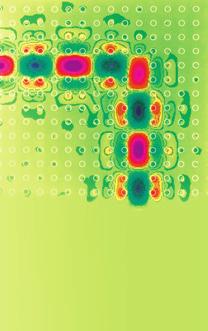
4 4 ISRN Thermodynamics Max: Y Z X Electrical potential (V) Arc-length (μm) Current density (ka/cm 2 ) Figure 5: The current spread in laser diode in different currents. Stripe width and chip width are 1 μmand5μm, respectively. The values of the room temperature thermal conductivities relative temperature dependencies are giving finally in (Wm 1 K 1 ): k GaAs = 44( T ), k InP = k GaP = 77( T 3 ) 1.36, 1 [ (t 3) /111]. To the best of the authors knowledge, there are no published measurements of thermal conductivities relative temperature dependencies in Quaternary AlGaInP compounds. Effective thermal conductivity of a two-layer contact is calculated using the relation k AB = k Ak B (d A +d B ), (7) d A k B +d B k A where k A, k B and d A, d B are the thermal conductivities and the thicknesses, respectively, of both A and B layers. For a three-layer contact, this approach should be repeated [2]. The values of thermal conductivities of contact materials that were used were shown in Table 3. Thermal conductivity of material at room temperature used in simulation was listed in Table 3. This conductivity calculated from the related equations [1]. 4. Simulation Results Figure 6 showsthetemperatureprofileofemitterandheat sink. Figure 6 showsthetopviewtemperatureprofileofthe chip and the temperature difference of regions in the cavity length. There is a temperature difference between 2 regions along the cavity near the front and back mirrors. The reason (6) Temperature ( K) Min: Figure 6: Temperature profile Cavity length (mm) I=25A, P=2W Figure 7: The temperature difference in cavity length and mirror effect. of this difference is for nonsymmetric position on the heat sink in the straight line of cavity (Figure 2). The temperature difference measuring in the cavity length was shown in Figure 7. There are nonlinear differences near mirrors because of mirrorabsorptionandonotherhandthemirrormaterial Al 2 O 3 thermal conduction that is less than cavity material GaAs thermal conduction. The temperature difference in cavity length in different operation currents was shown in Figure 8. The result shows
5 ISRN Thermodynamics Power meter spectrometer Power Wave Fiber connection Detector Temperature ( K) Controller (laser current controller, Peltier current controller, temperature sensors) Laser diode (CS model) Laser beam Integrated sphere 37.5 Figure 1: Experimental arrangement Distance (μm) 25 A 17 A 21 A 14 A Figure 8: The temperature difference in cavity length in different operation currents. Temperature difference ( C) Operation current (A) Figure 9: The wavelength width increasing in different operation currents affected by temperature difference in cavity length. the linear increase in this difference with increase of the operation current (Figure 8). Simulation results for temperature difference in the cavity and the wavelength width variation for this temperature difference was shown in Figure 9.Thewavelengthshiftvalue in single the cavity in simulation is.28 μm/ Cthathas agreement with experimental results which show that this value is.26 μm/ C. 5. Experimental Results The experiment was arranged according to Figure1 and the peak wavelength shift and wavelength width were measured Wavelength width FWHM (nm) Intensity Wavelength (nm) Current =14A (PWL = 85.2 nm) Current =17A (PWL = 86.2 nm) Current =21A (PWL = 87.4 nm) Current =25A (PWL = 88.8 nm) Figure 11: The experimental spectra in different operation currents. in laser diode in different operation currents. The suitable accurate drivers and sensors control the laser current for stable power and TEC (Peltier) current for heat removing. The spectral result was shown in Figure 11. Thereare differences in spectral wavelength width that was shown in Figure 12. The peak wavelength shift value is.26 μm/ C. 6. Result and Conclusion Laser diode peak wavelength was shifted by temperature increase. Our survey about the heat distribution in laser diode shows that there is nonuniform temperature distribution in cavity length of laser diode. This temperature difference increases the spectral wavelength width.
6 6 ISRN Thermodynamics Wavelength width FWHM (nm) Operation current (A) Figure 12: The experimental wavelength width increasing in different operation currents. In this investigation the laser diode CS model was simulated. The result shows that there is 2.5 C difference along cavity length. This difference was increased by increasing operation current. For example, when the operation current was increased from 14 A to 25 A the temperature difference along cavity length was increased from 1 Cto2.7 C; this process increases the wavelength width from 2.2 μm to 2.7 μm. This result was confirmed with experimental results. References [1] B. Laikhtman, A. Gourevitch, D. Donetsky, D. Westerfeld, and G. Belenky, Current spread and overheating of high power laser bars, Applied Physics, vol.95,no.8,pp , 24. [2] A. Tomczyk, R. P. Sarzała, T. Czyszanowski, M. Wasiak, and W. Nakwaski, Fully self-consistent three-dimensional model of edge-emitting nitride diode lasers, Opto-Electronics Review, vol.11,no.1,pp.65 75,23. [3] A. Gourevitch, B. Laikhtman, D. Westerfeld et al., Transient thermal analysis of InGaAsP-InP high-power diode laser arrays with different fill factors, Applied Physics,vol.97,no. 8,ArticleID8453,6pages,25. [4] B. Mroziewicz, M. Bugajski, and W. Nakwaski, Physics of Semiconductor Lasers, North-Holland Science Publishers, [5] F. Bachmann, P. Loosen, and R. Poprawe, High Power Diode Lasers Technology and Applications, Springer, New York, NY, USA, 27. [6] D. S. Patil, Semiconductor Laser Diode Technology and Applications,InTech,Rijeka,Croatia,212. [7] S. Adachi, Properties of Semiconductor Alloys: Group-IV, III V and II VI Semiconductors, John Wiley & Sons, New York, NY, USA, 29. [8] A. Yariv and P. Yeh, Photonics Optical Electronics in Modern Communications,OxfordUniversityPress,NewYork,NY,USA, 27. [9] D. R. Lide, Handbook of Chemistry and Physics, CRCPress, New York, NY, USA, 24.


7 The Scientific World Journal Gravity Photonics Advances in Condensed Matter Physics Soft Matter Aerodynamics Fluids Submit your manuscripts at International International Optics Statistical Mechanics Thermodynamics Computational Methods in Physics Solid State Physics Astrophysics Physics Research International Advances in High Energy Physics International Superconductivity Atomic and Molecular Physics Biophysics Advances in Astronomy
Chapter 5. Semiconductor Laser
 Chapter 5 Semiconductor Laser 5.0 Introduction Laser is an acronym for light amplification by stimulated emission of radiation. Albert Einstein in 1917 showed that the process of stimulated emission must
Metal Vapour Lasers Use vapoured metal as a gain medium Developed by W. Silfvast (1966) Two types: Ionized Metal vapour (He-Cd) Neutral Metal vapour
 Two types: Ionized Metal vapour (He-Cd) Neutral Metal vapour") Metal Vapour Lasers Use vapoured metal as a gain medium Developed by W. Silfvast (1966) Two types: Ionized Metal vapour (He-Cd) Neutral Metal vapour (Cu) All operate by vaporizing metal in container Helium
Metal Vapour Lasers Use vapoured metal as a gain medium Developed by W. Silfvast (1966) Two types: Ionized Metal vapour (He-Cd) Neutral Metal vapour (Cu) All operate by vaporizing metal in container Helium
High Power Diode Lasers
 Lecture 10/1 High Power Diode Lasers Low Power Lasers (below tenth of mw) - Laser as a telecom transmitter; - Laser as a spectroscopic sensor; - Laser as a medical diagnostic tool; - Laser as a write-read
An impact of the electrical pumping scheme on some VCSEL performance characteristics
 Optica Applicata, Vol. XXXIX, No. 4, 2009 An impact of the electrical pumping scheme on some VCSEL performance characteristics SEWERYN MORAWIEC, PIOTR KOWALCZEWSKI, ROBERT P. SARZAŁA * Laboratory of Computer
Electron Energy, E E = 0. Free electron. 3s Band 2p Band Overlapping energy bands. 3p 3s 2p 2s. 2s Band. Electrons. 1s ATOM SOLID.
 Electron Energy, E Free electron Vacuum level 3p 3s 2p 2s 2s Band 3s Band 2p Band Overlapping energy bands Electrons E = 0 1s ATOM 1s SOLID In a metal the various energy bands overlap to give a single
Design and Characterization of InGaAsP/InP and In(Al)GaAsSb/GaSb Laser Diode Arrays
GaAsSb/GaSb Laser Diode Arrays") Design and Characterization of InGaAsP/InP and In(Al)GaAsSb/GaSb Laser Diode Arrays A Dissertation Presented by Alexandre Gourevitch to The Graduate School in Partial fulfillment of the Requirements for
Design and Characterization of InGaAsP/InP and In(Al)GaAsSb/GaSb Laser Diode Arrays A Dissertation Presented by Alexandre Gourevitch to The Graduate School in Partial fulfillment of the Requirements for
Segmented 1.55um Laser with 400% Differential Quantum Efficiency J. Getty, E. Skogen, L. Coldren, University of California, Santa Barbara, CA.
 Segmented 1.55um Laser with 400% Differential Quantum Efficiency J. Getty, E. Skogen, L. Coldren, University of California, Santa Barbara, CA. Abstract: By electrically segmenting, and series-connecting
Emission Spectra of the typical DH laser
 Emission Spectra of the typical DH laser Emission spectra of a perfect laser above the threshold, the laser may approach near-perfect monochromatic emission with a spectra width in the order of 1 to 10
Metal Vapour Lasers Use vapourized metal as a gain medium Developed by W. Silfvast (1966) Put metal in a cavity with a heater Vapourize metal, then
 Put metal in a cavity with a heater Vapourize metal, then") Metal Vapour Lasers Use vapourized metal as a gain medium Developed by W. Silfvast (1966) Put metal in a cavity with a heater Vapourize metal, then pump metal vapour with current Walter at TRG (1966) then
Metal Vapour Lasers Use vapourized metal as a gain medium Developed by W. Silfvast (1966) Put metal in a cavity with a heater Vapourize metal, then pump metal vapour with current Walter at TRG (1966) then
Blue-green Emitting Semiconductor Disk Lasers with Intra-Cavity Frequency Doubling
 Blue-green Emitting Semiconductor Disk Lasers with Intra-Cavity Frequency Doubling Eckart Schiehlen and Michael Riedl Diode-pumped semiconductor disk lasers, also referred to as VECSEL (Vertical External
Study of Steady and Transient Thermal Behavior of High Power Semiconductor Lasers
 Study of Steady and Transient Thermal Behavior of High Power Semiconductor Lasers Zhenbang Yuan a, Jingwei Wang b, Di Wu c, Xu Chen a, Xingsheng Liu b,c a School of Chemical Engineering & Technology of
Signal regeneration - optical amplifiers
 Signal regeneration - optical amplifiers In any atom or solid, the state of the electrons can change by: 1) Stimulated absorption - in the presence of a light wave, a photon is absorbed, the electron is
Semiconductor Disk Laser on Microchannel Cooler
 Semiconductor Disk Laser on Microchannel Cooler Eckart Gerster An optically pumped semiconductor disk laser with a double-band Bragg reflector mirror is presented. This mirror not only reflects the laser
School of Electrical and Computer Engineering, Cornell University. ECE 5330: Semiconductor Optoelectronics. Fall 2014
 School of Electrical and Computer Engineering, Cornell University ECE 5330: Semiconductor Optoelectronics Fall 014 Homework 7 Due on Nov. 06, 014 Suggested Readings: i) Study lecture notes. ii) Study Coldren
Laser Basics. What happens when light (or photon) interact with a matter? Assume photon energy is compatible with energy transition levels.
 interact with a matter? Assume photon energy is compatible with energy transition levels.") What happens when light (or photon) interact with a matter? Assume photon energy is compatible with energy transition levels. Electron energy levels in an hydrogen atom n=5 n=4 - + n=3 n=2 13.6 = [ev]
What happens when light (or photon) interact with a matter? Assume photon energy is compatible with energy transition levels. Electron energy levels in an hydrogen atom n=5 n=4 - + n=3 n=2 13.6 = [ev]
OPTI510R: Photonics. Khanh Kieu College of Optical Sciences, University of Arizona Meinel building R.626
 OPTI510R: Photonics Khanh Kieu College of Optical Sciences, University of Arizona kkieu@optics.arizona.edu Meinel building R.626 Announcements HW #6 is assigned, due April 23 rd Final exam May 2 Semiconductor
Introduction to Optoelectronic Device Simulation by Joachim Piprek
 NUSOD 5 Tutorial MA Introduction to Optoelectronic Device Simulation by Joachim Piprek Outline:. Introduction: VCSEL Example. Electron Energy Bands 3. Drift-Diffusion Model 4. Thermal Model 5. Gain/Absorption
(b) Spontaneous emission. Absorption, spontaneous (random photon) emission and stimulated emission.
 Spontaneous emission. Absorption, spontaneous (random photon) emission and stimulated emission.") Lecture 10 Stimulated Emission Devices Lasers Stimulated emission and light amplification Einstein coefficients Optical fiber amplifiers Gas laser and He-Ne Laser The output spectrum of a gas laser Laser
Lecture 10 Stimulated Emission Devices Lasers Stimulated emission and light amplification Einstein coefficients Optical fiber amplifiers Gas laser and He-Ne Laser The output spectrum of a gas laser Laser
Photoluminescence characterization of quantum dot laser epitaxy
 Photoluminescence characterization of quantum dot laser epitaxy Y. Li *, Y. C. Xin, H. Su and L. F. Lester Center for High Technology Materials, University of New Mexico 1313 Goddard SE, Albuquerque, NM
Chapter 7. Solar Cell
 Chapter 7 Solar Cell 7.0 Introduction Solar cells are useful for both space and terrestrial application. Solar cells furnish the long duration power supply for satellites. It converts sunlight directly
Pressure and Temperature Dependence of Threshold Current in Semiconductor Lasers Based on InGaAs/GaAs Quantum-Well Systems
 Vol. 112 (2007) ACTA PHYSICA POLONICA A No. 2 Proceedings of the XXXVI International School of Semiconducting Compounds, Jaszowiec 2007 Pressure and Temperature Dependence of Threshold Current in Semiconductor
Stimulated Emission Devices: LASERS
 Stimulated Emission Devices: LASERS 1. Stimulated Emission and Photon Amplification E 2 E 2 E 2 hυ hυ hυ In hυ Out hυ E 1 E 1 E 1 (a) Absorption (b) Spontaneous emission (c) Stimulated emission The Principle
Semiconductor Lasers II
 Semiconductor Lasers II Materials and Structures Edited by Eli Kapon Institute of Micro and Optoelectronics Department of Physics Swiss Federal Institute oftechnology, Lausanne OPTICS AND PHOTONICS ACADEMIC
High Speed VCSELs With Separated Quantum Wells
 High Speed VCSELs With Separated Quantum Wells V. V. Lysak 1,2, I. M. Safonov 2, Y. M. Song 1, I. A. Sukhoivanov 1,3, Yong Tak Lee 1 1 Department of Information and Communications, Gwangju Institute of
4 th International Conference on Solid State Crystals. S. MACEGONIUK, R.P. SARZA A, and W. NAKWASKI *
 4 th International Conference on Solid State Crystals OPTO-ELECTRONICS REVIEW 12(4), 389 397 Anticipated performance characteristics of possible InP-based vertical-cavity surface-emitting diode lasers
Defense Technical Information Center Compilation Part Notice
 UNCLSSIFIED Defense Technical Information Center Compilation Part Notice DP013010 TITLE: The Power of Catastrophic Optical Miffor Degradation in InGas/lGas/Gas QW Laser Diodes DISTRIBUTION: pproved for
OPTI510R: Photonics. Khanh Kieu College of Optical Sciences, University of Arizona Meinel building R.626
 OPTI510R: Photonics Khanh Kieu College of Optical Sciences, University of Arizona kkieu@optics.arizona.edu Meinel building R.626 Announcements HW#3 is assigned due Feb. 20 st Mid-term exam Feb 27, 2PM
GaN-based Devices: Physics and Simulation
 GaN-based Devices: Physics and Simulation Joachim Piprek NUSOD Institute Collaborators Prof. Shuji Nakamura, UCSB Prof. Steve DenBaars, UCSB Dr. Stacia Keller, UCSB Dr. Tom Katona, now at S-ET Inc. Dr.
ELECTRONIC DEVICES AND CIRCUITS SUMMARY
 ELECTRONIC DEVICES AND CIRCUITS SUMMARY Classification of Materials: Insulator: An insulator is a material that offers a very low level (or negligible) of conductivity when voltage is applied. Eg: Paper,
Research Article Trial Application of Pulse-Field Magnetization to Magnetically Levitated Conveyor System
 Advances in Condensed Matter Physics Volume 2, Article ID 5657, pages doi:1.1155/2/5657 Research Article Trial Application of Pulse-Field Magnetization to Magnetically Levitated Conveyor System Yoshihito
UNIT I: Electronic Materials.
 SIDDHARTH INSTITUTE OF ENGINEERING & TECHNOLOGY :: PUTTUR Siddharth Nagar, Narayanavanam Road 517583 QUESTION BANK (DESCRIPTIVE) Subject with Code: SEMICONDUCTOR PHYSICS (18HS0851) Course & Branch: B.Tech
Physics of Semiconductors
 Physics of Semiconductors 9 th 2016.6.13 Shingo Katsumoto Department of Physics and Institute for Solid State Physics University of Tokyo Site for uploading answer sheet Outline today Answer to the question
FIBER OPTICS. Prof. R.K. Shevgaonkar. Department of Electrical Engineering. Indian Institute of Technology, Bombay. Lecture: 12.
 FIBER OPTICS Prof. R.K. Shevgaonkar Department of Electrical Engineering Indian Institute of Technology, Bombay Lecture: 12 Optical Sources Fiber Optics, Prof. R.K. Shevgaonkar, Dept. of Electrical Engineering,
Carrier Loss Analysis for Ultraviolet Light-Emitting Diodes
 Carrier Loss Analysis for Ultraviolet Light-Emitting Diodes Joachim Piprek, Thomas Katona, Stacia Keller, Steve DenBaars, and Shuji Nakamura Solid State Lighting and Display Center University of California
EE 6313 Homework Assignments
 EE 6313 Homework Assignments 1. Homework I: Chapter 1: 1.2, 1.5, 1.7, 1.10, 1.12 [Lattice constant only] (Due Sept. 1, 2009). 2. Homework II: Chapter 1, 2: 1.17, 2.1 (a, c) (k = π/a at zone edge), 2.3
LASERS. Dr D. Arun Kumar Assistant Professor Department of Physical Sciences Bannari Amman Institute of Technology Sathyamangalam
 LASERS Dr D. Arun Kumar Assistant Professor Department of Physical Sciences Bannari Amman Institute of Technology Sathyamangalam General Objective To understand the principle, characteristics and types
Research Article Visible Light Communication System Using Silicon Photocell for Energy Gathering and Data Receiving
 Hindawi International Optics Volume 2017, Article ID 6207123, 5 pages https://doi.org/10.1155/2017/6207123 Research Article Visible Light Communication System Using Silicon Photocell for Energy Gathering
Effect of non-uniform distribution of electric field on diffusedquantum well lasers
 Title Effect of non-uniform distribution of electric field on diffusedquantum well lasers Author(s) Man, WM; Yu, SF Citation IEEE Hong Kong Electron Devices Meeting Proceedings, Hong Kong, China, 29 August
Research Article Modeling and Simulation of a Resonant-Cavity-Enhanced InGaAs/GaAs Quantum Dot Photodetector
 Advances in Condensed Matter Physics Volume 215, Article ID 84751, 6 pages http://dx.doi.org/1.1155/215/84751 Research Article Modeling and Simulation of a Resonant-Cavity-Enhanced InGaAs/GaAs Quantum
Semiconductor Laser Based on Thermoelectrophotonics
 University of Central Florida Electronic Theses and Dissertations Doctoral Dissertation (Open Access) Semiconductor Laser Based on Thermoelectrophotonics 2014 Xiaohang Liu University of Central Florida
- Outline. Chapter 4 Optical Source. 4.1 Semiconductor physics
 Chapter 4 Optical Source - Outline 4.1 Semiconductor physics - Energy band - Intrinsic and Extrinsic Material - pn Junctions - Direct and Indirect Band Gaps 4. Light Emitting Diodes (LED) - LED structure
Hybrid indium phosphide-on-silicon nanolaser diode
 In the format provided by the authors and unedited. DOI: 10.1038/NPHOTON.2017.56 Hybrid indium phosphide-on-silicon nanolaser diode Guillaume Crosnier 1,2, Dorian Sanchez 2, Sophie Bouchoule 2, Paul Monnier
Paper Review. Special Topics in Optical Engineering II (15/1) Minkyu Kim. IEEE Journal of Quantum Electronics, Feb 1985
 Minkyu Kim. IEEE Journal of Quantum Electronics, Feb 1985") Paper Review IEEE Journal of Quantum Electronics, Feb 1985 Contents Semiconductor laser review High speed semiconductor laser Parasitic elements limitations Intermodulation products Intensity noise Large
Paper Review IEEE Journal of Quantum Electronics, Feb 1985 Contents Semiconductor laser review High speed semiconductor laser Parasitic elements limitations Intermodulation products Intensity noise Large
HIGH-POWER BIPOLAR AND UNIPOLAR QUANTUM CASCADE LASERS
 HIGH-POWER BIPOLAR AND UNIPOLAR QUANTUM CASCADE LASERS By ARKADIY LYAKH A DISSERTATION PRESENTED TO THE GRADUATE SCHOOL OF THE UNIVERSITY OF FLORIDA IN PARTIAL FULFILLMENT OF THE REQUIREMENTS FOR THE DEGREE
Semiconductor X-Ray Detectors. Tobias Eggert Ketek GmbH
 Semiconductor X-Ray Detectors Tobias Eggert Ketek GmbH Semiconductor X-Ray Detectors Part A Principles of Semiconductor Detectors 1. Basic Principles 2. Typical Applications 3. Planar Technology 4. Read-out
Introduction to semiconductor nanostructures. Peter Kratzer Modern Concepts in Theoretical Physics: Part II Lecture Notes
 Introduction to semiconductor nanostructures Peter Kratzer Modern Concepts in Theoretical Physics: Part II Lecture Notes What is a semiconductor? The Fermi level (chemical potential of the electrons) falls
Impact of the Opto-Geometric Parameters on the Band Diagram and Transmission and Reflection Spectrum of the Bragg Structure
 Optics and Photonics Journal, 2013, 3, 184-189 http://dx.doi.org/10.4236/opj.2013.32030 Published Online June 2013 (http://www.scirp.org/journal/opj) Impact of the Opto-Geometric Parameters on the Band
EE 472 Solutions to some chapter 4 problems
 EE 472 Solutions to some chapter 4 problems 4.4. Erbium doped fiber amplifier An EDFA is pumped at 1480 nm. N1 and N2 are the concentrations of Er 3+ at the levels E 1 and E 2 respectively as shown in
MODELING OF ABOVE-THRESHOLD SINGLE-MODE OPERATION OF EDGE- EMITTING DIODE LASERS
 MODELING OF ABOVE-THRESHOLD SINGLE-MODE OPERATION OF EDGE- EMITTING DIODE LASERS A. P. Napartovich, N. N. Elkin, A. G. Sukharev, V. N. Troshchieva, and D. V. Vysotsky Troitsk Institute for Innovation and
Optical Investigation of the Localization Effect in the Quantum Well Structures
 Department of Physics Shahrood University of Technology Optical Investigation of the Localization Effect in the Quantum Well Structures Hamid Haratizadeh hamid.haratizadeh@gmail.com IPM, SCHOOL OF PHYSICS,
1300nm-Range GaInNAs-Based Quantum Well Lasers with High Characteristic Temperature
 3nm-Range GaInNAs-Based Quantum Well Lasers with High Characteristic Temperature by Hitoshi Shimizu *, Kouji Kumada *, Seiji Uchiyama * and Akihiko Kasukawa * Long wavelength- SQW lasers that include a
Semiconductor Optoelectronics Prof. M. R. Shenoy Department of Physics Indian Institute of Technology, Delhi
 Semiconductor Optoelectronics Prof. M. R. Shenoy Department of Physics Indian Institute of Technology, Delhi Lecture - 1 Context and Scope of the Course (Refer Slide Time: 00:44) Welcome to this course
Nonlinear Time and Temperature Dependent Analysis of the Lead-Free Solder Sealing Ring of a Photonic Switch
 Nonlinear Time and Temperature Dependent Analysis of the Lead-Free Solder Sealing Ring of a Photonic Switch J. Lau, Z. Mei, S. Pang, C. Amsden, J. Rayner and S. Pan Agilent Technologies, Inc. 5301 Stevens
Temperature Dependent Optical Band Gap Measurements of III-V films by Low Temperature Photoluminescence Spectroscopy
 Temperature Dependent Optical Band Gap Measurements of III-V films by Low Temperature Photoluminescence Spectroscopy Linda M. Casson, Francis Ndi and Eric Teboul HORIBA Scientific, 3880 Park Avenue, Edison,
Simulation of AlGaN/Si and InN/Si ELECTRIC DEVICES
 Simulation of AlGaN/Si and InN/Si ELECTRIC DEVICES Zehor Allam 1, Abdelkader Hamdoune 2, Chahrazed Boudaoud 3, Asmaa Amrani 4,Aicha Soufi 5,Zakia Nakoul 6 Unity of Research Materials and Renewable Energies,
How to measure packaging-induced strain in high-brightness diode lasers?
 How to measure packaging-induced strain in high-brightness diode lasers? Jens W. Tomm Max-Born-Institut für Nichtlineare Optik und Kurzzeitspektroskopie Berlin Max-Born-Str. 2 A, D-12489 Berlin, Germany
Laser Diodes. Revised: 3/14/14 14: , Henry Zmuda Set 6a Laser Diodes 1
 Laser Diodes Revised: 3/14/14 14:03 2014, Henry Zmuda Set 6a Laser Diodes 1 Semiconductor Lasers The simplest laser of all. 2014, Henry Zmuda Set 6a Laser Diodes 2 Semiconductor Lasers 1. Homojunction
Near-Infrared Spectroscopy of Nitride Heterostructures EMILY FINAN ADVISOR: DR. OANA MALIS PURDUE UNIVERSITY REU PROGRAM AUGUST 2, 2012
 Near-Infrared Spectroscopy of Nitride Heterostructures EMILY FINAN ADVISOR: DR. OANA MALIS PURDUE UNIVERSITY REU PROGRAM AUGUST 2, 2012 Introduction Experimental Condensed Matter Research Study of large
Ms. Monika Srivastava Doctoral Scholar, AMR Group of Dr. Anurag Srivastava ABV-IIITM, Gwalior
 By Ms. Monika Srivastava Doctoral Scholar, AMR Group of Dr. Anurag Srivastava ABV-IIITM, Gwalior Unit 2 Laser acronym Laser Vs ordinary light Characteristics of lasers Different processes involved in lasers
Quantum Dot Lasers. Jose Mayen ECE 355
 Quantum Dot Lasers Jose Mayen ECE 355 Overview of Presentation Quantum Dots Operation Principles Fabrication of Q-dot lasers Advantages over other lasers Characteristics of Q-dot laser Types of Q-dot lasers
OPTI510R: Photonics. Khanh Kieu College of Optical Sciences, University of Arizona Meinel building R.626
 OPTI510R: Photonics Khanh Kieu College of Optical Sciences, University of Arizona kkieu@optics.arizona.edu Meinel building R.626 Announcements Homework #6 is assigned, due May 1 st Final exam May 8, 10:30-12:30pm
Unit IV Semiconductors Engineering Physics
 Introduction A semiconductor is a material that has a resistivity lies between that of a conductor and an insulator. The conductivity of a semiconductor material can be varied under an external electrical
Simulation of GaN-based Light-Emitting Devices
 Simulation of GaN-based Light-Emitting Devices Joachim Piprek Solid-State Lighting and Display Center Materials Department, College of Engineering University of California, Santa Barbara, CA 93106 piprek@ieee.org
ISSN Review. Progress to a Gallium-Arsenide Deep-Center Laser
 Materials 2009, 2, 1599-1635; doi:10.3390/ma2041599 OPEN ACCESS materials ISSN 1996-1944 www.mdpi.com/journal/materials Review Progress to a Gallium-Arsenide Deep-Center Laser Janet L. Pan Yale University,
Study on Quantum Dot Lasers and their advantages
 Study on Quantum Dot Lasers and their advantages Tae Woo Kim Electrical and Computer Engineering University of Illinois, Urbana Champaign Abstract Basic ideas for understanding a Quantum Dot Laser were
PHOTOVOLTAICS Fundamentals
 PHOTOVOLTAICS Fundamentals PV FUNDAMENTALS Semiconductor basics pn junction Solar cell operation Design of silicon solar cell SEMICONDUCTOR BASICS Allowed energy bands Valence and conduction band Fermi
Research Article Noncontact Measurement for Radius of Curvature of Unpolished Lens
 International Optics, Article ID 3403, 7 pages http://dx.doi.org/10.1155/014/3403 Research Article Noncontact Measurement for Radius of Curvature of Unpolished Lens Haifeng Liang College of Photoelectrical
Research Article Temperature Dependence of the Raman Frequency of an Internal Mode for SiO 2 -Moganite Close to the α-β Transition
 Thermodynamics Volume 2012, Article ID 892696, 4 pages doi:10.1155/2012/892696 Research Article Temperature Dependence of the Raman Frequency of an Internal Mode for SiO 2 -Moganite Close to the α-β Transition
Review Article Nanoparticle Imaging with Polarization Interferometric Nonlinear Confocal Microscope
 Advances in Condensed Matter Physics, Article ID 176862, 6 pages http://dx.doi.org/10.1155/2014/176862 Review Article Nanoparticle Imaging with Polarization Interferometric Nonlinear Confocal Microscope
School of Electrical and Computer Engineering, Cornell University. ECE 5330: Semiconductor Optoelectronics. Fall Due on Nov 20, 2014 by 5:00 PM
 School of Electrical and Computer Engineering, Cornell University ECE 533: Semiconductor Optoelectronics Fall 14 Homewor 8 Due on Nov, 14 by 5: PM This is a long -wee homewor (start early). It will count
Research Article Emissivity Measurement of Semitransparent Textiles
 Advances in Optical Technologies Volume 2012, Article ID 373926, 5 pages doi:10.1155/2012/373926 Research Article Emissivity Measurement of Semitransparent Textiles P. Bison, A. Bortolin, G. Cadelano,
Classification of Solids
 Classification of Solids Classification by conductivity, which is related to the band structure: (Filled bands are shown dark; D(E) = Density of states) Class Electron Density Density of States D(E) Examples
Appendix. Photonic crystal lasers: future integrated devices
 91 Appendix Photonic crystal lasers: future integrated devices 5.1 Introduction The technology of photonic crystals has produced a large variety of new devices. However, photonic crystals have not been
Thermal performance investigation of DQW GaInNAs laser diodes
 Thermal performance investigation of DQW GaInNAs laser diodes Jun Jun Lim, Roderick MacKenzie, Slawomir Sujecki, Eric Larkins Photonic and Radio Frequency Engineering Group, School of Electrical and Electronic
Designing a high speed 1310nm AlGaInAs/AlGaInAs VCSEL using MgO/Si top DBR and GaInAsP/InP bottom DBR
 American Journal of Optics and Photonics 014; (3): 37-44 Published online July 0, 014 (http://www.sciencepublishinggroup.com/j/ajop) doi: 10.11648/j.ajop.014003.14 ISSN: 330-8486 (Print); ISSN: 330-8494
Solar cells operation
 Solar cells operation photovoltaic effect light and dark V characteristics effect of intensity effect of temperature efficiency efficency losses reflection recombination carrier collection and quantum
Course overview. Me: Dr Luke Wilson. The course: Physics and applications of semiconductors. Office: E17 open door policy
 Course overview Me: Dr Luke Wilson Office: E17 open door policy email: luke.wilson@sheffield.ac.uk The course: Physics and applications of semiconductors 10 lectures aim is to allow time for at least one
Final Exam Solution, Spring Semester 2011 ECSE 6962, Light Emitting Diodes and Solid State Lighting (Prof. E. F. Schubert)
") Final Exam Solution, Spring Semester 2011 ECSE 6962, Light Emitting Diodes and Solid State Lighting (Prof. E. F. Schubert) Note: Put your name on your paper. Show your work. Underline all results. Always
Final Exam Solution, Spring Semester 2011 ECSE 6962, Light Emitting Diodes and Solid State Lighting (Prof. E. F. Schubert) Note: Put your name on your paper. Show your work. Underline all results. Always
Photonic Devices. Light absorption and emission. Transitions between discrete states
 Light absorption and emission Photonic Devices Transitions between discrete states Transition rate determined by the two states: Fermi s golden rule Absorption and emission of a semiconductor Vertical
R. Ludwig and G. Bogdanov RF Circuit Design: Theory and Applications 2 nd edition. Figures for Chapter 6
 R. Ludwig and G. Bogdanov RF Circuit Design: Theory and Applications 2 nd edition Figures for Chapter 6 Free electron Conduction band Hole W g W C Forbidden Band or Bandgap W V Electron energy Hole Valence
Optoelectronics ELEC-E3210
 Optoelectronics ELEC-E3210 Lecture 3 Spring 2017 Semiconductor lasers I Outline 1 Introduction 2 The Fabry-Pérot laser 3 Transparency and threshold current 4 Heterostructure laser 5 Power output and linewidth
MSE 310/ECE 340: Electrical Properties of Materials Fall 2014 Department of Materials Science and Engineering Boise State University
 MSE 310/ECE 340: Electrical Properties of Materials Fall 2014 Department of Materials Science and Engineering Boise State University Practice Final Exam 1 Read the questions carefully Label all figures
Enhancing the Rate of Spontaneous Emission in Active Core-Shell Nanowire Resonators
 Chapter 6 Enhancing the Rate of Spontaneous Emission in Active Core-Shell Nanowire Resonators 6.1 Introduction Researchers have devoted considerable effort to enhancing light emission from semiconductors
InGaAs-AlAsSb quantum cascade lasers
 InGaAs-AlAsSb quantum cascade lasers D.G.Revin, L.R.Wilson, E.A.Zibik, R.P.Green, J.W.Cockburn Department of Physics and Astronomy, University of Sheffield, UK M.J.Steer, R.J.Airey EPSRC National Centre
The Report of the Characteristics of Semiconductor Laser Experiment
 The Report of the Characteristics of Semiconductor Laser Experiment Masruri Masruri (186520) 22/05/2008 1 Laboratory Setup The experiment consists of two kind of tasks: To measure the caracteristics of
Understanding Semiconductor Lasers
 27 April 2010 age 1 of 8 Experiment II Understanding Semiconductor Lasers The purpose of this experiment is to explore the basic characteristics of semiconductor lasers. We will measure and calculate the
Modeling Internal Heating of Optoelectronic Devices Using COMSOL
 Modeling Internal Heating of Optoelectronic Devices Using COMSOL Nathan Brunner 1,2 1 Voxtel, Inc. Beaverton, OR*; 2 Department of Physics, University of Oregon, Eugene, OR *nathanb@voxtel-inc.com, 15985
Lecture 2. Introduction to semiconductors Structures and characteristics in semiconductors
 Lecture 2 Introduction to semiconductors Structures and characteristics in semiconductors Semiconductor p-n junction Metal Oxide Silicon structure Semiconductor contact Literature Glen F. Knoll, Radiation
VALLIAMMAI ENGINEERING COLLEGE
 VALLIAMMAI ENGINEERING COLLEGE SRM Nagar, Kattankulathur 603 203 DEPARTMENT OF PHYSICS QUESTION BANK II SEMESTER PH8252 - PHYSICS FOR INFORMATION SCIENCE (Common to CSE & IT) Regulation 2017 Academic Year
Optical Self-Organization in Semiconductor Lasers Spatio-temporal Dynamics for All-Optical Processing
 Optical Self-Organization in Semiconductor Lasers Spatio-temporal Dynamics for All-Optical Processing Self-Organization for all-optical processing What is at stake? Cavity solitons have a double concern
A semiconductor is an almost insulating material, in which by contamination (doping) positive or negative charge carriers can be introduced.
 positive or negative charge carriers can be introduced.") Semiconductor A semiconductor is an almost insulating material, in which by contamination (doping) positive or negative charge carriers can be introduced. Page 2 Semiconductor materials Page 3 Energy levels
Semiconductor A semiconductor is an almost insulating material, in which by contamination (doping) positive or negative charge carriers can be introduced. Page 2 Semiconductor materials Page 3 Energy levels
THz QCL sources based on intracavity difference-frequency mixing
 THz QCL sources based on intracavity difference-frequency mixing Mikhail Belkin Department of Electrical and Computer Engineering The University of Texas at Austin IQCLSW, Sept. 3, 218 Problems with traditional
Review Article Numerical Self-Consistent Analysis of VCSELs
 Advances in Optical Technologies Volume 202, Article ID 68959, 7 pages doi:0.55/202/68959 Review Article Numerical Self-Consistent Analysis of VCSELs Robert Sarzała, Tomasz Czyszanowski, Michał Wasiak,
Sheng S. Li. Semiconductor Physical Electronics. Second Edition. With 230 Figures. 4) Springer
 Springer") Sheng S. Li Semiconductor Physical Electronics Second Edition With 230 Figures 4) Springer Contents Preface 1. Classification of Solids and Crystal Structure 1 1.1 Introduction 1 1.2 The Bravais Lattice
Sheng S. Li Semiconductor Physical Electronics Second Edition With 230 Figures 4) Springer Contents Preface 1. Classification of Solids and Crystal Structure 1 1.1 Introduction 1 1.2 The Bravais Lattice
Electroluminescence from Silicon and Germanium Nanostructures
 Electroluminescence from silicon Silicon Getnet M. and Ghoshal S.K 35 ORIGINAL ARTICLE Electroluminescence from Silicon and Germanium Nanostructures Getnet Melese* and Ghoshal S. K.** Abstract Silicon
Temperature dependence of wall-plug efficiency of high power laser diodes
 Vol. 8(10), pp. 36-370, 16 March, 013 DOI: 10.5897/IJPS1.615 ISSN 199-1950 013 Academic Journals http://www.academicjournals.org/ijps International Journal of Physical Sciences Full Length Research Paper
Research Article Generalized Analytical Solutions for Nonlinear Positive-Negative Index Couplers
 Physics Research International Volume, Article ID 9587, pages doi:.55//9587 Research Article Generalized Analytical Solutions for Nonlinear Positive-Negative Index Couplers Zh. Kudyshev,, G. Venugopal,
PH575 Spring Lecture #20 Semiconductors: optical properties: Kittel Ch. 8 pp ; Ch 15 pp
 PH575 Spring 2014 Lecture #20 Semiconductors: optical properties: Kittel Ch. 8 pp. 187-191; Ch 15 pp. 435-444 Figure VI-1-1: Different types of optical absorption phenomena; (1) transitions of highlying
ρ ρ LED access resistances d A W d s n s p p p W the output window size p-layer d p series access resistance d n n-layer series access resistance
 LED access resistances W the output window size p-layer series access resistance d p n-layer series access resistance d n The n-layer series access resistance R = ρ s n where the resistivity of the n-layer