Near-field radiative heat transfer devices
|
|
|
- Johnathan Burke
- 5 years ago
- Views:
Transcription
1 Near-field radiative heat transfer devices John DeSutter 1, Lei Tang 2, and Mathieu Francoeur 1,* 1 Radiative Energy Transfer Lab, Department of Mechanical Engineering, University of Utah, Salt Lake City, UT 84112, USA 2 Department of Mechanical Engineering, University of California, Berkeley, Berkeley, CA 94720, USA Recently, many works have experimentally demonstrated near-field radiative heat transfer (NFRHT) exceeding the far-field blackbody limit between planar surfaces Due to the difficulties associated with maintaining the nanosize gaps required for measuring a nearfield enhancement, these demonstrations have been limited to experiments that cannot be implemented into actual applications. This poses a significant bottleneck to the advancement of NFRHT research. Here, we describe devices bridging laboratory-scale measurements and potential NFRHT engineering applications in energy conversion 16,17 and thermal management We report a maximum NFRHT enhancement of ~ 28.5 over the blackbody limit with devices made of millimeter-sized doped silicon (Si) surfaces separated by vacuum gap spacings down to ~ 110 nm. The devices capitalize on micropillars, separating the high-temperature emitter and low-temperature receiver, manufactured within micrometer-deep pits. These micropillars, which are ~ 4.5 to 45 times longer than the nanosize vacuum spacing where radiation transfer takes place, minimize parasitic heat conduction without sacrificing device structural integrity. The robustness of our devices enables gap spacing visualization via scanning electron microscopy (SEM) prior to * mfrancoeur@mech.utah.edu 1
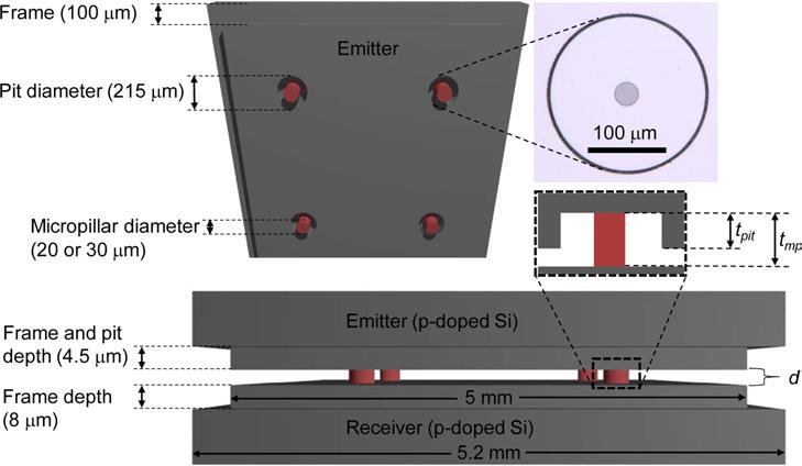
2 performing NFRHT measurements. Direct gap spacing characterization is critical for transitioning NFRHT research from laboratory-scale experiments to applications. In the near field (i.e., subwavelength vacuum gap spacing), tunneling of evanescent modes allows for radiative heat transfer to exceed Planck s far-field blackbody limit by orders of magnitude 21. While NFRHT research is primarily motivated by potential performance enhancement in energy conversion and thermal management technologies, NFRHT devices that can be implemented into engineering applications are yet to be realized. Precision alignment systems 1 6,17,20 are well-suited for laboratory demonstration of NFRHT, but integration of such systems into actual applications is not feasible. Measurements of NFRHT between surfaces separated by micro/nanosize vacuum gap spacings supported by particle 7,8 or microfabricated 9 11,18 spacers and via microelectromechanical systems 12 15,19 have been performed. However, significant thermal conduction 8 11,18 between the emitter and receiver greatly reduces the effectiveness of any potential devices capitalizing on NFRHT. Fragile and intricate structures are difficult to manufacture and characterize 15. Devices requiring external forces 12 15,19 to maintain desired nanosize gap spacings further characterization difficulties and greatly complicate practical implementation. Finally, surfaces of microsize dimensions 12,13,19 severely limit the total radiative heat exchange. We circumvent these limitations by fabricating and characterizing bonded devices suitable for potential engineering applications of NFRHT. These devices independently support their own gap spacing (standalone), have surfaces with macroscale dimensions, minimize parasitic heat conduction, and their structural integrity enables gap spacing visualization via SEM. A NFRHT device, manufactured using standard micro/nanofabrication techniques as detailed in Methods and Supplementary Fig. 1, is shown in Fig. 1a. It consists of a high-temperature emitter 2
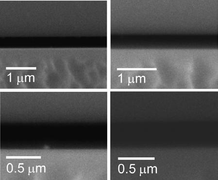
3 and low-temperature receiver made of Si, with boron doping of ~ cm -3, separated by low thermal conductivity SU micropillars (0.2 Wm -1 K -1 ) 22 having diameters of either ~ 20 or 30 µm. Both emitter and receiver are 525-µm-thick, have surface area of mm 2, and are characterized by RMS surface roughness of less than 0.2 nm as provided by the manufacturer (Silicon Valley Microelectronics). Approximately 4.5-µm-deep, 215-µm-diameter pits are etched into the emitter substrate where the micropillars are manufactured. The pits enable devices with micropillars significantly longer than the nominal gap spacing, d, between the emitter and receiver, thus minimizing the contribution of parasitic conduction to the total heat rate. The micropillar and pit areas respectively cover 0.01% and less than 1.2% of the total surface of the device. A 100-µm-wide frame is etched into both the emitter and receiver substrates to prevent particle contamination at the edges of the device, due to dicing and handling, from interfering with the desired gap spacing. On the emitter side, the frame is etched to the same depth as the pits while the receiver frame is ~ 8-µm-deep. The resulting separation distance between the emitter and receiver along the edges of the device is greater than 12.5 µm, which is much larger than most particles. After meticulously cleaning the emitter and receiver (see Methods), the micropillars are bonded to the receiver surface. The robustness of the fabricated NFRHT devices enables imaging of the gap spacing d via SEM. Figure 1b shows SEM images of gap spacing at the four corners of a device with d 380 nm. SEM images allow direct gap spacing characterization prior to performing heat transfer measurements. Heat transfer measurements are conducted using the setup shown in Fig. 1c located inside a vacuum chamber (P < Pa) housed in a class 1000 cleanroom tent. The emitter is heated by a thermoelectric heat pump (Custom Thermoelectric, B30-22RU4) while the receiver temperature is held constant at ~ 300 K via a thermoelectric cooler (TETechnology, VT
4 1.3). The heat rate across the device, due to radiation heat transfer (Q rad ) and conduction heat transfer through the micropillars (Q cond ), is measured with a custom built mm 2 heat flux meter (HFM) from FluxTeq (PHFS-JD10). Two thermistors (Selco, LSMC700A010KD002), one embedded in a 0.5-mm-thick, 5 5 mm 2 copper heat spreader located between the heat pump and emitter (T h ) and one embedded in an identical heat spreader placed directly under the receiver (T l ), are used to measure the temperature difference across the device. Additional 0.5- mm-thick, mm 2 copper heat spreaders surround the HFM to ensure uniform flux across the meter. Contact resistance is minimized by applying thermal grease (Arctic Silver Ceramique 2) at all interfaces. The resulting thermal resistance between T h and T e, and T l and T r are ~ 4.75 KW -1, where T e and T r are the emitter and receiver temperatures adjacent to the vacuum gap (see Supplementary Section 1). Heat transfer measurements are calibrated using 1.1-mm-thick, 5 5 mm 2 samples of soda lime glass with known thermal conductivity of 0.94 Wm -1 K -1 ; HFM calibration is detailed in Supplementary Section 1 and Supplementary Fig. 2. Fig. 2a compares theoretical and experimental near-field radiative heat flux, q rad, for six devices with varying vacuum gap spacings and temperature differences ΔT = T e T r (T r = 300 ± 0.5 K) ranging from ~ 5 to 100 K (radiation from the pits and frame is not included). SEM images of the gap spacing at the four corners of each device are provided in Supplementary Fig. 3. The gap spacing range provided in the legend of Fig. 2a for a specific device is determined from the SEM images, and a thermal and structural analysis of the device (see Supplementary Section 2). For example, the gap spacing at each corner of the device leading to the largest radiative flux is estimated to be 92, 109, 114, and 122 nm at room temperature. Theoretical radiative flux is calculated using fluctuational electrodynamics 21,23 (FE) (see Methods). The radiative flux associated with a specific device is calculated as the average of four radiative fluxes computed at 4
5 the four gap spacings derived from SEM imaging. The colored theoretical bands arise from uncertainty in the vacuum gap spacing extracted from SEM images, Si doping levels, and micropillar height and diameter (see Methods for uncertainty analysis). Theoretical and experimental trends are in good agreement, and the radiative flux measured for all devices exceeds the far-field blackbody limit. A maximum conduction contribution of ~ 22 to 35% is estimated for the largest gap device ( nm), while the conduction contribution reaches a minimum of ~ 1.9 to 4.1% for the smallest gap device ( nm). The radiative heat transfer coefficient, h rad, and the enhancement over the blackbody limit, E BB, are shown in Fig. 2b as a function of the vacuum gap spacing for a temperature difference of 70 ± 2 K. The device with the smallest gap spacing is characterized by a h rad value of ~ 247 Wm -2 K -1, which falls within the upper range of forced convection with gases. This leads to a substantial radiative transfer enhancement over the blackbody limit, E BB, of approximately Unprocessed heat rate data that includes radiative transfer between the emitter and receiver separated by a gap spacing d, radiative transfer from the bottom of the pits and frame (recessed areas) to the receiver, and conduction through the micropillars are provided in Supplementary Fig. 4. Near-field enhancement is explained by analyzing the radiative flux as a function of the angular frequency, ω, and wavevector parallel to the emitter and receiver surfaces, k ρ, for devices with the largest and smallest gap spacing, and a temperature difference of 70 K (see Fig. 3a). In transverse magnetic polarization, doped Si supports surface plasmon-polaritons (SPPs) characterized by large parallel wavevectors k ρ exceeding the material light line Re(n)k 0, where n is the refractive index of doped Si and k 0 is the magnitude of the wavevector in vacuum 24. For reference, the SPP dispersion relation (ω + and ω ) in the Si-vacuum-Si configuration is plotted in Fig. 3a (see Methods). In the electrostatic limit, the largest contributing parallel wavevector to 5
6 the flux for doped Si supporting SPPs in the infrared is estimated as k ρ d For the smallest gap device (calculated here as d = 110 nm), the flux is dominated by SPPs evanescent in both vacuum and Si with k ρ greatly exceeding the material light line (~ 82% of the flux is due to SPPs). This is also observed in Fig. 3b, where the monochromatic flux for the smallest gap device is maximum near the resonant frequency of a Si-vacuum interface ω SPP ω p / ε +1 = rad/s, where ω p is the plasma frequency (= rad/s) and ε is the limiting value of the dielectric function at high frequency (= 11.7) (see Supplementary Section 3). SPP resonance of a Si-vacuum interface is derived by assuming the materials are lossless, which explains the small discrepancy with FE predictions in Fig. 3b. For the largest gap device (calculated here as d = 1000 nm), the flux is still dominated by evanescent modes in vacuum (~ 73% of the flux is due to evanescent modes). The largest contribution comes from frustrated modes (~ 53% of the flux), characterized by parallel wavevectors k 0 < k ρ < Re(n)k 0, that are propagating in Si but evanescent in vacuum (see Fig. 3a). This leads to a broadband enhancement of the flux, as opposed to the narrowband enhancement mediated by thermal excitation of SPPs obtained with the smallest gap device (see Fig. 3b). The biggest challenge in transitioning NFRHT from laboratory-scale experiments to engineering applications is fabricating standalone, structurally robust devices while minimizing the relative contribution of conduction to the total heat rate. Our devices overcome this challenge by manufacturing micropillars, separating the emitter and receiver, inside micrometer-deep pits. Extending micropillar height to a few micrometers while keeping the gap spacing, d, in the range ~ 100 to 1000 nm substantially increases the thermal resistance by conduction, R cond, between the emitter and receiver. For example, conduction heat transfer is reduced by a factor of ~ 42 when 6
7 comparing a 110-nm-gap device without pits to the same device with 4.5-µm-deep pits. For our smallest gap device leading to a NFRHT enhancement of ~ 28.5 beyond the blackbody limit, the contribution of conduction to the total heat rate would increase from ~ 1.9% with pits to 45% without pits. Despite the large enhancement of NFRHT, a pit-free-device would be unusable for applications such as thermophotovoltaic energy conversion where heat conduction is detrimental to device performance 26. Micropillars with relatively large diameters, (here, 20 to 30 µm) ensuring device structural integrity without having the drawback of large parasitic heat conduction, can be fabricated by capitalizing on micrometer-deep pits. Such structural integrity enables direct gap spacing characterization via SEM, which is critical in assessing the quality of our NFRHT devices. To our knowledge, this is the first time nanoscale gap spacings have been imaged in the context of NFRHT across macroscale surfaces with both lateral dimensions exceeding 1 mm. Measurement of NFRHT across macroscale planar surfaces at a gap spacing as small as ~ 110 nm has never been reported. Here, the impact of surface area cannot be understated. While it is easier to maintain sub-100-nm vacuum gap spacing between microsize surfaces due to simpler parallelization and decreased likelihood of surface defects and contamination, the radiative heat rate is severely limited. For instance, despite achieving a gap spacing of ~ 25 nm across microsize planar surfaces, the radiative heat rate in our smallest gap device is ~ 300 times larger than that reported in Ref. 4 for a temperature difference of ~ 10 K. In vacuum, a blackbody provides an upper limit for radiative heat transfer in the wavevector range k ρ < k 0. Therefore, the only way to transfer radiation exceeding the blackbody limit across a vacuum gap is by tunneling evanescent modes with k ρ > k 0. This is, indeed, possible in the near field. 21 In the far field, evanescent modes cannot contribute to radiative transfer and wavevectors 7
8 are limited to k ρ < k 0. As such, far-field radiative heat transfer exceeding the blackbody limit, as claimed in Ref. 27, is not physically possible The NFRHT devices proposed here are, therefore, critical for the development and implementation of applications capitalizing on radiation transfer exceeding the blackbody limit. In summary, we successfully fabricated and characterized NFRHT devices with gap spacings from ~ 1000 nm down to ~ 110 nm separating millimeter-sized surfaces of doped Si. Our singular design capitalizes on long micropillars, manufactured inside micrometer-deep pits, minimizing parasitic heat conduction without sacrificing structural integrity. These devices constitute a critical step towards realizing potential NFRHT applications in energy conversion and thermal management. The NFRHT devices described here cannot be operated at temperatures higher than ~ 450 K 31 due to instability of SU-8. However, by keeping the same design and by adjusting the fabrication process (e.g., hybrid SU-8/SiO 2 micropillars), we anticipate that the proposed devices can sustain temperature differences exceeding 1000 K. 8
9 Methods Device fabrication and cleanliness. The main steps required for fabricating NFRHT devices are shown in Supplementary Fig. 1. The 100-mm-diameter Si wafers used for both the emitter and receiver, purchased from Silicon Valley Microelectronics, are characterized by bow smaller than 4.5 µm. Throughout the entire process, emitter and receiver surfaces are only exposed to class 100 or 1000 cleanroom environments. The emitter is fabricated by first spinning on a thick (~ 15 µm) layer of AZ 9260 photoresist (PR) (step 1). Pit and frame pattern generation is achieved by exposing the AZ 9260 PR to UV light shadowed by a photomask in a Suss MA1006 mask aligner (step 2). The pits and frame are then etched to a depth of approximately 4.5 µm using a CF 4 O 2 reactive ion etch (RIE) in an Oxford Plasmalab 80 for 1 hour and 50 minutes (step 3). The frame is implemented into device design to minimize the impact of debris from dicing and handling. The dicing saw can produce significant particle contamination that is primarily concentrated near the sample edges. Therefore, the recessed frames prevents the majority of this debris from interfering with the desired gap spacing, d. The masking AZ 9260 layer is then removed using acetone, isopropanol (IPA), and a short O 2 RIE. SU permanent photoresist is then spin-coated with two different spin settings (step 4). Spin 1 is for 8 seconds at 500 rpm with a ramp rate of 100 rpm/s. Spin 2 is for 35 seconds at 2650 rpm with a ramp rate of 300 rpm/s. This is immediately followed by a soft bake at 95 C for 135 seconds. 5.5 to 6.5-µm-thick SU-8 micropillars are patterned (step 5) via exposure to 120 mj of UV radiation shadowed by a photomask. To produce micropillars with flat surfaces, a post exposure bake (PEB) at 70 C for 1 minute preludes a PEB at 95 C for 1 minute. The SU-8 is developed for 2 minutes. The emitter pattern is then cut into mm 2 die using a Disco DAD641 dicing saw. To help avoid Si debris while dicing, a thick (10 15 µm) protective AZ 9260 PR layer is deposited onto the 9
10 emitter wafer (step 6) and dicing tape is then adhered on the protective layer. The receiver frame is patterned and diced using a similar procedure to that of the emitter (see steps 7 to 10 in Supplementary Fig. 1). After dicing, the tape and AZ 9260 are removed in a sonicated acetone bath for 1 minute (step 11). Once the tape is removed, the samples are immediately moved to a second sonicated acetone bath for 5 minutes. This is followed by 1 minute IPA and deionized (DI) water sonicated baths. Micropillar height is characterized using a Tencor p-20 profilometer. To achieve desired height and uniformity, the micropillars are selectively etched in an O 2 plasma while using a suspended shadowmask (step 12). Shorter micropillars are shadowed resulting in a slower etch rate. The iterative process of profilometer characterization and O 2 plasma etching is carried out until micropillars have the desired height and a uniformity less than 20 nm. The surfaces of both the emitter and receiver must be pristine prior to bonding. If there is debris on the surfaces when viewed through an Olympus MX51 microscope once the micropillars have the desired height and uniformity, the edges of the top surfaces of the emitter and receiver are wiped with a cleanroom cloth (CONTEC Polywipe-C) soaked in IPA. The samples are then sprayed with acetone, IPA, and DI water to remove any additional debris the cloth may have left. This is another iterative process involving sample inspection in the Olympus microscope and the wipe/spray cleaning procedure that is undertaken until no visible particles are detected on the emitter and receiver surfaces. This is a delicate process as wiping the micropillars must be avoided. The emitter and receiver are then aligned using a square alignment fixture and bonded in an oven for 30 minutes at 200 C (step 13). No additional pressure is applied to the device during the bonding process. 10
11 Heat transfer calculations. NFRHT is modeled using FE 21,23. The propagating, q prop rad, and evanescent, q evan rad, components of the radiative flux are calculated as follows for two infinite planes separated by a vacuum gap spacing d: k 0 τ ( ) 2 1 r τ 2 0r ( ) q prop rad = 1 1 r 0e dω[θ(ω,t 4π 2 e ) Θ(ω,T r )] dk ρ (1) 0 1 r τ 0e r τ 0r e 2i Re(k z 0 )d 2 0 τ =TE,TM q evan rad = 1 Im(r dω[θ(ω,t π τ 2 e ) Θ(ω,T r )] dk ρ k ρ e 2Im(k z 0 )d 0e )Im(r τ 0r ) (2) 0 1 r τ 0e r τ 0r e 2Im(k z 0 )d 2 k τ =TE,TM 0 where the subscripts 0, e, and r respectively refer to vacuum, emitter, and receiver. In Eqs. (1) and (2), Θ(ω,T) is the mean energy of an electromagnetic state, k z0 is the component of the τ vacuum wavevector perpendicular to an interface, and r 0e,r is the Fresnel reflection coefficient at the vacuum/emitter (e) or vacuum/receiver (r) interface in polarization state τ. The radiative flux used for generating the results in Fig. 2a and Supplementary Fig. 4 is the sum of Eqs. (1) and (2). The data in Fig. 3a is generated by solving Eqs. (1) and (2) per unit angular frequency, ω, and per unit parallel wavevector, k ρ (i.e., both integrations are dropped). The spectral radiative flux in Fig. 3b is produced by solving Eqs. (1) and (2) per unit angular frequency, ω (i.e., the integration over ω is dropped). For a specific device, the radiative flux, q rad, is calculated as the average of four radiative fluxes computed using the gap spacing at each of the four corners of the device derived from SEM imaging. To calculate the radiative flux between the recessed areas (bottom of pits and frame) in the emitter and receiver, Eqs. (1) and (2) are used again, but with a gap spacing t mp = t pit + d avg for 11
12 the pits and t frame = 12.5 µm + d avg for the frame (see Fig. 1a), where d avg is the average gap spacing of the four measured corners. These equations assume a view factor of unity, which is an excellent approximation for the emitter-receiver portion of the device separated by a vacuum gap spacing, d. It is less accurate for the recessed areas where two-dimensional (2D) effects may be relevant. The area of the pits and frame accounts for less than 9% of the total device surface area. For the largest gap device ( nm), ~ 97% of the radiative heat rate is due to radiation exchange across the gap spacing, d. The largest gap device is more impacted by the pit and frame radiative transfer than any of the other devices investigated. Therefore, accounting for potential 2D effects is clearly not necessary. One-dimensional, steady-state conduction through the SU-8 micropillars with thickness t mp is considered. This is justified by the fact that the micropillar temperature is uniform in the direction parallel to the Si surfaces. A temperature-independent thermal conductivity of 0.2 Wm - 1 K -1 for SU-8 is used in the calculations 22. Contact resistances at the SU-8/Si interfaces are neglected since SU-8 reflows and fills voids during the bonding process. Uncertainty analysis Experimental data. Each experimental point consists of the average value of a set of data recorded by the HFM every second for at least two minutes once steady state is reached. The distribution uncertainty associated with a set of data is calculated by taking two standard deviations of the mean. The accuracy uncertainty of 5% is provided by the HFM manufacturer. These uncertainties are added together to obtain the total heat rate uncertainty. The heat rate is ± W for the case of largest uncertainty (smallest gap device, largest temperature difference) and ± W for the case of smallest uncertainty (largest gap device, smallest temperature difference). 12
13 Twenty-four measurements of thermal grease resistance (R grease ) between the hot-side thermistor, T h, and T e and the cold-side thermistor, T l, and T r (see Fig. 1c) were taken (see Supplementary Section 1). The uncertainty in these measurements is the difference between the maximum and minimum recorded values. Thermal grease resistance uncertainty has the largest influence on temperature uncertainty, which also considers the ± 0.1 K accuracy of each thermistor and the ± (0.2 % + 1 Ω) accuracy of the LCR meter (BK Precision 889B). The temperature difference is 78.6 ± 1.8 K for the case of largest uncertainty (smallest gap device, largest temperature difference) and 9.2 ± 0.2 K for the case of smallest uncertainty (largest gap device, smallest temperature difference). Theoretical predictions. The colored bands for theoretical predictions (see Supplementary Fig. 4) arise from uncertainty in the gap measured from the SEM images, uncertainty in the Si doping concentration determined from bulk resistivity measurements using a four-point-probe, and uncertainty in the amount of conduction varying with micropillar diameter and height. Since Fig. 2a only includes radiative flux, the theoretical bands in this case arise only from uncertainty in SEM images and Si doping concentration. Conduction uncertainty is accounted for in Fig. 2a in the uncertainty range of the experimental data since theoretical conduction is subtracted from experimental measurements. The uncertainty in the SEM measurements is due to image resolution at the gap edges. The uncertainty is determined by measuring the maximum and minimum possible gap spacing between which the actual gap spacing exist. Doping uncertainty arises from the discrepancy in measured values using a four-point-probe. For the entire batch of wafers, the largest and smallest measured doping concentrations were cm -3 and cm -3, respectively. 13
14 The uncertainty associated with conduction heat transfer includes ± ~ 0.5 µm in micropillar diameter derived from Keyence microscope images and the micropillar height uncertainty obtained from SEM images and profilometry measurements (Tencor P-10) of pit depth (t mp = t pit + d). The upper (lower) curve of each colored band consists of the smallest (largest) possible gap spacing at each corner based on SEM measurements, doping concentration producing the largest (smallest) heat flux, and largest (smallest) possible amount of conduction. For example, the lowest part of the theoretical band at a temperature difference of 20 K for the smallest gap device in Supplementary Fig. 4 is calculated by first determining the largest possible gap spacing (derived from SEM images) at each of the four corners. The radiative flux at each of these corners is computed assuming a doping concentration of cm -3 and an average of the flux is then calculated. Conduction is added using the minimum estimated micropillar diameter of 29.2 µm and the maximum estimated micropillar height of 4769 nm (t mp = t pit,max + d avg,max = 4658 nm nm = 4769 nm, where t pit,max and d avg,max are, respectively, the maximum possible pit depth and average of the largest possible gap spacing). Radiation from the recessed areas is finally included in the theoretical values. However, uncertainty in t pit and d avg is negligibly small such that radiation from the recessed areas has no impact on uncertainty. SPP dispersion relation. The dielectric function of doped Si is described by the following Drude model 32 : ω p 2 ε(ω ) = ε ω(ω + iγ ) (3) 14
15 where ε is the limiting value of the dielectric function at high frequency, ω p is the plasma frequency and γ is the scattering rate (see Supplementary Section 3 for dielectric function model). The SPP dispersion relation in the Si-vacuum-Si configuration is plotted in Fig. 3a by neglecting losses (γ = 0), and by assuming that the emitter and receiver have the same dielectric function calculated at a temperature of 370 K. Note that the dielectric function model of doped Si is temperature-dependent. This temperature-dependence is taken into account when calculating the radiative flux with Eqs. (1) and (2). Due to SPP coupling within the vacuum gap spacing, the dispersion relation splits into antisymmetric, ω +, and symmetric, ω -, modes that are respectively determined by numerically solving the following equations 33 : tanh k d z0 2 = k z k z0 ε (4) tanh k d z0 2 = k ε z0 k z (5) where k z is the wavevector component perpendicular to the surface in the emitter/receiver. In the electrostatic limit (i.e., large parallel wavevector k ρ >> k 0 ) where SPP coupling within the vacuum gap spacing is negligible, both the antisymmetric and symmetric modes converge to the resonant frequency of a Si-vacuum interface 33 : ω SPP ω p ε +1 (6) 15
16 References 1. Ottens, R. S. et al. Near-field radiative heat transfer between macroscopic planar surfaces. Phys. Rev. Lett. 107, (2011). 2. Ijiro, T. & Yamada, N. Near-field radiative heat transfer between two parallel SiO2 plates with and without microcavities. Appl. Phys. Lett. 106, (2015). 3. Song, B. et al. Radiative heat conductances between dielectric and metallic parallel plates with nanoscale gaps. Nat. Nanotechnol. 11, (2016). 4. Fiorino, A. et al. Giant enhancement in radiative heat transfer in sub-30 nm gaps of plane parallel surfaces. Nano Lett. 18, (2018). 5. Ghashami, M. et al. Precision measurement of phonon-polaritonic near-field energy transfer between macroscale planar structures under large thermal gradients. Phys. Rev. Lett. 120, (2018). 6. Lim, M., Song, J., Lee, S. S. & Lee, B. J. Tailoring near-field thermal radiation between metallo-dielectric multilayers using coupled surface plasmon polaritons. Nat. Commun. 9, 4302 (2018). 7. Hu, L., Narayanaswamy, A., Chen, X. & Chen, G. Near-field thermal radiation between two closely spaced glass plates exceeding Planck s blackbody radiation law. Appl. Phys. Lett. 92, (2008). 8. Lang, S. et al. Dynamic measurement of near-field radiative heat transfer. Sci. Rep. 7, (2017). 9. Ito, K., Miura, A., Iizuka, H. & Toshiyoshi, H. Parallel-plate submicron gap formed by 16
17 micromachined low-density pillars for near-field radiative heat transfer. Appl. Phys. Lett. 106, (2015). 10. Watjen, J. I., Zhao, B. & Zhang, Z. M. Near-field radiative heat transfer between doped-si parallel plates separated by a spacing down to 200 nm. Appl. Phys. Lett. 109, (2016). 11. Yang, J. et al. Observing of the super-planckian near-field thermal radiation between graphene sheets. Nat. Commun. 9, 4033 (2018). 12. St-Gelais, R., Guha, B., Zhu, L., Fan, S. & Lipson, M. Demonstration of strong near-field radiative heat transfer between integrated nanostructures. Nano Lett. 14, (2014). 13. St-Gelais, R., Zhu, L., Fan, S. & Lipson, M. Near-field radiative heat transfer between parallel structures in the deep subwavelength regime. Nat. Nanotechnol. 11, (2016). 14. Lim, M., Lee, S. S. & Lee, B. J. Near-field thermal radiation between doped silicon plates at nanoscale gaps. Phys. Rev. B - Condens. Matter Mater. Phys. 91, (2015). 15. Bernardi, M. P., Milovich, D. & Francoeur, M. Radiative heat transfer exceeding the blackbody limit between macroscale planar surfaces separated by a nanosize vacuum gap. Nat. Commun. 7, (2016). 16. DiMatteo, R. S. et al. Enhanced photogeneration of carriers in a semiconductor via coupling across a nonisothermal nanoscale vacuum gap. Appl. Phys. Lett. 79, (2001). 17
18 17. Fiorino, A. et al. Nanogap near-field thermophotovoltaics. Nat. Nanotechnol. 13, (2018). 18. Ito, K., Nishikawa, K., Miura, A., Toshiyoshi, H. & Iizuka, H. Dynamic modulation of radiative heat transfer beyond the blackbody limit. Nano Lett. 17, (2017). 19. Elzouka, M. & Ndao, S. High temperature near-field nanothermomechanical rectification. Sci. Rep. 7, (2017). 20. Fiorino, A. et al. A thermal diode based on nanoscale thermal radiation. ACS Nano 12, (2018). 21. Polder, D. & Van Hove, M. Theory of radiative heat transfer between closely spaced bodies. Phys. Rev. B 4, (1971). 22. Voicu, R. C., Zandi, M. Al, Müller, R. & Wang, C. Nonlinear numerical analysis and experimental testing for an electrothermal SU-8 microgripper with reduced out-of-plane displacement. J. Phys. Conf. Ser. 922, (2017). 23. Rytov, S. M., Kravtsov, Y. A. & Tatarskii, V. I. Principles of Statistical Radiophysics 3: Elements of Random Fields. (Springer, 1989). 24. Fu, C. J. & Zhang, Z. M. Nanoscale radiation heat transfer for silicon at different doping levels. Int. J. Heat Mass Transf. 49, (2006). 25. Francoeur, M., Mengüç, M. P. & Vaillon, R. Spectral tuning of near-field radiative heat flux between two thin silicon carbide films. J. Phys. D. Appl. Phys. 43, (2010). 26. Francoeur, M., Vaillon, R. & Meng, M. P. Thermal impacts on the performance of nanoscale-gap thermophotovoltaic power generators. IEEE Trans. Energy Convers. 26, 18
19 (2011). 27. Thompson, D. et al. Hundred-fold enhancement in far-field radiative heat transfer over the blackbody limit. Nature 561, (2018). 28. Bohren, C. F. & Huffman, D. R. Absorption and Scattering of Light by Small Particles. (Wiley, 1983). 29. Greffet, J. J., Bouchon, P., Brucoli, G. & Marquier, F. Light emission by nonequilibrium bodies: Local Kirchhoff law. Phys. Rev. X 8, (2018). 30. Li, W. & Fan, S. Nanophotonic control of thermal radiation for energy applications. Opt. Express 26, (2018). 31. Chung, S. & Park, S. Effects of temperature on mechanical properties of SU-8 photoresist material. J. Mech. Sci. Technol. 27, (2013). 32. Basu, S., Lee, B. J. & Zhang, Z. M. Infrared radiative properties of heavily doped silicon at room temperature. J. Heat Transfer 132, (2010). 33. Maier, S. A. Plasmonics: Fundamentals and Applications. (Springer, 2007). 19
20 Acknowledgements The authors acknowledge financial support from the National Science Foundation (Grant No. CBET ). This work was performed in part at the Utah Nanofab sponsored by the College of Engineering, Office of the Vice President for Research, and the Utah Science Technology and Research (USTAR) initiative of the State of Utah. The authors appreciate the support of the staff and facilities that made this work possible. This work also made use of University of Utah shared facilities of the Micron Technology Foundation Inc. Microscopy Suite sponsored by the College of Engineering, Health Sciences Center, Office of Vice President for Research, and the Utah Science Technology and Research (USTAR) initiative of the State of Utah. Authors contributions This work was conceived by J.D. and M.F. Design, fabrication, and testing of the device, as well as the associated numerical simulations, were performed by J.D. under the supervision of M.F. Calibration of the experimental system was done by J.D. and L.T. under the supervision of M.F. The manuscript was written by J.D. and M.F with comments provided by L.T. Competing financial interests The authors declare no competing financial interests. 20
21 a b 21
22 c Fig. 1 Near-field radiative heat transfer device and measurement setup. a, The near-field radiative heat transfer (NFRHT) device consists of an emitter and receiver, both made of doped silicon (Si), separated by a vacuum gap spacing, d, supported by SU micropillars. The micropillars are fabricated within ~ 4.5-µm-deep, ~ 215-µm-diameter pits etched into the emitter (see microscope image taken from Keyence VHX-5000). While the bottom view of the emitter shows four micropillars/pits (2 2 array), devices with 3 3 micropillar/pit arrays have also been tested. The micropillar diameters are 30 µm and 20 µm for the 2 2 and 3 3 arrays, respectively, resulting in equivalent total micropillar cross-sectional area for all devices. The vacuum gap separating the emitter and receiver surfaces corresponds to the difference between the height of the micropillars and the depth of the pits (d = t mp t pit ). b, Imaging of a device gap spacing (d 380 nm) via scanning electron microscopy (SEM, FEI Quanta 600 FEG). Each of the SEM image corresponds to a corner of the device. c, Heat transfer measurement setup and equivalent thermal circuit of the device. The setup from top to bottom consists of a thermoelectric heater, a hot-side thermistor embedded in a copper heat spreader for measuring the high temperature, T h, the NFRHT device, a cold-side thermistor embedded in a copper heat spreader for measuring the low temperature, T l, a heat flux meter surrounded by copper heat spreaders to ensure a uniform flux through the meter, and a thermoelectric cooler. The equivalent thermal circuit shows that the heat rate flowing through the device, Q, is the sum of heat rates due to conduction though the micropillars, Q cond, and radiation between the emitter and receiver, Q rad. The emitter and receiver temperatures adjacent to the vacuum gap, T e and T r, are retrieved using the thermal resistances due to the thermal grease, R grease, and the thermal resistances due to conduction within the doped Si emitter and receiver, R Si,e and R Si,r. 22
, where T r = 300 ± 0.")
23 a b Fig. 2 Gap- and temperature-dependent radiative heat flux and heat transfer coefficient. a, Radiative heat flux, q rad, as a function of the temperature difference, ΔT (= T e T r ), where T r = 300 ± 0.5 K for six different devices with gap spacings, d, ranging from approximately 1000 nm down to 110 nm. The symbols display the experimental radiative flux, where conduction heat transfer through the micropillars and radiation heat transfer from the recessed areas (pits and 23
24 frame) are subtracted. The colored bands show theoretical predictions calculated via fluctuational electrodynamics (FE). The devices characterized by vacuum spacing nm and nm have 3 3 micropillar/pit arrays while the other devices have 2 2 micropillar/pit arrays. b, Heat transfer coefficient due to radiative transfer between the emitter and receiver, h rad, and enhancement with respect to the far-field blackbody limit, E BB, as a function of the vacuum gap spacing, d, for a temperature difference, ΔT, of 70 ± 2 K. The heat transfer coefficient for all devices exceeds the blackbody limit. A maximum enhancement of approximately 28.5 over the blackbody limit is measured for the device with the smallest vacuum gap spacing ( nm). The gap spacing in panel b is determined by averaging the radiative flux predicted via FE at each of the four measured corners and matching the resulting overall flux value to a single, effective vacuum gap spacing. 24

25 a b Fig. 3 Analysis of near-field radiative heat transfer enhancement. a, Radiative heat flux, q rad,ω,kρ, per unit angular frequency, ω, and parallel wavevector, k ρ, for gap spacings of 1000 nm and 110 nm and a temperature difference, ΔT, of 70 K. These gap spacing values are representative of the device characterized by the largest ( nm) and smallest ( nm) gap spacing. The region where k ρ is smaller than k 0 (= ω/c 0 ) corresponds to modes propagating in both silicon (Si) and vacuum. The region defined by k0 < kρ < Re( n) k, where n is the refractive 0 25
26 index of doped Si, describes frustrated modes that are propagating in Si but evanescent in vacuum. Surface plasmon-polaritons (SPPs), existing in the region where k > ρ Re( n) k, are 0 evanescent in both Si and vacuum. The dispersion relation of SPPs in the Si-vacuum-Si configuration splits into anti-symmetric, ω +, and symmetric, ω -, modes converging to the resonant frequency of a Si-vacuum interface, ω SPP. b, Radiative heat flux, q rad,ω, per unit angular frequency, ω, for all six devices. Calculations are performed at representative gap spacings of 110 nm, 250 nm, 380 nm, 500 nm, 675 nm, and 1000 nm for a temperature difference, ΔT, of 70 K. For comparison, the radiative heat flux between two blackbodies is also plotted. 26
27 Supplementary Information Near-field radiative heat transfer devices John DeSutter 1, Lei Tang 2 and Mathieu Francoeur 1,* 1 Radiative Energy Transfer Lab, Department of Mechanical Engineering, University of Utah, Salt Lake City, UT 84112, USA 2 Department of Mechanical Engineering, University of California, Berkeley, Berkeley, CA 94720, USA Supplementary Information Contents: Supplementary Fig. 1 Device fabrication. Supplementary Fig. 2 Heat flux meter (HFM) calibration. Supplementary Fig. 3 Gap spacing images obtained from scanning electron microscopy (SEM). Supplementary Fig. 4 Gap- and temperature-dependent total heat rate. Supplementary Fig. 5 Emitter deflection in the heat transfer measurement setup. Supplementary Fig. 6 Corner-to-corner bow of a device receiver. Supplementary Section 1: Calibration of heat flux meter and estimation of thermal grease resistance. Supplementary Section 2: Gap spacing estimation. Supplementary Section 3: Dielectric function of doped Si. * mfrancoeur@mech.utah.edu 1

28 Supplementary Fig. 1 Device fabrication. Main fabrication steps for wafer level processing (emitter and receiver) and sample level processing. 2
29 Supplementary Fig. 2 Heat flux meter (HFM) calibration. Calibration heat rate by conduction, Q cal, through a 1.1-mm-thick, 5 5 mm 2 soda-lime glass sample having a thermal conductivity of 0.94 Wm -1 K -1 as a function of the temperature difference, ΔT = T h T l (T l is maintained at ~ 300 K). The symbols display experimental heat rate. The colored band shows theoretical predictions calculated by assuming one-dimensional, steady-state conduction heat transfer. The theoretical total thermal resistance includes the theoretical thermal resistance by conduction through the soda-lime glass sample and the experimentally determined thermal grease resistance. The band for theoretical predictions comes from the uncertainty associated with thermal grease resistance. Theoretical and experimental results are in good agreement, thus suggesting that the manufacturer supplied HFM sensitivity of µv/(w/m 2 ) is appropriate. 3

30 Supplementary Fig. 3 Gap spacing images obtained from scanning electron microscopy (SEM). a, nm device. b, nm device. c, nm device. d, nm device. e, nm device. In a specific panel, each of the SEM images corresponds to a different corner of a single device. 4

31 Supplementary Fig. 4 Gap- and temperature-dependent total heat rate. Total heat rate, Q, as a function of the temperature difference, ΔT (= T e T r ), where T r = 300 ± 0.5 K for six different devices with gap spacings, d, ranging from approximately 1000 nm down to 110 nm. The symbols display the experimental heat rate, that includes all contributions, namely radiation heat transfer across the gap spacing, conduction heat transfer through the micropillars, and radiation heat transfer from the recessed areas (pits and frame). The colored bands show theoretical predictions calculated via fluctuational electrodynamics (FE) and a one-dimensional, steady-state conduction model. 5
.")
32 Supplementary Fig. 5 Emitter deflection in the heat transfer measurement setup. A force due to a 10 g mass is applied on the top surface of the emitter. The lower faces of the four micropillars are held fixed (i.e., no displacement). The deflection of the emitter due to micropillar compression is uniform and takes a value ~ 40 nm when the emitter and receiver are both at 300 K. The magnified portion shows the displacement of a single micropillar due to compression. 6
33 Supplementary Fig. 6 Corner-to-corner bow of a device receiver. The bow of the doped Si substrates used for fabricating NFRHT devices is smaller than 20 nm. The impact of substrate bow on the device gap spacing, d, is therefore very small. The receiver bows plotted correspond to the nm (black) and nm (blue) devices. The emitter and receiver bow for all other devices falls within this range. 7
34 1. Calibration of heat flux meter and estimation of thermal grease resistance The sensitivity of the heat flux meter (HFM) provided by the manufacturer is µv/(w/m 2 ). A procedure similar to the one proposed by Watjen et al. 1 is used to calibrate the HFM. HFM calibration requires knowledge of the thermal resistance due to thermal grease applied at the interfaces between the device and setup shown in Fig. 1c. Thermal grease resistance is experimentally determined by replacing the near-field radiative heat transfer (NFRHT) device by a 525-µm-thick, 5 5 mm 2 sample of silicon (Si) with boron doping of ~ cm -3. Assuming one-dimensional, steady-state conduction heat transfer, the calibration heat rate can be written as: Q cal T T R h l = (S1) tot where R tot is the total thermal resistance. This total thermal resistance includes the thermal grease resistance, R grease, at the two copper-silicon interfaces, and the thermal resistance by conduction through Si, R Si (R tot = R Si + 2R grease ). The thermal conductivity of highly doped Si exceeds 100 Wm -1 K -1, 2 thus making R Si negligible compared to that of the thermal grease (i.e., R tot 2R grease ). Based on 24 measurements with temperature differences from 3.4 to 15.5 K, R grease values ranging from 2.8 to 6.2 K/W are determined. To ensure good contact at the interfaces where thermal grease is applied, 10 g and 3 g masses are placed on the heater during the analysis. It is determined that thermal grease resistance is not noticeably impacted by the difference in mass. HFM calibration is done by performing heat transfer measurements using a material having a known thermal conductivity. Specifically, a 1.1-mm-thick, 5 5 mm 2 soda-lime glass sample with a thermal conductivity of 0.94 Wm -1 K -1, as specified by the manufacturer (Valley Design Corp), 3 is used. Doped Si is replaced in the setup shown in Fig. 1c by the soda-lime glass sample. 8
35 The heat rate by conduction during calibration, Q cal, is measured as a function of the temperature difference, ΔT = T h T l (T l is maintained at 300 K), using the HFM sensitivity provided by the manufacturer. The experimental measurements are shown in Supplementary Fig. 2. The correctness of the HFM sensitivity is assessed by calculating the heat rate by conduction using Eq. (S1), where R tot = R glass + 2R grease. Here, the theoretical thermal resistance through the sodalime glass sample, R glass, is not negligible with respect to the thermal grease resistance and takes a value of 46.8 K/W. Using the thermal grease resistance, R grease, experimentally estimated with the doped Si sample, the total thermal resistance ranges from 52.4 to 59.2 K/W. Theoretical predictions of Q cal are also plotted in Supplementary Fig. 2 as a function of the temperature difference. Clearly, experimental data fall within the theoretical heat rate range. It is therefore concluded that the sensitivity of µv/(w/m 2 ) provided by the manufacturer is correct. As such, this sensitivity value is used in all NFRHT experiments. It is worth noting that thermal grease resistance is small compared to the radiative thermal resistance across the vacuum gap spacing in the NFRHT devices. For a temperature difference of 70 K, the radiative thermal resistances for the smallest and largest gap devices are ~ 180 K/W and ~ 2860 K/W, respectively. 2. Gap spacing estimation The NFRHT device structural integrity enables gap spacing visualization via scanning electron microscopy (SEM). This is achieved by adhering the device to a vertical mount inside the SEM chamber such that the gap spacing is clearly exposed to the electron gun. Two corners are imaged before the device is removed and rotated by 180. The device is then placed again in the chamber to image the other two corners. Visualizing all four corners of a device is crucial, as 9
36 potential particle contamination prior to bonding can cause gap spacing variation exceeding 1 µm. Gap spacing SEM images of the six devices analyzed in this work are provided in Fig. 1b and Supplementary Fig. 3. The ability to mount a device vertically and remove it from adhesive tape emphasizes the robustness of the NFRHT devices. It is worth mentioning that when a device is removed from the heat transfer measurement setup (see Fig. 1c), the adhesion of the thermal grease causes the emitter to pull apart from the receiver. To ensure that the devices are not failing during heat transfer measurements due to thermal expansion of the emitter, two test devices with gap spacings ~ 1200 nm and the same micropillar area as the six measured devices have been placed in the setup without using thermal grease on the emitter side. Temperature differences exceeding 115 K where applied to both devices while the receiver was held at ~ 300 K. In both cases, the devices remained intact. Thermal contact resistances in the measurement setup are minimized by applying a force onto the heater via calibrated masses. A 10 g mass was used for the nm, nm, nm and nm devices, while a 3 g mass was used for the nm and nm devices. The force exerted on the NFRHT device may, however, impact the SU-8 micropillar height, thus potentially affecting the gap spacing, d, due to deflection of the emitter with respect to the receiver. Young s modulus of SU-8 is in the range of ~ 3.5 to 4.1 GPa at room temperature 4. Using a Young s modulus of 3.8 GPa, a one-dimensional linear elastic analysis suggests that the micropillars compress by ~ 43 nm when a 10 g mass is applied. When both emitter and receiver are at 300 K, COMSOL simulations reveal that the SU-8 micropillars compress by ~ 40 nm (see Supplementary Fig. 5), which is in excellent agreement with the analytical result. In addition, COMSOL simulations suggest that the emitter deflection with respect to the receiver is uniform across the entire surface. When the emitter is at a temperature 10
37 of 380 K, it is estimated that micropillar compression increases to ~ 50 nm using temperaturedependent mechanical properties of SU-8 5. Note that this temperature-dependent analysis also considers thermal expansion of SU-8 and doped Si. A similar analysis has been performed for the devices subject to the 3 g mass, although the effect is much smaller. Here, the micropillar compression is only ~ 12 nm when both the emitter and receiver are at room temperature, and decreases to 0.3 nm when the emitter temperature is increased at 400 K due to thermal expansion. In Fig. 2a, the gap spacing range specified for a given device (e.g., nm for the smallest gap device) comes from SEM images of the four corners of the device ( nm) and the deflection of the emitter with respect to the receiver due to SU-8 micropillar compression at 300 K (40 nm). Gap spacing variation due to emitter and receiver bow was also considered. Supplementary Fig. 6 shows that potential gap spacing variation due to sample bow is less than 20 nm. Bow is a potential contributing factor to the gap spacing discrepancy across the four corners of an individual device, as observed on SEM images. To avoid accounting for a gap spacing variation due to bow more than once and since the potential impact is very small, further bow analysis has not been performed. It is also important to note that the temperaturedependence of the SU-8 micropillar compression is taken into account when calculating radiation and conduction heat transfer between the emitter and receiver. Therefore, the theoretical results reported in Fig. 2 and Supplementary Fig. 4 fully account for the gap spacing variation as a function of the emitter temperature due to temperature-dependent SU-8 micropillar behavior. 3. Dielectric function of doped Si 11
SUPPLEMENTARY FIGURES
 SUPPLEMENTARY FIGURES a b c Supplementary Figure 1 Fabrication of the near-field radiative heat transfer device. a, Main fabrication steps for the bottom Si substrate. b, Main fabrication steps for the
Photonic thermal diode enabled by surface polariton coupling in. nanostructures
 Photonic thermal diode enabled by surface polariton coupling in nanostructures Lei Tang and Mathieu Francoeur * Radiative Energy Transfer Lab, Department of Mechanical Engineering, University of Utah,
Radiative Heat Transfer at the Nanoscale. Pramod Reddy University of Michigan, Ann Arbor
 Radiative Heat Transfer at the Nanoscale 40µm Pramod Reddy University of Michigan, Ann Arbor Acknowledgements Edgar Meyhofer Juan Carlos Cuevas Francisco Garcia Vidal B. Song K. Kim V. Fernandez J. Fiest
High temperature plasmonics: Narrowband, tunable, nearfield. thermal sources
 High temperature plasmonics: Narrowband, tunable, nearfield thermal sources Yu Guo, S. Molesky, C. Cortes and Zubin Jacob * Department of Electrical and Computer Engineering, University of Alberta, Edmonton,
SUPPLEMENTARY NOTES Supplementary Note 1: Fabrication of Scanning Thermal Microscopy Probes
 SUPPLEMENTARY NOTES Supplementary Note 1: Fabrication of Scanning Thermal Microscopy Probes Fabrication of the scanning thermal microscopy (SThM) probes is summarized in Supplementary Fig. 1 and proceeds
Extraordinary Photon Transport by Near-Field Coupling of a Nanostructured Metamaterial with a Graphene-Covered Plate
 Extraordinary Photon Transport by Near-Field Coupling of a Nanostructured Metamaterial with a Graphene-Covered Plate Jui-Yung Chang, Yue Yang, and Liping Wang* School for Engineering of Matter, Transport
Near field radiative heat transfer between a sphere and a substrate
 Near field radiative heat transfer between a sphere and a substrate Arvind Narayanaswamy Department of Mechanical Engineering, Columbia University, New York, NY 10027. Sheng Shen and Gang Chen Department
Thermal characterization of Au-Si multilayer using 3- omega method
 Thermal characterization of Au-Si multilayer using 3- omega method Sunmi Shin Materials Science and Engineering Program Abstract As thermal management becomes a serious issue in applications of thermoelectrics,
Superconductivity Induced Transparency
 Superconductivity Induced Transparency Coskun Kocabas In this paper I will discuss the effect of the superconducting phase transition on the optical properties of the superconductors. Firstly I will give
arxiv: v2 [cond-mat.mes-hall] 18 Mar 2011
![arxiv: v2 [cond-mat.mes-hall] 18 Mar 2011](/thumbs/94/120542504.jpg "arxiv: v2 [cond-mat.mes-hall] 18 Mar 2011") Near-field thermal imaging of nano-structured surfaces A. Kittel, U. F. Wischnath, J. Welker, O. Huth, F. Rüting, and S.-A. Biehs Institut für Physik, Carl von Ossietzky Universität, D-6111 Oldenburg,
Near-field thermal imaging of nano-structured surfaces A. Kittel, U. F. Wischnath, J. Welker, O. Huth, F. Rüting, and S.-A. Biehs Institut für Physik, Carl von Ossietzky Universität, D-6111 Oldenburg,
Dielectric Meta-Reflectarray for Broadband Linear Polarization Conversion and Optical Vortex Generation
 Supporting Information Dielectric Meta-Reflectarray for Broadband Linear Polarization Conversion and Optical Vortex Generation Yuanmu Yang, Wenyi Wang, Parikshit Moitra, Ivan I. Kravchenko, Dayrl P. Briggs,
Supporting Information
 Electronic Supplementary Material (ESI) for Nanoscale. This journal is The Royal Society of Chemistry 2016 Supporting Information Graphene transfer method 1 : Monolayer graphene was pre-deposited on both
Nanophotonics: solar and thermal applications
 Nanophotonics: solar and thermal applications Shanhui Fan Ginzton Laboratory and Department of Electrical Engineering Stanford University http://www.stanford.edu/~shanhui Nanophotonic Structures Photonic
Yue Yang, Jui-Yung Chang, and Liping Wang a) School for Engineering of Matter, Transport, and Energy Arizona State University, Tempe, AZ, USA 85287
 School for Engineering of Matter, Transport, and Energy Arizona State University, Tempe, AZ, USA 85287") Performance Analysis of a Near-Field Thermophotovoltaic Device with a Metallodielectric Selective Emitter and Electrical Contacts for the Photovoltaic Cell Yue Yang, Jui-Yung Chang, and Liping Wang a)
Performance Analysis of a Near-Field Thermophotovoltaic Device with a Metallodielectric Selective Emitter and Electrical Contacts for the Photovoltaic Cell Yue Yang, Jui-Yung Chang, and Liping Wang a)
SUPPLEMENTARY MATERIALS FOR PHONON TRANSMISSION COEFFICIENTS AT SOLID INTERFACES
 148 A p p e n d i x D SUPPLEMENTARY MATERIALS FOR PHONON TRANSMISSION COEFFICIENTS AT SOLID INTERFACES D.1 Overview The supplementary information contains additional information on our computational approach
Coherent thermal emission by excitation of magnetic polaritons between periodic strips and a metallic film
 Coherent thermal emission by excitation of magnetic polaritons between periodic strips and a metallic film B. J. Lee, L. P. Wang, and Z. M. Zhang George W. Woodruff School of Mechanical Engineering Georgia
Supplementary Information for On-chip cooling by superlattice based thin-film thermoelectrics
 Supplementary Information for On-chip cooling by superlattice based thin-film thermoelectrics Table S1 Comparison of cooling performance of various thermoelectric (TE) materials and device architectures
Thin Wafer Handling Challenges and Emerging Solutions
 1 Thin Wafer Handling Challenges and Emerging Solutions Dr. Shari Farrens, Mr. Pete Bisson, Mr. Sumant Sood and Mr. James Hermanowski SUSS MicroTec, 228 Suss Drive, Waterbury Center, VT 05655, USA 2 Thin
TRANSVERSE SPIN TRANSPORT IN GRAPHENE
 International Journal of Modern Physics B Vol. 23, Nos. 12 & 13 (2009) 2641 2646 World Scientific Publishing Company TRANSVERSE SPIN TRANSPORT IN GRAPHENE TARIQ M. G. MOHIUDDIN, A. A. ZHUKOV, D. C. ELIAS,
Supplementary Figure 1 Detailed illustration on the fabrication process of templatestripped
 Supplementary Figure 1 Detailed illustration on the fabrication process of templatestripped gold substrate. (a) Spin coating of hydrogen silsesquioxane (HSQ) resist onto the silicon substrate with a thickness
NANO/MICROSCALE HEAT TRANSFER
 NANO/MICROSCALE HEAT TRANSFER Zhuomin M. Zhang Georgia Institute of Technology Atlanta, Georgia New York Chicago San Francisco Lisbon London Madrid Mexico City Milan New Delhi San Juan Seoul Singapore
SUPPLEMENTARY INFORMATION
 doi:10.1038/nature12036 We provide in the following additional experimental data and details on our demonstration of an electrically pumped exciton-polariton laser by supplementing optical and electrical
SUPPLEMENTARY INFORMATION
 In the format provided by the authors and unedited. DOI: 10.1038/NPHOTON.2016.254 Measurement of non-monotonic Casimir forces between silicon nanostructures Supplementary information L. Tang 1, M. Wang
Nanophysics: Main trends
 Nano-opto-electronics Nanophysics: Main trends Nanomechanics Main issues Light interaction with small structures Molecules Nanoparticles (semiconductor and metallic) Microparticles Photonic crystals Nanoplasmonics
Supplementary Information
 Electronic Supplementary Material (ESI) for Nanoscale. This journal is The Royal Society of Chemistry 2014 Supplementary Information Large-scale lithography-free metasurface with spectrally tunable super
Selective Manipulation of Molecules by Electrostatic Force and Detection of Single Molecules in Aqueous Solution
 Supporting Information Selective Manipulation of Molecules by Electrostatic Force and Detection of Single Molecules in Aqueous Solution Zhongbo Yan, Ming Xia, Pei Zhang, and Ya-Hong Xie* Department of
(a) (b) Supplementary Figure 1. (a) (b) (a) Supplementary Figure 2. (a) (b) (c) (d) (e)
 (b) Supplementary Figure 1. (a) (b) (a) Supplementary Figure 2. (a) (b) (c) (d) (e)") (a) (b) Supplementary Figure 1. (a) An AFM image of the device after the formation of the contact electrodes and the top gate dielectric Al 2 O 3. (b) A line scan performed along the white dashed line
(a) (b) Supplementary Figure 1. (a) An AFM image of the device after the formation of the contact electrodes and the top gate dielectric Al 2 O 3. (b) A line scan performed along the white dashed line
Exact microscopic theory of electromagnetic heat transfer
 Exact microscopic theory of electromagnetic heat transfer between a dielectric sphere and plate Clayton Otey 1 and Shanhui Fan 2 1 Department of Applied Physics and 2 Department of Electrical Engineering,
Supplementary material for High responsivity mid-infrared graphene detectors with antenna-enhanced photo-carrier generation and collection
 Supplementary material for High responsivity mid-infrared graphene detectors with antenna-enhanced photo-carrier generation and collection Yu Yao 1, Raji Shankar 1, Patrick Rauter 1, Yi Song 2, Jing Kong
SUPPLEMENTARY INFORMATION
 Engineered doping of organic semiconductors for enhanced thermoelectric efficiency G.-H. Kim, 1 L. Shao, 1 K. Zhang, 1 and K. P. Pipe 1,2,* 1 Department of Mechanical Engineering, University of Michigan,
percolating nanotube networks
 Supporting Information for: A highly elastic, capacitive strain gauge based on percolating nanotube networks 0.2 0.18 0.16 0.14 Force (kgf) 0.12 0.1 0.08 0.06 0.04 0.02 Raw Data Mooney-Rivlin (R 2 =0.996)
sgsp agsp W=20nm W=50nm Re(n eff (e) } Re{E z Im{E x Supplementary Figure 1: Gap surface plasmon modes in MIM waveguides.
 } Re{E z Im{E x Supplementary Figure 1: Gap surface plasmon modes in MIM waveguides.") (a) 2.4 (b) (c) W Au y Electric field (a.u) x SiO 2 (d) y Au sgsp x Energy (ev) 2. 1.6 agsp W=5nm W=5nm 1.2 1 2 3 4.1.1 1 1 Re(n eff ) -1-5 5 1 x (nm) W = 2nm E = 2eV Im{E x } Re{E z } sgsp Electric field
(a) 2.4 (b) (c) W Au y Electric field (a.u) x SiO 2 (d) y Au sgsp x Energy (ev) 2. 1.6 agsp W=5nm W=5nm 1.2 1 2 3 4.1.1 1 1 Re(n eff ) -1-5 5 1 x (nm) W = 2nm E = 2eV Im{E x } Re{E z } sgsp Electric field
Nanoscale optical circuits: controlling light using localized surface plasmon resonances
 Nanoscale optical circuits: controlling light using localized surface plasmon resonances T. J. Davis, D. E. Gómez and K. C. Vernon CSIRO Materials Science and Engineering Localized surface plasmon (LSP)
Thermal Sensors and Actuators
 Thermal Sensors and Actuators Part I Fundamentals of heat transfer Heat transfer occurs where there is a temperature gradient until an equilibrium is reached. Four major mechanism Thermal conduction Natural
Basic Laboratory. Materials Science and Engineering. Atomic Force Microscopy (AFM)
") Basic Laboratory Materials Science and Engineering Atomic Force Microscopy (AFM) M108 Stand: 20.10.2015 Aim: Presentation of an application of the AFM for studying surface morphology. Inhalt 1.Introduction...
Basic Laboratory Materials Science and Engineering Atomic Force Microscopy (AFM) M108 Stand: 20.10.2015 Aim: Presentation of an application of the AFM for studying surface morphology. Inhalt 1.Introduction...
Demonstration of Near-Infrared Negative-Index Materials
 Demonstration of Near-Infrared Negative-Index Materials Shuang Zhang 1, Wenjun Fan 1, N. C. Panoiu 2, K. J. Malloy 1, R. M. Osgood 2 and S. R. J. Brueck 2 1. Center for High Technology Materials and Department
CAREER: Enhanced Power Generation in a Nanoscale-Gap Thermophotovoltaic Device due to Radiative Heat Transfer Exceeding the Blackbody Limit
 CAREER: Enhanced Power Generation in a Nanoscale-Gap Thermophotovoltaic Device due to Radiative Heat Transfer Exceeding the Blackbody Limit Mathieu Francoeur Assistant Professor, Mechanical Engineering,
ECE280: Nano-Plasmonics and Its Applications. Week8
 ECE280: Nano-Plasmonics and Its Applications Week8 Surface Enhanced Raman Scattering (SERS) and Surface Plasmon Amplification by Stimulated Emission of Radiation (SPASER) Raman Scattering Chandrasekhara
DEPOSITION OF THIN TiO 2 FILMS BY DC MAGNETRON SPUTTERING METHOD
 Chapter 4 DEPOSITION OF THIN TiO 2 FILMS BY DC MAGNETRON SPUTTERING METHOD 4.1 INTRODUCTION Sputter deposition process is another old technique being used in modern semiconductor industries. Sputtering
Advanced Texturing of Si Nanostructures on Low Lifetime Si Wafer
 Advanced Texturing of Si Nanostructures on Low Lifetime Si Wafer SUHAILA SEPEAI, A.W.AZHARI, SALEEM H.ZAIDI, K.SOPIAN Solar Energy Research Institute (SERI), Universiti Kebangsaan Malaysia (UKM), 43600
Acoustic metamaterials in nanoscale
 Acoustic metamaterials in nanoscale Dr. Ari Salmi www.helsinki.fi/yliopisto 12.2.2014 1 Revisit to resonances Matemaattis-luonnontieteellinen tiedekunta / Henkilön nimi / Esityksen nimi www.helsinki.fi/yliopisto
Thermal Emission in the Near Field from Polar Semiconductors and the Prospects for Energy Conversion
 Thermal Emission in the Near Field from Polar Semiconductors and the Prospects for Energy Conversion R.J. Trew, K.W. Kim, V. Sokolov, and B.D Kong Electrical and Computer Engineering North Carolina State
Photolithography 光刻 Part II: Photoresists
 微纳光电子材料与器件工艺原理 Photolithography 光刻 Part II: Photoresists Xing Sheng 盛兴 Department of Electronic Engineering Tsinghua University xingsheng@tsinghua.edu.cn 1 Photolithography 光刻胶 负胶 正胶 4 Photolithography
A Novel Approach to the Layer Number-Controlled and Grain Size- Controlled Growth of High Quality Graphene for Nanoelectronics
 Supporting Information A Novel Approach to the Layer Number-Controlled and Grain Size- Controlled Growth of High Quality Graphene for Nanoelectronics Tej B. Limbu 1,2, Jean C. Hernández 3, Frank Mendoza
II Theory Of Surface Plasmon Resonance (SPR)
") II Theory Of Surface Plasmon Resonance (SPR) II.1 Maxwell equations and dielectric constant of metals Surface Plasmons Polaritons (SPP) exist at the interface of a dielectric and a metal whose electrons
II Theory Of Surface Plasmon Resonance (SPR) II.1 Maxwell equations and dielectric constant of metals Surface Plasmons Polaritons (SPP) exist at the interface of a dielectric and a metal whose electrons
Nanoscale Heat Transfer and Information Technology
 Response to K.E. Goodson Nanoscale Heat Transfer and Information Technology Gang Chen Mechanical Engineering Department Massachusetts Institute of Technology Cambridge, MA 02139 Rohsenow Symposium on Future
Supplementary Figure 2 Photoluminescence in 1L- (black line) and 7L-MoS 2 (red line) of the Figure 1B with illuminated wavelength of 543 nm.
 and 7L-MoS 2 (red line) of the Figure 1B with illuminated wavelength of 543 nm.") PL (normalized) Intensity (arb. u.) 1 1 8 7L-MoS 1L-MoS 6 4 37 38 39 4 41 4 Raman shift (cm -1 ) Supplementary Figure 1 Raman spectra of the Figure 1B at the 1L-MoS area (black line) and 7L-MoS area (red
PL (normalized) Intensity (arb. u.) 1 1 8 7L-MoS 1L-MoS 6 4 37 38 39 4 41 4 Raman shift (cm -1 ) Supplementary Figure 1 Raman spectra of the Figure 1B at the 1L-MoS area (black line) and 7L-MoS area (red
UNIT 3. By: Ajay Kumar Gautam Asst. Prof. Dev Bhoomi Institute of Technology & Engineering, Dehradun
 UNIT 3 By: Ajay Kumar Gautam Asst. Prof. Dev Bhoomi Institute of Technology & Engineering, Dehradun 1 Syllabus Lithography: photolithography and pattern transfer, Optical and non optical lithography, electron,
Surface Plasmon Polariton Assisted Metal-Dielectric Multilayers as Passband Filters for Ultraviolet Range
 Vol. 112 (2007) ACTA PHYSICA POLONICA A No. 5 Proceedings of the International School and Conference on Optics and Optical Materials, ISCOM07, Belgrade, Serbia, September 3 7, 2007 Surface Plasmon Polariton
EE C247B / ME C218 INTRODUCTION TO MEMS DESIGN SPRING 2016 C. NGUYEN PROBLEM SET #4
 Issued: Wednesday, March 4, 2016 PROBLEM SET #4 Due: Monday, March 14, 2016, 8:00 a.m. in the EE C247B homework box near 125 Cory. 1. This problem considers bending of a simple cantilever and several methods
Supplementary Information
 ature anotechnology reference number: AO-06110617A Growth and alignment of polyaniline nanofibres with superhydrophobic, superhydrophilic and other properties an-rong Chiou 1,2,3, Chunmeng Lu 1, Jingjiao
Y. C. Lee. Micro-Scale Engineering I Microelectromechanical Systems (MEMS)
") Micro-Scale Engineering I Microelectromechanical Systems (MEMS) Y. C. Lee Department of Mechanical Engineering University of Colorado Boulder, CO 80309-0427 leeyc@colorado.edu January 15, 2014 1 Contents
Micro-Scale Engineering I Microelectromechanical Systems (MEMS) Y. C. Lee Department of Mechanical Engineering University of Colorado Boulder, CO 80309-0427 leeyc@colorado.edu January 15, 2014 1 Contents
Supplementary Information Our InGaN/GaN multiple quantum wells (MQWs) based one-dimensional (1D) grating structures
 based one-dimensional (1D) grating structures") Polarized white light from hybrid organic/iii-nitrides grating structures M. Athanasiou, R. M. Smith, S. Ghataora and T. Wang* Department of Electronic and Electrical Engineering, University of Sheffield,
Polarized white light from hybrid organic/iii-nitrides grating structures M. Athanasiou, R. M. Smith, S. Ghataora and T. Wang* Department of Electronic and Electrical Engineering, University of Sheffield,
AC Electrothermal Characterization of Doped-Si Heated Microcantilevers Using Frequency-Domain Finite Element Analysis
 AC Electrothermal Characterization of Doped-Si Heated Microcantilevers Using Frequency-Domain Finite Element Analysis K. Park 1, S. Hamian 1, A. M. Gauffreau 2, T. Walsh 2 1 University of Utah, Salt Lake
Supplementary information for Tunneling Spectroscopy of Graphene-Boron Nitride Heterostructures
 Supplementary information for Tunneling Spectroscopy of Graphene-Boron Nitride Heterostructures F. Amet, 1 J. R. Williams, 2 A. G. F. Garcia, 2 M. Yankowitz, 2 K.Watanabe, 3 T.Taniguchi, 3 and D. Goldhaber-Gordon
Song Fengqi, Zhang Lu, Zhu Lianzhong, Ge Jun, Wang Guanghou *
 Low energy cluster beam deposited BN films as the cascade for Field Emission 一 Song Fengqi, Zhang Lu, Zhu Lianzhong, Ge Jun, Wang Guanghou * National laboratory of Solid State Microstructures, Department
A Broadband Flexible Metamaterial Absorber Based on Double Resonance
 Progress In Electromagnetics Research Letters, Vol. 46, 73 78, 2014 A Broadband Flexible Metamaterial Absorber Based on Double Resonance ong-min Lee* Abstract We present a broadband microwave metamaterial
1
 Process methodologies for temporary thin wafer handling solutions By Justin Furse, Technology Strategist, Brewer Science, Inc. Use of temporary bonding/debonding as part of thin wafer handling processes
Enhanced Transmission by Periodic Hole. Arrays in Metal Films
 Enhanced Transmission by Periodic Hole Arrays in Metal Films K. Milliman University of Florida July 30, 2008 Abstract Three different square periodic hole arrays were manufactured on a silver film in order
Wednesday 3 September Session 3: Metamaterials Theory (16:15 16:45, Huxley LT308)
") Session 3: Metamaterials Theory (16:15 16:45, Huxley LT308) (invited) TBC Session 3: Metamaterials Theory (16:45 17:00, Huxley LT308) Light trapping states in media with longitudinal electric waves D McArthur,
Session 3: Metamaterials Theory (16:15 16:45, Huxley LT308) (invited) TBC Session 3: Metamaterials Theory (16:45 17:00, Huxley LT308) Light trapping states in media with longitudinal electric waves D McArthur,
Research on the Wide-angle and Broadband 2D Photonic Crystal Polarization Splitter
 Progress In Electromagnetics Research Symposium 2005, Hangzhou, China, August 22-26 551 Research on the Wide-angle and Broadband 2D Photonic Crystal Polarization Splitter Y. Y. Li, P. F. Gu, M. Y. Li,
Dr. Tao Li
 Tao Li taoli@nju.edu.cn Nat. Lab. of Solid State Microstructures Department of Materials Science and Engineering Nanjing University Concepts Basic principles Surface Plasmon Metamaterial Summary Light
Enhancing the Performance of Organic Thin-Film Transistor using a Buffer Layer
 Proceedings of the 9th International Conference on Properties and Applications of Dielectric Materials July 19-23, 29, Harbin, China L-7 Enhancing the Performance of Organic Thin-Film Transistor using
Neutron Reflectometry of Ferromagnetic Arrays
 Neutron Reflectometry of Ferromagnetic Arrays Z.Y. Zhao a, P. Mani a, V.V.Krishnamurthy a, W.-T. Lee b, F. Klose b, and G.J. Mankey a a Center for Materials for Information Technology and Department of
Resistance Thermometry based Picowatt-Resolution Heat-Flow Calorimeter
 Resistance Thermometry based Picowatt-Resolution Heat-Flow Calorimeter S. Sadat 1, E. Meyhofer 1 and P. Reddy 1, 1 Department of Mechanical Engineering, University of Michigan, Ann Arbor, 48109 Department
Nanomaterials and their Optical Applications
 Nanomaterials and their Optical Applications Winter Semester 2013 Lecture 02 rachel.grange@uni-jena.de http://www.iap.uni-jena.de/multiphoton Lecture 2: outline 2 Introduction to Nanophotonics Theoretical
Backscattering enhancement of light by nanoparticles positioned in localized optical intensity peaks
 Backscattering enhancement of light by nanoparticles positioned in localized optical intensity peaks Zhigang Chen, Xu Li, Allen Taflove, and Vadim Backman We report what we believe to be a novel backscattering
Enhancing the Rate of Spontaneous Emission in Active Core-Shell Nanowire Resonators
 Chapter 6 Enhancing the Rate of Spontaneous Emission in Active Core-Shell Nanowire Resonators 6.1 Introduction Researchers have devoted considerable effort to enhancing light emission from semiconductors
UNIVERSITY OF CALIFORNIA College of Engineering Department of Electrical Engineering and Computer Sciences. Fall Exam 1
 UNIVERSITY OF CALIFORNIA College of Engineering Department of Electrical Engineering and Computer Sciences EECS 143 Fall 2008 Exam 1 Professor Ali Javey Answer Key Name: SID: 1337 Closed book. One sheet
Anti-icing surfaces based on enhanced self-propelled jumping of condensed water microdroplets
 Anti-icing surfaces based on enhanced self-propelled jumping of condensed water microdroplets Qiaolan Zhang, a,b Min He, a Jing Chen, a,b Jianjun Wang,* a Yanlin Song* a and Lei Jiang a a Beijing National
SUPPLEMENTARY INFORMATION
 SUPPLEMENTARY INFORMATION Controlled Ripple Texturing of Suspended Graphene and Ultrathin Graphite Membranes Wenzhong Bao, Feng Miao, Zhen Chen, Hang Zhang, Wanyoung Jang, Chris Dames, Chun Ning Lau *
 Johnson, N.P. and Khokhar, A.Z. and Chong, H.M.H. and De La Rue, R.M. and McMeekin, S. (2006) Characterisation at infrared wavelengths of metamaterials formed by thin-film metallic split-ring resonator
Introduction. Chapter Optics at the Nanoscale
 Chapter 1 Introduction 1.1 Optics at the Nanoscale The interaction of light with matter is one of the most significant processes on the planet, forming the basis of some of the most famous scientific discoveries
Simulation and Optimization of an In-plane Thermal Conductivity Measurement Structure for Silicon Nanostructures
 32nd International Thermal Conductivity Conference 20th International Thermal Expansion Symposium April 27 May 1, 2014 Purdue University, West Lafayette, Indiana, USA Simulation and Optimization of an
ORION NanoFab: An Overview of Applications. White Paper
 ORION NanoFab: An Overview of Applications White Paper ORION NanoFab: An Overview of Applications Author: Dr. Bipin Singh Carl Zeiss NTS, LLC, USA Date: September 2012 Introduction With the advancement
SUPPLEMENTARY INFORMATION
 SUPPLEMENTARY INFORMATION Nano-scale plasmonic motors driven by light Ming Liu 1, Thomas Zentgraf 1, Yongmin Liu 1, Guy Bartal 1 & Xiang Zhang 1,2 1 NSF Nano-scale Science and Engineering Center (NSEC),
Supporting Information
 Supporting Information Longqing Cong, 1,2 Yogesh Kumar Srivastava, 1,2 Ankur Solanki, 1 Tze Chien Sum, 1 and Ranjan Singh 1,2,* 1 Division of Physics and Applied Physics, School of Physical and Mathematical
Nanosphere Lithography
 Nanosphere Lithography Derec Ciafre 1, Lingyun Miao 2, and Keita Oka 1 1 Institute of Optics / 2 ECE Dept. University of Rochester Abstract Nanosphere Lithography is quickly emerging as an efficient, low
Understanding Nanoplasmonics. Greg Sun University of Massachusetts Boston
 Understanding Nanoplasmonics Greg Sun University of Massachusetts Boston Nanoplasmonics Space 100pm 1nm 10nm 100nm 1μm 10μm 100μm 1ns 100ps 10ps Photonics 1ps 100fs 10fs 1fs Time Surface Plasmons Surface
arxiv: v1 [physics.optics] 21 Aug 2017
![arxiv: v1 [physics.optics] 21 Aug 2017](/thumbs/93/112178144.jpg "arxiv: v1 [physics.optics] 21 Aug 2017") Super-Planckian Far-Field Radiative Heat Transfer V. Fernández-Hurtado, A. I. Fernández-Domínguez, J. Feist, F. J. García-Vidal,, and J. C. Cuevas,3 Departamento de Física Teórica de la Materia Condensada
Super-Planckian Far-Field Radiative Heat Transfer V. Fernández-Hurtado, A. I. Fernández-Domínguez, J. Feist, F. J. García-Vidal,, and J. C. Cuevas,3 Departamento de Física Teórica de la Materia Condensada
Figure 1: Graphene release, transfer and stacking processes. The graphene stacking began with CVD
 Supplementary figure 1 Graphene Growth and Transfer Graphene PMMA FeCl 3 DI water Copper foil CVD growth Back side etch PMMA coating Copper etch in 0.25M FeCl 3 DI water rinse 1 st transfer DI water 1:10
.Fritjaf Capra, The Tao of Physics
 Probing inside the atom and investigating its structure, science transcended the limits of our sensory imagination. From this point on, it could no longer rely with absolute certainty on logic and common
December 1999 FINAL TECHNICAL REPORT 1 Mar Mar 98
 REPORT DOCUMENTATION PAGE AFRL-SR- BL_TR " Public reporting burden for this collection of information is estimated to average 1 hour per response, including the time for reviewing instruct the collection
Supplementary Figure S1. AFM images of GraNRs grown with standard growth process. Each of these pictures show GraNRs prepared independently,
 Supplementary Figure S1. AFM images of GraNRs grown with standard growth process. Each of these pictures show GraNRs prepared independently, suggesting that the results is reproducible. Supplementary Figure
Lithography and Etching
 Lithography and Etching Victor Ovchinnikov Chapters 8.1, 8.4, 9, 11 Previous lecture Microdevices Main processes: Thin film deposition Patterning (lithography) Doping Materials: Single crystal (monocrystal)
Plasmonics. The long wavelength of light ( μm) creates a problem for extending optoelectronics into the nanometer regime.
 creates a problem for extending optoelectronics into the nanometer regime.") Plasmonics The long wavelength of light ( μm) creates a problem for extending optoelectronics into the nanometer regime. A possible way out is the conversion of light into plasmons. They have much shorter
Plasmonics The long wavelength of light ( μm) creates a problem for extending optoelectronics into the nanometer regime. A possible way out is the conversion of light into plasmons. They have much shorter
Supplementary Figure 1 Characterization of the synthesized BP crystal (a) Optical microscopic image of bulk BP (scale bar: 100 μm).
 Optical microscopic image of bulk BP (scale bar: 100 μm).") Supplementary Figure 1 Characterization of the synthesized BP crystal (a) Optical microscopic image of bulk BP (scale bar: 100 μm). Inset shows as-grown bulk BP specimen (scale bar: 5 mm). (b) Unit cell
Supplementary Figure 1 Characterization of the synthesized BP crystal (a) Optical microscopic image of bulk BP (scale bar: 100 μm). Inset shows as-grown bulk BP specimen (scale bar: 5 mm). (b) Unit cell
Blackbody Radiation in Microscopic Gaps
 Asian J. Energy Environ., Vol. 5, Issue 2, (2004), pp. 8-97 Blackbody Radiation in Microscopic Gaps 14 B, Brilliance Court Discovery Bay, Hong Kong Email: bibliotec2002@yahoo.com (Received : 1 January
Nanostructures Fabrication Methods
 Nanostructures Fabrication Methods bottom-up methods ( atom by atom ) In the bottom-up approach, atoms, molecules and even nanoparticles themselves can be used as the building blocks for the creation of
SUPPORTING INFORMATION. Promoting Dual Electronic and Ionic Transport in PEDOT by Embedding Carbon Nanotubes for Large Thermoelectric Responses
 SUPPORTING INFORMATION Promoting Dual Electronic and Ionic Transport in PEDOT by Embedding Carbon Nanotubes for Large Thermoelectric Responses Kyungwho Choi, 1,2+ Suk Lae Kim, 1+ Su-in Yi, 1 Jui-Hung Hsu,
GRAPHENE ON THE Si-FACE OF SILICON CARBIDE USER MANUAL
 GRAPHENE ON THE Si-FACE OF SILICON CARBIDE USER MANUAL 1. INTRODUCTION Silicon Carbide (SiC) is a wide band gap semiconductor that exists in different polytypes. The substrate used for the fabrication
arxiv: v1 [physics.optics] 1 May 2011
![arxiv: v1 [physics.optics] 1 May 2011](/thumbs/74/70729533.jpg "arxiv: v1 [physics.optics] 1 May 2011") Robust method to determine the resolution of a superlens by analyzing the near-field image of a two-slit object B. D. F. Casse, W. T. Lu, Y. J. Huang, and S. Sridhar Electronic Materials Research Institute
Robust method to determine the resolution of a superlens by analyzing the near-field image of a two-slit object B. D. F. Casse, W. T. Lu, Y. J. Huang, and S. Sridhar Electronic Materials Research Institute
ME 476 Solar Energy UNIT TWO THERMAL RADIATION
 ME 476 Solar Energy UNIT TWO THERMAL RADIATION Unit Outline 2 Electromagnetic radiation Thermal radiation Blackbody radiation Radiation emitted from a real surface Irradiance Kirchhoff s Law Diffuse and
Terahertz Lasers Based on Intersubband Transitions
 Terahertz Lasers Based on Intersubband Transitions Personnel B. Williams, H. Callebaut, S. Kumar, and Q. Hu, in collaboration with J. Reno Sponsorship NSF, ARO, AFOSR,and NASA Semiconductor quantum wells
Supplementary Figure S1 SEM and optical images of Si 0.6 H 0.4 colloids. a, SEM image of Si 0.6 H 0.4 colloids. b, The size distribution of Si 0.
 Supplementary Figure S1 SEM and optical images of Si 0.6 H 0.4 colloids. a, SEM image of Si 0.6 H 0.4 colloids. b, The size distribution of Si 0.6 H 0.4 colloids. The standard derivation is 4.4 %. Supplementary
Nanometer-Scale Materials Contrast Imaging with a Near-Field Microwave Microscope
 Nanometer-Scale Materials Contrast Imaging with a Near-Field Microwave Microscope Atif Imtiaz 1 and Steven M. Anlage Center for Superconductivity Research, Department of Physics, University of Maryland,
Pattern Transfer- photolithography
 Pattern Transfer- photolithography DUV : EUV : 13 nm 248 (KrF), 193 (ArF), 157 (F 2 )nm H line: 400 nm I line: 365 nm G line: 436 nm Wavelength (nm) High pressure Hg arc lamp emission Ref: Campbell: 7
Supplementary information
 Supplementary information Improving the Working Efficiency of a Triboelectric Nanogenerator by the Semimetallic PEDOT:PSS Hole Transport Layer and its Application in Self- Powered Active Acetylene Gas
HEAT TRANSFER ANALYSIS OF INSULATION MATERIALS WITH FLEXIBLE MULTILAYERS
 THERMAL SCIENCE, Year 013, Vol. 17, No. 5, pp. 1415-140 1415 HEAT TRANSFER ANALYSIS OF INSULATION MATERIALS WITH FLEXIBLE MULTILAYERS by Jin-Jing CHEN a,b*, Zheng GUO a,b, and Wei-Dong YU c a College of
Gradient-index metamaterials and spoof surface plasmonic waveguide
 Gradient-index metamaterials and spoof surface plasmonic waveguide Hui Feng Ma State Key Laboratory of Millimeter Waves Southeast University, Nanjing 210096, China City University of Hong Kong, 11 October