Song Fengqi, Zhang Lu, Zhu Lianzhong, Ge Jun, Wang Guanghou *
|
|
|
- Kevin Price
- 5 years ago
- Views:
Transcription
1 Low energy cluster beam deposited BN films as the cascade for Field Emission 一 Song Fengqi, Zhang Lu, Zhu Lianzhong, Ge Jun, Wang Guanghou * National laboratory of Solid State Microstructures, Department of Physics, Nanjing University, Nanjing, P. R. China PACS: Cg: Electronic and magnetic properties of clusters; w: nanoscale materials; Fd Field Emission Display Shortened Title: BN-cluster deposited films for Field Emission Abstract: The atomic deposited BN films with the thickness of nanometers (ABN) were prepared by radio frequency magnetron sputtering method and the nanostructured BN films (CBN) were prepared by Low Energy Cluster Beam Deposition. UV-Vis Absorption measurement proves the band gap of 4.27eV and field emission of the BN films were carried out. F-N plots of all the samples give a good fitting and demonstrate the F-N tunneling of the emission process. The emission of ABN begins at the electric field of 14.6 V/μm while that of CBN starts at 5.10V/μm. Emission current density of 1mA/cm 2 for ABN needs the field of 20V/μm while that of CBN needs only 12.1V/ μ m. The cluster-deposited BN on n-type Silicon substrate proves a good performance in terms of the lower gauge voltage, more emission sites and higher electron intensity and seems a promising substitute for the cascade of Field Emission. 一 Jackkiesong@vip.sina.com Telephone: , Fax:
2 Introduction A considerable effort has been devoted to the development of the cold cascade as a key device for field emission flat panel displays. It is the higher emission current and lower gauge voltage that stands for better performance in field emission. Since the 1930s much attention has been given to the emission properties of metal and the Spindt-type field emitter has been in mass production for many years [1]. The negative electron affinity (NEA) surface of diamond was discovered [2] when the research on the field emission of diamond-like material began. Boron nitride is a wide band semiconductor with its excellent performance in chemical stability, hardness and thermal conductivity, as well as NEA, which provide potential application in field electron emission. The BN coating processing has been accepted as a practical tool to improve the material performance. Moreover, a uniform film of BN is relatively easier to obtain and many methods have been engaged in producing BN thin films, such as PACVD [3, 4], RF-sputtering [5, 6] and Laser Ablation [7] etc. The band structure and the field emission properties have been characterized after the successful preparation of thickness-controlled and structure-controlled BN nanofilms [4, 6]. The recent experiments by STM have related to the emission performance with the detailed structure on nanoscale [8]. The Fowler-Nordheim equation is shown below, I ( F N) = α Φ 6 2 E exp( Φ 3 / 2 v( y) / E) (1) below Where α is the emission area in cm 2, ф is the work function in ev, v and y are expressed
3 y = E 0.5 / Φ (2) 2 and v = 0.95 y (3) The field can be written as E = βv / d (4) where β stands for field enhancement factor and d is the distance between the cascade and the collector. It is known that the work function ф, the field enhancement factor β and the emission area α determine the final emission properties of the cascade material. In order to improve the emission performance of a cascade material, it is necessary to lower ф and enlarger β and α. A large band gap and NEA provide the possibility to reduce the surface potential barrier; larger surface roughness gives larger β, while larger α needs more emission sites. In this report we present structural and field emission studies of the nanostructured films prepared by Low Energy Cluster Beam Deposition (LECBD) in comparison with those of the BN films by RF-sputtering. Experimental The CBNs were prepared in our home-built Ultra High Vacuum Cluster Beam System (UHV-CBS), which could be divided into three parts i.e. the cluster source, the sample chamber and the reflective TOF mass spectrometer. The B and N atoms were sputtered from the target by the radio frequency magnetron method and they were aggregated to form the clusters after collisions with the buffer gas of the Ar and He mixture. By differentially pumping the beam was injected to the next chamber. The beam composition could be monitored by the mass spectrum and the cluster beam was deposited on the substrates in the sample chamber. Ion beam etching and in-situ annealing could also be carried out in the system. The base pressure of the sample chamber
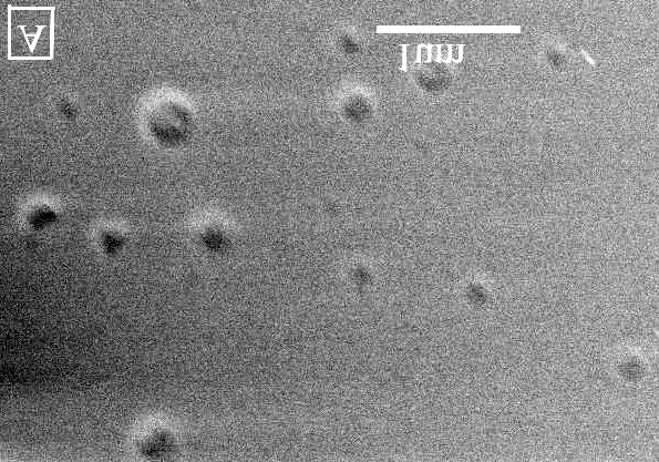
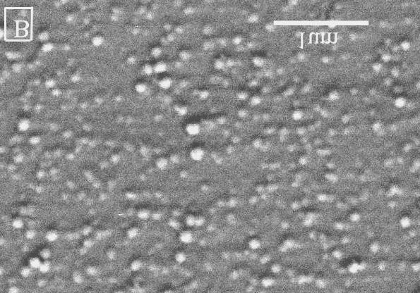
4 was Torr. A RF-sputtering target was also set up in the sample chamber and was used to produce ABN. The field emission properties were measured by the configuration shown in Fig 1. The sample was stick to the sample holder by a carbon disk and the distance between the sample and the electron collector could be changed by the micrometer screw with a precision of 20 micrometers. The base pressure of this system was Torr. The emission current was collected and measured by the ma-meter and na-meter. Both CBN and ABN samples were prepared on n-type Silicon chips and also on silica glasses for UV-Vis absorption measurements. Fig 2 shows the UV-Vis Absorption Spectrum of CBN. The bandwidth is 4.27eV, similar to that of ABN. SAED and XRD result shows the non-crystalline structure of the prepared films. Fig 3a and b show the SEM images of ABN and CBN respectively. In the former only very few blow-ups can be seen while many fluctuations are observed in the SEM images of CBN where the spots are about 100nm. The field emission was measured and the results are shown in Fig 4. Fig 4a and Fig 4b are the log (I-V) curves of ABN and CBN respectively. The emission currents increase from the order of nano-ampere at low voltage and reach milli-ampere at higher voltage. The ABN curve increases sharply while the current for the CBN grows more steadily. The saturated current density of ABN is much lower than the CBN. The ln(i/(v*v)) are calculated and plotted to 1000/V (i.e. F-N Plot as shown in Fig 4c Fig 4d) and straight lines appear in the low electric-field region,indicating the existence of F-N tunneling. Discussions
5 From Fig 4c and Fig 4d, we can find that the F-N tunneling for ABN occurs at 14.4V/μm, while that of CBN begin at 7.14V/μm and reach 1mA at 12.2V/μm (the sample area is about 0.5cm 2 ). The field enhancement factor and the emission area are calculated from F-N plot. β = and α = cm for ABN, whereas β = 381 and α = cm for the CBN. These measurements demonstrate that cluster-deposited BN films has an excellent emission properties. In comparison with atomic-deposition films, cluster films by LECBD have several merits (1) Nano-clusters provide larger band width, which will elevate the energy of the injected electrons from the substrate and benefit tunneling over the surface barrier easily; (2) LECBD gives more emission sites. In the experiments the emission area α = cm of the CBN is two orders higher than that of ABN. Conclusion BN films are prepared by RF-sputtering and LECBD methods and their field emissions were measured. The cluster-deposited BN films show better FE in terms of lower gauge voltage, more emission sites and higher current intensity. It is possible to select the clusters with certain NEA because the cluster sizes could be selected and then nanoclusters of different sizes will have different structures with different electronic band structures. The cluster-deposited BN on n-type Silicon substrate seems a promising substitute for the cascade of Field Emission. Acknowledgement This work was financially supported by the National Natural Science Foundation of China (Grant No , , , , ), the Foundation for University
6 Key Teacher by the Ministry of Education of China (Grant No. GG ), as well as the Analysis and Measurement Foundation of Nanjing University. Our thanks were also extended to Huang Haibo of Southeast University for his help in SEM observation. References 1. C. A. Spindt et al J.Appl.Phys. 47, no 12 (1976) 2. M.J.Powers et al Appl. Phys. Lett. 67,3912 (1995) 3. Chiharu Kihuma et al J. Vac. Sci. Technol. B 19 3 (2001) 4. Y. Yokota S. Tagawa S. T. Sugino Applied Surface Science (1999) 5. G. R. Gu et al. Chin. Phys. Lett X. Z. Ding, X.T. Zeng H. Xie Thin Solid Films H. H. Busta, R.W. Pryor J. Appl. Phys (1997) 8. T. Sugino, C. Kimura, T. Yamamoto, S. Funakawa Diamond and Related Materials Figures Caption 1. The instrument used in FE measurement. The sample is stick to the sample bed by a carbon disk and the distance between the sample and the electron collector can be changed by the micrometer screw with a precision of 20 micrometers. The base pressure of this system is Torr. The emission current is collected and measured by the ma-meter and na-meter, which are protected by resistances of 1KΩ and 1000KΩ respectively. 2. The UV-Vis Absorption Spectrum of CBN. Calculating by Tauc s plot, the bandwidth is 4.27eV.
7 3. SEM images of ABN (a) and CBN (b) respectively. 4. A and B are the log I-V curves of ABN and CBN respectively. Please note that in B the current is given by μa. C and D is F-N plot of ABN and CBN respectively. α and β can be calculated and they are given in the body of the paper. Fig 1
8 Fig 2
9 Fig 3
10 Fig 4
11
Chapter 10. Nanometrology. Oxford University Press All rights reserved.
 Chapter 10 Nanometrology Oxford University Press 2013. All rights reserved. 1 Introduction Nanometrology is the science of measurement at the nanoscale level. Figure illustrates where nanoscale stands
Supporting information:
 Epitaxially Integrating Ferromagnetic Fe 1.3 Ge Nanowire Arrays on Few-Layer Graphene Hana Yoon, Taejoon Kang, Jung Min Lee, Si-in Kim, Kwanyong Seo, Jaemyung Kim, Won Il Park, and Bongsoo Kim,* Department
LECTURE 5 SUMMARY OF KEY IDEAS
 LECTURE 5 SUMMARY OF KEY IDEAS Etching is a processing step following lithography: it transfers a circuit image from the photoresist to materials form which devices are made or to hard masking or sacrificial
Crystalline Surfaces for Laser Metrology
 Crystalline Surfaces for Laser Metrology A.V. Latyshev, Institute of Semiconductor Physics SB RAS, Novosibirsk, Russia Abstract: The number of methodological recommendations has been pronounced to describe
COMPARISON OF J-E CHARACTERISTICS OF A CNT BASED COLD CATHODE GROWN BY CVD AND PECVD
 International Journal of Physics and Research (IJPR) ISSN 2250-0030 Vol.3, Issue 1, Mar 2013, 17-22 TJPRC Pvt. Ltd. COMPARISON OF J-E CHARACTERISTICS OF A CNT BASED COLD CATHODE GROWN BY CVD AND PECVD
CHARACTERIZATION AND FIELD EMISSION PROPERTIES OF FIELDS OF NANOTUBES
 CHARACTERIZATION AND FIELD EMISSION PROPERTIES OF FIELDS OF NANOTUBES Martin MAGÁT a, Jan PEKÁREK, Radimír VRBA a Department of microelectronics, The Faculty of Electrical Engineeering and Communication,
Simulation of the cathode surface damages in a HOPFED during ion bombardment
 Simulation of the cathode surface damages in a HOPFED during ion bombardment Hongping Zhao, Wei Lei, a Xiaobing Zhang, Xiaohua Li, and Qilong Wang Department of Electronic Engineering, Southeast University,
Al/Ti/4H SiC Schottky barrier diodes with inhomogeneous barrier heights
 Al/Ti/4H SiC Schottky barrier diodes with inhomogeneous barrier heights Wang Yue-Hu( ), Zhang Yi-Men( ), Zhang Yu-Ming( ), Song Qing-Wen( ), and Jia Ren-Xu( ) School of Microelectronics and Key Laboratory
SUPPLEMENTARY NOTES Supplementary Note 1: Fabrication of Scanning Thermal Microscopy Probes
 SUPPLEMENTARY NOTES Supplementary Note 1: Fabrication of Scanning Thermal Microscopy Probes Fabrication of the scanning thermal microscopy (SThM) probes is summarized in Supplementary Fig. 1 and proceeds
Zurich Open Repository and Archive. Current-Induced Critical State in NbN Thin-Film Structures
 University of Zurich Zurich Open Repository and Archive Winterthurerstr. 190 CH-8057 Zurich http://www.zora.uzh.ch Year: 2008 Current-Induced Critical State in NbN Thin-Film Structures Il in, K; Siegel,
Effect of Spiral Microwave Antenna Configuration on the Production of Nano-crystalline Film by Chemical Sputtering in ECR Plasma
 THE HARRIS SCIENCE REVIEW OF DOSHISHA UNIVERSITY, VOL. 56, No. 1 April 2015 Effect of Spiral Microwave Antenna Configuration on the Production of Nano-crystalline Film by Chemical Sputtering in ECR Plasma
Chapter 12. Nanometrology. Oxford University Press All rights reserved.
 Chapter 12 Nanometrology Introduction Nanometrology is the science of measurement at the nanoscale level. Figure illustrates where nanoscale stands in relation to a meter and sub divisions of meter. Nanometrology
Recent Status of Polarized Electron Sources at Nagoya University
 Recent Status of Polarized Electron Sources at Nagoya University M. Kuwahara, N. Yamamoto, F. Furuta, T. Nakanishi, S. Okumi, M. Yamamoto, M. Kuriki *, T. Ujihara ** and K. Takeda ** Graduate School of
A HYDROGEN SENSITIVE Pd/GaN SCHOTTKY DIODE SENSOR
 Journal of Physical Science, Vol. 17(2), 161 167, 2006 161 A HYDROGEN SENSITIVE Pd/GaN SCHOTTKY DIODE SENSOR A.Y. Hudeish 1,2* and A. Abdul Aziz 1 1 School of Physics, Universiti Sains Malaysia, 11800
Energy fluxes in plasmas for fabrication of nanostructured materials
 Energy fluxes in plasmas for fabrication of nanostructured materials IEAP, Universität Kiel 2nd Graduate Summer Institute "Complex Plasmas" August 5-13, 2010 in Greifswald (Germany) AG 1 Outline Motivation
1 Corresponding author:
 Scanning Tunneling Microscopy Study of Cr-doped GaN Surface Grown by RF Plasma Molecular Beam Epitaxy Muhammad B. Haider, Rong Yang, Hamad Al-Brithen, Costel Constantin, Arthur R. Smith 1, Gabriel Caruntu
Gaetano L Episcopo. Scanning Electron Microscopy Focus Ion Beam and. Pulsed Plasma Deposition
 Gaetano L Episcopo Scanning Electron Microscopy Focus Ion Beam and Pulsed Plasma Deposition Hystorical background Scientific discoveries 1897: J. Thomson discovers the electron. 1924: L. de Broglie propose
Theoretical Study on Graphene Silicon Heterojunction Solar Cell
 Copyright 2015 American Scientific Publishers All rights reserved Printed in the United States of America Journal of Nanoelectronics and Optoelectronics Vol. 10, 1 5, 2015 Theoretical Study on Graphene
Chapter 103 Spin-Polarized Scanning Tunneling Microscopy
 Chapter 103 Spin-Polarized Scanning Tunneling Microscopy Toyo Kazu Yamada Keywords Spin-polarized tunneling current Spin polarization Magnetism 103.1 Principle Spin-polarized scanning tunneling microscopy
Atomic layer deposition of titanium nitride
 Atomic layer deposition of titanium nitride Jue Yue,version4, 04/26/2015 Introduction Titanium nitride is a hard and metallic material which has found many applications, e.g.as a wear resistant coating[1],
Structures and Field Emission Properties of Silicon Nanowire Arrays Implanted with Energetic Carbon Ion Beam
 Copyright 212 American Scientific Publishers All rights reserved Printed in the United States of America Journal of Nanoscience and Nanotechnology Vol. 12, 1 5, 212 Structures and Field Emission Properties
Large Storage Window in a-sinx/nc-si/a-sinx Sandwiched Structure
 2017 Asia-Pacific Engineering and Technology Conference (APETC 2017) ISBN: 978-1-60595-443-1 Large Storage Window in a-sinx/nc-si/a-sinx Sandwiched Structure Xiang Wang and Chao Song ABSTRACT The a-sin
SUPPLEMENTARY INFORMATION
 In the format provided by the authors and unedited. Intrinsically patterned two-dimensional materials for selective adsorption of molecules and nanoclusters X. Lin 1,, J. C. Lu 1,, Y. Shao 1,, Y. Y. Zhang
Quasi-periodic nanostructures grown by oblique angle deposition
 JOURNAL OF APPLIED PHYSICS VOLUME 94, NUMBER 12 15 DECEMBER 2003 Quasi-periodic nanostructures grown by oblique angle deposition T. Karabacak, a) G.-C. Wang, and T.-M. Lu Department of Physics, Applied
OPTICAL ANALYSIS OF ZnO THIN FILMS USING SPECTROSCOPIC ELLIPSOMETRY AND REFLECTOMETRY.
 OPTICAL ANALYSIS OF ZnO THIN FILMS USING SPECTROSCOPIC ELLIPSOMETRY AND REFLECTOMETRY Katarína Bombarová 1, Juraj Chlpík 1,2, Soňa Flickyngerová 3, Ivan Novotný 3, Július Cirák 1 1 Institute of Nuclear
Effects of Ligand on the Absorbance and Transmittance of Chemical Bath Deposited Zinc Sulphide Thin Film
 Available online at www.pelagiaresearchlibrary.com Advances in Applied Science Research, 2012, 3 (5):2821-2825 ISSN: 0976-8610 CODEN (USA): AASRFC Effects of Ligand on the Absorbance and Transmittance
Infrastructure of Thin Films Laboratory in Institute of Molecular Physics Polish Academy of Sciences
 Infrastructure of Thin Films Laboratory in Institute of Molecular Physics Polish Academy of Sciences Outline Sample preparation Magnetron sputtering Ion-beam sputtering Pulsed laser deposition Electron-beam
ON ELECTRON FIELD EMISSION FROM NANOCARBONS
 ON ELECTRON FIELD EMISSION FROM NANOCARBONS Igor S. Altman, Peter V. Pikhitsa, Mansoo Choi National CRI Center for Nano Particle Control, Institute of Advanced Machinery and Design, School of Mechanical
Electronic Supplementary Information: Synthesis and Characterization of Photoelectrochemical and Photovoltaic Cu2BaSnS4 Thin Films and Solar Cells
 Electronic Supplementary Material (ESI) for Journal of Materials Chemistry C. This journal is The Royal Society of Chemistry 2017 Electronic Supplementary Information: Synthesis and Characterization of
Nanostructure. Materials Growth Characterization Fabrication. More see Waser, chapter 2
 Nanostructure Materials Growth Characterization Fabrication More see Waser, chapter 2 Materials growth - deposition deposition gas solid Physical Vapor Deposition Chemical Vapor Deposition Physical Vapor
MICROCHIP MANUFACTURING by S. Wolf
 by S. Wolf Chapter 15 ALUMINUM THIN-FILMS and SPUTTER-DEPOSITION 2004 by LATTICE PRESS CHAPTER 15 - CONTENTS Aluminum Thin-Films Sputter-Deposition Process Steps Physics of Sputter-Deposition Magnetron-Sputtering
Depth Distribution Functions of Secondary Electron Production and Emission
 Depth Distribution Functions of Secondary Electron Production and Emission Z.J. Ding*, Y.G. Li, R.G. Zeng, S.F. Mao, P. Zhang and Z.M. Zhang Hefei National Laboratory for Physical Sciences at Microscale
Onset of the Meissner effect at 65 K in FeSe thin film grown on Nb doped SrTiO 3 substrate
 Onset of the Meissner effect at 65 K in FeSe thin film grown on Nb doped SrTiO 3 substrate Zuocheng Zhang 1,4*, Yihua Wang 2,3*, Qi Song 2,5*, Chang Liu 1,4, Rui Peng 2,5, K.A. Moler 3, Donglai Feng 2,5
NUCLEAR TRANSMUTATION IN DEUTERED PD FILMS IRRADIATED BY AN UV LASER
 Castellano, et al. Nuclear Transmutation in Deutered Pd Films Irradiated by an UV Laser. in 8th International Conference on Cold Fusion. 2000. Lerici (La Spezia), Italy: Italian Physical Society, Bologna,
Scanning Tunneling Microscopy
 Scanning Tunneling Microscopy Scanning Direction References: Classical Tunneling Quantum Mechanics Tunneling current Tunneling current I t I t (V/d)exp(-Aφ 1/2 d) A = 1.025 (ev) -1/2 Å -1 I t = 10 pa~10na
A novel sputtering technique: Inductively Coupled Impulse Sputtering (ICIS)
") IOP Conference Series: Materials Science and Engineering A novel sputtering technique: Inductively Coupled Impulse Sputtering (ICIS) To cite this article: D A L Loch and A P Ehiasarian 2012 IOP Conf. Ser.:
IOP Conference Series: Materials Science and Engineering A novel sputtering technique: Inductively Coupled Impulse Sputtering (ICIS) To cite this article: D A L Loch and A P Ehiasarian 2012 IOP Conf. Ser.:
Scaling during shadowing growth of isolated nanocolumns
 Scaling during shadowing growth of isolated nanocolumns T. Karabacak, J. P. Singh, Y.-P. Zhao, G.-C. Wang, and T.-M. Lu Department of Physics, Applied Physics and Astronomy, Rensselaer Polytechnic Institute,
Perovskite Solar Cells Powered Electrochromic Batteries for Smart. Windows
 Electronic Supplementary Material (ESI) for Materials Horizons. This journal is The Royal Society of Chemistry 2016 Supporting Information for Perovskite Solar Cells Powered Electrochromic Batteries for
Nanochannel-Assisted Perovskite Nanowires: Growth Mechanisms. to Photodetector Applications
 Supplementary Information: Nanochannel-Assisted Perovskite Nanowires: Growth Mechanisms to Photodetector Applications Qitao Zhou, Jun Gyu Park, Riming Nie, Ashish Kumar Thokchom, Dogyeong Ha, Jing Pan,
Surface Defects on Natural MoS 2
 Supporting Information: Surface Defects on Natural MoS 2 Rafik Addou 1*, Luigi Colombo 2, and Robert M. Wallace 1* 1 Department of Materials Science and Engineering, The University of Texas at Dallas,
Off-axis unbalanced magnetron sputtering of YBa2Cu307 thin films
 ELSEVIER Materials Chemistry and Physics 49 (1997) 229-233 MATERIALS CHEMISTRYAND PHYSICS Off-axis unbalanced magnetron sputtering of YBa2Cu307 thin films Wen-Chou Tsai, Tseung-Yuen Tseng * Institute of
Effect of nitrogen addition on the band gap, core level shift, surface energy, and the threshold field of electron emission of the SrTiO 3 thin films
 JOURNAL OF APPLIED PHYSICS 102, 114906 2007 Effect of nitrogen addition on the band gap, core level shift, surface energy, and the threshold field of electron emission of the SrTiO 3 thin films H. J. Bian
Supplementary Figure S1. AFM images of GraNRs grown with standard growth process. Each of these pictures show GraNRs prepared independently,
 Supplementary Figure S1. AFM images of GraNRs grown with standard growth process. Each of these pictures show GraNRs prepared independently, suggesting that the results is reproducible. Supplementary Figure
Enhancing Perovskite Solar Cell Performance by Interface Engineering Using CH 3 NH 3 PbBr 0.9 I 2.1 Quantum Dots
 Supporting Information for Enhancing Perovskite Solar Cell Performance by Interface Engineering Using CH 3 NH 3 PbBr 0.9 I 2.1 Quantum Dots Mingyang Cha,, Peimei Da,, Jun Wang, Weiyi Wang, Zhanghai Chen,
Improving the field-emission properties of carbon nanotubes by magnetically controlled nickel-electroplating treatment
 Improving the field-emission properties of carbon nanotubes by magnetically controlled nickel-electroplating treatment Zheng Long-Wu( ), Hu Li-Qin( ), Xiao Xiao-Jing( ), Yang Fan( ), Lin He( ), and Guo
DEPOSITION OF THIN TiO 2 FILMS BY DC MAGNETRON SPUTTERING METHOD
 Chapter 4 DEPOSITION OF THIN TiO 2 FILMS BY DC MAGNETRON SPUTTERING METHOD 4.1 INTRODUCTION Sputter deposition process is another old technique being used in modern semiconductor industries. Sputtering
Supplementary Figure 1 Detailed illustration on the fabrication process of templatestripped
 Supplementary Figure 1 Detailed illustration on the fabrication process of templatestripped gold substrate. (a) Spin coating of hydrogen silsesquioxane (HSQ) resist onto the silicon substrate with a thickness
Electroluminescence from Silicon and Germanium Nanostructures
 Electroluminescence from silicon Silicon Getnet M. and Ghoshal S.K 35 ORIGINAL ARTICLE Electroluminescence from Silicon and Germanium Nanostructures Getnet Melese* and Ghoshal S. K.** Abstract Silicon
Electronic Supplementary Information
 Electronic Supplementary Material (ESI) for ChemComm. This journal is The Royal Society of Chemistry 2018 Electronic Supplementary Information Room-Temperature Film Formation of Metal Halide Perovskites
Plasmonic Hot Hole Generation by Interband Transition in Gold-Polyaniline
 Supplementary Information Plasmonic Hot Hole Generation by Interband Transition in Gold-Polyaniline Tapan Barman, Amreen A. Hussain, Bikash Sharma, Arup R. Pal* Plasma Nanotech Lab, Physical Sciences Division,
HEMS Low Power Carbon Nanotube Field Emission Electron Source for Chemical Ionization Mass Spectrometry
 Low Power Carbon Nanotube Field Emission Electron Source for Chemical Ionization Mass Spectrometry HEMS 2015 Charles B. Parker, Erich J. Radauscher, Adam D. Keil, Mitch Wells, Jason J. Amsden, Jeffrey
Superconducting Single-photon Detectors
 : Quantum Cryptography Superconducting Single-photon Detectors Hiroyuki Shibata Abstract This article describes the fabrication and properties of a single-photon detector made of a superconducting NbN
Influence of Size on the Properties of Materials
 Influence of Size on the Properties of Materials M. J. O Shea Kansas State University mjoshea@phys.ksu.edu If you cannot get the papers connected to this work, please e-mail me for a copy 1. General Introduction
CARBON NANOSTRUCTURES SYNTHESIZED THROUGH GRAPHITE ETCHING
 CARBON NANOSTRUCTURES SYNTHESIZED THROUGH GRAPHITE ETCHING Q. Yang 1, C. Xiao 1, R. Sammynaiken 2 and A. Hirose 1 1 Plasma Physics Laboratory, University of Saskatchewan, 116 Science Place Saskatoon, SK
ToF-SIMS or XPS? Xinqi Chen Keck-II
 ToF-SIMS or XPS? Xinqi Chen Keck-II 1 Time of Flight Secondary Ion Mass Spectrometry (ToF-SIMS) Not ToF MS (laser, solution) X-ray Photoelectron Spectroscopy (XPS) 2 3 Modes of SIMS 4 Secondary Ion Sputtering
Nano-ECRIS project: a new ECR ion source at Toyo University to produce endohedral fullerenes
 The Bio-Nano Nano-ECRIS project: a new ECR ion source at Toyo University to produce endohedral fullerenes ECRIS 2008 18th International Workshop on ECR Ion Sources Chicago, Illinois USA - September 15-18,
Investigation of H 2 :CH 4 Plasma Composition by Means of Spatially Resolved Optical Spectroscopy
 Vol. 114 (2008) ACTA PHYSICA POLONICA A No. 6 A Optical and Acoustical Methods in Science and Technology Investigation of H 2 :CH 4 Plasma Composition by Means of Spatially Resolved Optical Spectroscopy
Enhancing the Performance of Organic Thin-Film Transistor using a Buffer Layer
 Proceedings of the 9th International Conference on Properties and Applications of Dielectric Materials July 19-23, 29, Harbin, China L-7 Enhancing the Performance of Organic Thin-Film Transistor using
IN THE NAME OF ALLAH, THE MOST MERCIFUL AND COMPASSIONATE
 IN THE NAME OF ALLAH, THE MOST MERCIFUL AND COMPASSIONATE Ion Beam Analysis of Diamond Thin Films Sobia Allah Rakha Experimental Physics Labs 04-03-2010 Outline Diamond Nanostructures Deposition of Diamond
Supplementary Information
 Supplementary Information Chemical and Bandgap Engineering in Monolayer Hexagonal Boron Nitride Kun Ba 1,, Wei Jiang 1,,Jingxin Cheng 2, Jingxian Bao 1, Ningning Xuan 1,Yangye Sun 1, Bing Liu 1, Aozhen
Flexible Asymmetrical Solid-state Supercapacitors Based on Laboratory Filter Paper
 SUPPORTING INFORMATION Flexible Asymmetrical Solid-state Supercapacitors Based on Laboratory Filter Paper Leicong Zhang,,,# Pengli Zhu,,,#, * Fengrui Zhou, Wenjin Zeng, Haibo Su, Gang Li, Jihua Gao, Rong
Effects of plasma treatment on the precipitation of fluorine-doped silicon oxide
 ARTICLE IN PRESS Journal of Physics and Chemistry of Solids 69 (2008) 555 560 www.elsevier.com/locate/jpcs Effects of plasma treatment on the precipitation of fluorine-doped silicon oxide Jun Wu a,, Ying-Lang
Nova 600 NanoLab Dual beam Focused Ion Beam IITKanpur
 Nova 600 NanoLab Dual beam Focused Ion Beam system @ IITKanpur Dual Beam Nova 600 Nano Lab From FEI company (Dual Beam = SEM + FIB) SEM: The Electron Beam for SEM Field Emission Electron Gun Energy : 500
2 Title: "Ultrathin flexible electronic device based on tunneling effect: a flexible ferroelectric tunnel
 Electronic Supplementary Material (ESI) for Journal of Materials Chemistry C. This journal is The Royal Society of Chemistry 208 Supplementary information 2 Title: "Ultrathin flexible electronic device
SUPPLEMENTARY INFORMATION
 DOI: 10.1038/NCHEM.2491 Experimental Realization of Two-dimensional Boron Sheets Baojie Feng 1, Jin Zhang 1, Qing Zhong 1, Wenbin Li 1, Shuai Li 1, Hui Li 1, Peng Cheng 1, Sheng Meng 1,2, Lan Chen 1 and
ABSTRACT 1. INTRODUCTION 2. EXPERIMENT
 Fabrication of Nanostructured Heterojunction LEDs Using Self-Forming Moth-Eye Type Arrays of n-zno Nanocones Grown on p-si (111) Substrates by Pulsed Laser Deposition D. J. Rogers 1, V. E. Sandana 1,2,3,
Scanning Tunneling Microscopy Studies of the Ge(111) Surface
 Surface") VC Scanning Tunneling Microscopy Studies of the Ge(111) Surface Anna Rosen University of California, Berkeley Advisor: Dr. Shirley Chiang University of California, Davis August 24, 2007 Abstract: This
VC Scanning Tunneling Microscopy Studies of the Ge(111) Surface Anna Rosen University of California, Berkeley Advisor: Dr. Shirley Chiang University of California, Davis August 24, 2007 Abstract: This
Physics and Material Science of Semiconductor Nanostructures
 Physics and Material Science of Semiconductor Nanostructures PHYS 570P Prof. Oana Malis Email: omalis@purdue.edu Course website: http://www.physics.purdue.edu/academic_programs/courses/phys570p/ 1 Course
Plasma Diagnosis for Microwave ECR Plasma Enhanced Sputtering Deposition of DLC Films
 Plasma Science and Technology, Vol.14, No.2, Feb. 2012 Plasma Diagnosis for Microwave ECR Plasma Enhanced Sputtering Deposition of DLC Films PANG Jianhua ( ) 1, LU Wenqi ( ) 1, XIN Yu ( ) 2, WANG Hanghang
Laser-induced treatment of silicon in air and formation of Si/SiO x photoluminescent nanostructured layers
 Materials Science and Engineering B101 (2003) 60/64 www.elsevier.com/locate/mseb Laser-induced treatment of silicon in air and formation of Si/SiO x photoluminescent nanostructured layers A.V. Kabashin
Supplementary Information
 Electronic Supplementary Material (ESI) for Nanoscale. This journal is The Royal Society of Chemistry 2014 Supplementary Information Large-scale lithography-free metasurface with spectrally tunable super
Nanocrystalline Si formation inside SiN x nanostructures usingionized N 2 gas bombardment
 연구논문 한국진공학회지제 16 권 6 호, 2007 년 11 월, pp.474~478 Nanocrystalline Si formation inside SiN x nanostructures usingionized N 2 gas bombardment Min-Cherl Jung 1, Young Ju Park 2, Hyun-Joon Shin 1, Jun Seok Byun
Electronic Supplementary Information for
 Electronic Supplementary Material (ESI) for Journal of Materials Chemistry C. This journal is The Royal Society of Chemistry 018 Electronic Supplementary Information for Broadband Photoresponse Based on
Supporting Information
 Electronic Supplementary Material (ESI) for ChemComm. This journal is The Royal Society of Chemistry 2018 Supporting Information In situ and real-time ToF-SIMS analysis of light-induced chemical changes
TMT4320 Nanomaterials November 10 th, Thin films by physical/chemical methods (From chapter 24 and 25)
") 1 TMT4320 Nanomaterials November 10 th, 2015 Thin films by physical/chemical methods (From chapter 24 and 25) 2 Thin films by physical/chemical methods Vapor-phase growth (compared to liquid-phase growth)
1 TMT4320 Nanomaterials November 10 th, 2015 Thin films by physical/chemical methods (From chapter 24 and 25) 2 Thin films by physical/chemical methods Vapor-phase growth (compared to liquid-phase growth)
Mechanisms of Visible Photoluminescence from Size-Controlled Silicon Nanoparticles
 Mat. Res. Soc. Symp. Proc. Vol. 737 23 Materials Research Society F1.5.1 Mechanisms of Visible Photoluminescence from Size-Controlled Silicon Nanoparticles Toshiharu Makino *, Nobuyasu Suzuki, Yuka Yamada,
Supplementary Figures
 Supplementary Figures Supplementary Figure 1 Thickness calibration of PVDF layers using atomic force microscopy. (a-d) Tapping AFM images of 1 L, 2 Ls, 4 Ls and 20 Ls PVDF films, respectively on Au-coated
Repetition: Physical Deposition Processes
 Repetition: Physical Deposition Processes PVD (Physical Vapour Deposition) Evaporation Sputtering Diode-system Triode-system Magnetron-system ("balanced/unbalanced") Ion beam-system Ionplating DC-glow-discharge
CHARACTERIZATION of NANOMATERIALS KHP
 CHARACTERIZATION of NANOMATERIALS Overview of the most common nanocharacterization techniques MAIN CHARACTERIZATION TECHNIQUES: 1.Transmission Electron Microscope (TEM) 2. Scanning Electron Microscope
Temperature Dependent Current-voltage Characteristics of P- type Crystalline Silicon Solar Cells Fabricated Using Screenprinting
 Temperature Dependent Current-voltage Characteristics of P- type Crystalline Silicon Solar Cells Fabricated Using Screenprinting Process Hyun-Jin Song, Won-Ki Lee, Chel-Jong Choi* School of Semiconductor
Interaction Mechanism of a Field Emission Based THz Oscillator
 PIERS ONLINE, VOL. 3, NO. 7, 2007 1011 Interaction Mechanism of a Field Emission Based THz Oscillator M. C. Lin 1 and P. S. Lu 1, 2 1 NanoScience Simulation Laboratory, Department of Physics, Fu Jen Catholic
M.J. CONDENSED MATTER VOLUME 4, NUMBER 1 1 DECEMBER 2001
 M.J. CONDENSED MATTER VOLUME 4, NUMBER 1 1 DECEMBER 21 Au/n-Si(1) contact homogeneity studied by direct and reverse ballistic electron emission microscopy and spectroscopy A. Chahboun and I. Zorkani L.
Half-Integer Quantum Conductance States
 Supporting Information A 50 mv Cu/SiO /W Memristor with Half-Integer Quantum Conductance States S. R. Nandakumar, Marie Minvielle, Saurabh Nagar, Catherine Dubourdieu, and Bipin Rajendran, Department of
Field emission vacuum power switch using vertically aligned carbon nanotubes
 Field emission vacuum power switch using vertically aligned carbon nanotubes N. L. Rupesinghe, a) M. Chhowalla, K. B. K. Teo, and G. A. J. Amaratunga Department of Engineering, University of Cambridge,
MSE 321 Structural Characterization
 Auger Spectroscopy Auger Electron Spectroscopy (AES) Scanning Auger Microscopy (SAM) Incident Electron Ejected Electron Auger Electron Initial State Intermediate State Final State Physical Electronics
High-Current Y-Ba-Cu-O Coated Conductor using Metal Organic Chemical-Vapor Deposition and Ion-Beam-Assisted Deposition
 SP-T-152 High-Current Y-Ba-Cu-O Coated Conductor using Metal Organic Chemical-Vapor Deposition and Ion-Beam-Assisted Deposition V. Selvamanickam, G. Carota, M. Funk, N. Vo, and P. Haldar U. Balachandran,
Combinatorial RF Magnetron Sputtering for Rapid Materials Discovery: Methodology and Applications
 Combinatorial RF Magnetron Sputtering for Rapid Materials Discovery: Methodology and Applications Philip D. Rack,, Jason D. Fowlkes,, and Yuepeng Deng Department of Materials Science and Engineering University
Secondary Ion Mass Spectrometry (SIMS) Thomas Sky
 Thomas Sky") 1 Secondary Ion Mass Spectrometry (SIMS) Thomas Sky Depth (µm) 2 Characterization of solar cells 0,0 1E16 1E17 1E18 1E19 1E20 0,2 0,4 0,6 0,8 1,0 1,2 P Concentration (cm -3 ) Characterization Optimization
1 Secondary Ion Mass Spectrometry (SIMS) Thomas Sky Depth (µm) 2 Characterization of solar cells 0,0 1E16 1E17 1E18 1E19 1E20 0,2 0,4 0,6 0,8 1,0 1,2 P Concentration (cm -3 ) Characterization Optimization
Investigation of tungsten incorporated amorphous carbon lm
 Thin Solid Films 355±356 (1999) 174±178 www.elsevier.com/locate/tsf Investigation of tungsten incorporated amorphous carbon lm Rusli a, *, S.F. Yoon a, H. Yang a, J. Ahn a, Q.F. Huang a, Q. Zhang a, Y.P.
Metallic: 2n 1. +n 2. =3q Armchair structure always metallic = 2
 Properties of CNT d = 2.46 n 2 2 1 + n1n2 + n2 2π Metallic: 2n 1 +n 2 =3q Armchair structure always metallic a) Graphite Valence(π) and Conduction(π*) states touch at six points(fermi points) Carbon Nanotube:
High-temperature single-electron transistor based on a gold nanoparticle
 High-temperature single-electron transistor based on a gold nanoparticle SA Dagesyan 1 *, A S Stepanov 2, E S Soldatov 1, G Zharik 1 1 Lomonosov Moscow State University, faculty of physics, Moscow, Russia,
Nanotechnology Fabrication Methods.
 Nanotechnology Fabrication Methods. 10 / 05 / 2016 1 Summary: 1.Introduction to Nanotechnology:...3 2.Nanotechnology Fabrication Methods:...5 2.1.Top-down Methods:...7 2.2.Bottom-up Methods:...16 3.Conclusions:...19
STUDY OF LAYERS OF METAL NANOPARTICLES ON SEMICONDUCTOR WAFERS FOR HYDROGEN DETECTION
 STUDY OF LAYERS OF METAL NANOPARTICLES ON SEMICONDUCTOR WAFERS FOR HYDROGEN DETECTION Martin MULLER a, b, Karel ZDANSKY a, Jiri ZAVADIL a, Katerina PIKSOVA b a INSTITUTE OF PHOTONICS AND ELECTRONICS, CZECH
High-current-density field emitters based on arrays of carbon nanotube bundles
 High-current-density field emitters based on arrays of carbon nanotube bundles Harish M. Manohara, Michael J. Bronikowski, a) Michael Hoenk, Brian D. Hunt, and Peter H. Siegel Jet Propulsion Laboratory,
This document is downloaded from DR-NTU, Nanyang Technological University Library, Singapore.
 This document is downloaded from DR-NTU, Nanyang Technological University Library, Singapore. Title Author(s) Citation Fiber-optic temperature sensor based on temperaturedependent refractive index of Germanium-silica
Radiative Heat Transfer at the Nanoscale. Pramod Reddy University of Michigan, Ann Arbor
 Radiative Heat Transfer at the Nanoscale 40µm Pramod Reddy University of Michigan, Ann Arbor Acknowledgements Edgar Meyhofer Juan Carlos Cuevas Francisco Garcia Vidal B. Song K. Kim V. Fernandez J. Fiest
Supplementary Figure S1. AFM characterizations and topographical defects of h- BN films on silica substrates. (a) (c) show the AFM height
 (c) show the AFM height") Supplementary Figure S1. AFM characterizations and topographical defects of h- BN films on silica substrates. (a) (c) show the AFM height topographies of h-bn film in a size of ~1.5µm 1.5µm, 30µm 30µm
Supplementary Figure S1. AFM characterizations and topographical defects of h- BN films on silica substrates. (a) (c) show the AFM height topographies of h-bn film in a size of ~1.5µm 1.5µm, 30µm 30µm
Abnormal PL spectrum in InGaN MQW surface emitting cavity
 Abnormal PL spectrum in InGaN MQW surface emitting cavity J. T. Chu a, Y.-J. Cheng b, H. C. Kuo a, T. C. Lu a, and S. C. Wang a a Department of Photonics & Institute of Electro-Optical Engineering, National
The effect of the chamber wall on fluorocarbonassisted atomic layer etching of SiO 2 using cyclic Ar/C 4 F 8 plasma
 The effect of the chamber wall on fluorocarbonassisted atomic layer etching of SiO 2 using cyclic Ar/C 4 F 8 plasma Running title: The effect of the chamber wall on FC assisted atomic layer etching of
Real-time and in-line Optical monitoring of Functional Nano-Layer Deposition on Flexible Polymeric Substrates
 Real-time and in-line Optical monitoring of Functional Nano-Layer Deposition on Flexible Polymeric Substrates S. Logothetidis Lab for Thin Films, Nanosystems & Nanometrology, Aristotle University of Thessaloniki,