CHARGE TRANSPORT ALONG MOLECULAR WIRES
|
|
|
- Joshua Walters
- 5 years ago
- Views:
Transcription
1 CHARGE TRANSPORT ALONG MOLECULAR WIRES Aleksey Kocherzhenko DelftChemTech Faculty Colloquium / March 9, 2009 DelftChemTech: THREADMILL:


2 The Long Way to a Conventional Computer

3 2 (which could be even longer)
4 3 and the Self-Assembling Molecular Computer

5 Defects? No problem! 4 J. R. Heath, et al. Science, 280, 1716 (1998)
6 Molecular wires are interesting: electronics, in it s quest for higher integration densities, is approaching molecular dimensions; bottom-up approaches open up new opportunities for creating self-assembling nanoelectronic devices; there is a possibility to tune the conductivity and other properties of molecules to desired specifications; processing polymers is cheaper than processing inorganic semiconductors. Why molecular wires, not small molecules? Also those! 5
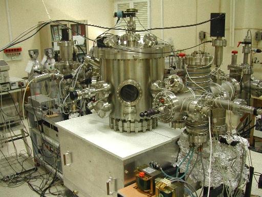
7 Conductivity characterization techniques Contact techniques: molecules between electrodes, electrode and STM tip, etc. Drawback: measured conductivity / charge carrier mobility is to a large extent determined by contacts. Contactless techniques are required to study intramolecular charge transport. 6
: a contactless")


8 Pulse radiolysis time-resolved microwave conductivity (PR-TRMC): a contactless technique Close to uniform concentration of Bz + and e - produced in O 2 saturated benzene solution of polymer (P n ) Creation of charge carriers by pulse radiolysis (2 50 ns pulse of 3 MeV electrons) Detection by TRMC Microwaves are absorbed by mobile charge carriers ΔP P = AΔσ 7
9 TRMC experimental results O 2 -saturated solution of polymers (P) in benzene (Bz) 1 3 Irradiated with short (10 ns) pulse of 3 MeV electrons (e - ) Close to uniform concentration of Bz + and e - 2 T R 1 2 O 2 + e = O 2 Bz + + P = Bz + P + M C 3 P + + O 2 = P + O 2 Mobility independent of the chain length 8
10 Conducting polymers: Ladder-type PPP µ h ~ 600 cm 2 V 1 s 1 ( Silicon : µ Si h 450 cm 2 V 1 s 1 ) µ = v dr E ; σ = enµ 9 P. Prins, et al. Phys. Rev. Lett., 96, (2006)
11 Conducting polymers: Zn-porphyrin wires µ h 0.1 cm 2 V 1 s 1 Is the difference in the mobility only quantitative, or also qualitative? 10 F. C. Grozema, et al. JACS, 129, (2007)
12 Possible charge transport mechanisms Two extreme cases: Band-like transport typically occurs for systems with: - delocalized charges; - high charge carrier mobilities; - large electronic couplings. Hopping transport typically occurs for systems with: - localized charges; - lower charge carrier mobilities; - smaller electronic couplings. It is not always easy to distinguish between the above two mechanisms. In real systems a mixture of the two often occurs. 11 F. C. Grozema; Siebbeles, L. D. A. Int. Rev. Phys. Chem. 27, 87 (2008)
13 Why is the mechanism of charge transport important? Polymers with different mechanisms of charge transport will not only show very different charge carrier mobilities, but also a very different dependence of the mobility on various parameters: polymer chain length, temperature, external electric field frequency, 12
14 Relative stability Thermodynamic parameter: is it energetically favorable for the charge to localize on one unit or to delocalize over many? 100% 0% or 50% 50% (with corresponding geometries) +1, delocalized ( ) 0.5Oxidized Δ = E 0.5Oxidized ( ) +1, localized ( ) Neutral E Oxidized ( ) 13
15 Charge transport simulations Polymers consist of a very large number of atoms ab initio quantum-chemical calculations require a lot of time (calculation time N 4, N - number of atoms) To reduce calculation time, we can split the problem into two steps: calculate parameters of repeat units (same for all identical repeat units) and interconnects between them (same for all pairs of adjacent repeat units) calculate transport along the polymer chain in terms of the calculated parameters (neglecting the details of charge transport within a repeat unit) 14
16 The model i = 1,10 ε 1 ε 3i 1 ε 3i J 3i 1, 3i J 3i, 3i+1 Saturated hydrocarbon chains ε 32 ε 33 ε 34 Molecular site (Type 1) ε 3i+1 Molecular site (Type 2) Approximation: molecular sites have no internal structure 15
 t = HΨ( t) Classically propagate geometry (relevant coordinates) J( θ) = J( 0)cosθ θ( t + Δt) = θ( t) 1 2τ rot k B T ' ( V tor θ ) * Δt ± Δt τ rot 16 P. Prins, et al. Mol. Simulations.")
17 Band-like transport simulation Simultaneously: Quantum-mechanically propagate charge on polymer chain # ε 1 J 1,2 0 0 & % J 1,2 ε 2 J 2,3 0 ( % ( H = % 0 J 2,3 ε 3 0 ( % ( % ( $ % ε 34 '( i Ψ( t) t = HΨ( t) Classically propagate geometry (relevant coordinates) J( θ) = J( 0)cosθ θ( t + Δt) = θ( t) 1 2τ rot k B T ' ( V tor θ ) * Δt ± Δt τ rot 16 P. Prins, et al. Mol. Simulations. 32, 695 (2006)
18 Band-like transport simulation algorithm Sample θ(t = 0) from Boltzman distribution Not yet N times Δx 2 ( t) H = ε i a i + a i + J i,j i Ψ( t) eq ( ) = Φ where n0 ε i ( t) = ε ph,fl + Δε fluct ( t) = HΨ( t) t J i, j ( t) = Acos[ θ( t) Ψ( t) ] Ψ 0 P(θ) = [ ( ) k B T] ( ) k B T exp V tor θ [ ] exp V tor θ dθ i i j a i + a j N times V tor (θ) (mev) θ θ (degrees) Average over N values of Δx 2 (t) θ( t + Δt) = θ( t) µ 1D ( ω) = eω 2 2k B T µ 1D DC 1 2τ rot k B T ( ) Δx 2 t = ed k B T, ' ( V tor θ ( ) where ) * Δt ± Δt τ rot cos( ω t)d t D = Δx2 ( t) 2t 17
19 The charge transport mechanism in ladder-type PPP is band-like µ h ~ 600 cm 2 V 1 s 1 18
20 Hopping transport The charge can be described classically 19
21 Hopping transport simulation Marcus hopping rate: Γ ij = 2π J ij 2 1 ( ) 2 & 4πλk B T exp E E + λ j i ( 4λk B T ' ( ) + * + Γ i, i 1 Γ i, i+1 E i 2 E i 1 E i E i+1 E i+2 Δx 2 ( t) µ 1D ( ω) 20 Parameters: E i J ij λ equilibrium energy of charge localization site i electronic coupling between sites i and j reorganization energy, characterizes distortion of the molecular geometry when a charge is placed on a site
22 The charge transport mechanism in Zn-porphyrin based wires is hopping µ h 0.1 cm 2 V 1 s 1 21
23 22 Hopping transport mobility is extremely sensitive to disorder in the polymer and in its environment
24 Disorder can be engineered Ladder-like double strand structures formed upon addition of bidentate ligand (Bipy=4,4 -bipyridyl) to benzene solution. 23
25 Experimental results: ladder-like structure without Bipy with Bipy µ = cm 2 /(V s) µ = 0.93 cm 2 /(V s) 24
26 Conclusions Molecular electronics is feasible Conjugated polymers are promising and versatile materials for electronic applications Charge transfer properties of conjugated polymers can be controlled supramolecularly: - either by just changing their molecular conformation (changing solvent, preparing aligned films) - or by changing the disorder in their environment 25

27 Acknowledgements University of Oxford: - Prof. Dr. Harry Anderson - Dr. Shane MacDonnell - Dr. Coralie Houarner-Rassin - Giuseppe Sforazzini - Johannes Sprafke University of Mons Hainaut: - Prof. Dr. David Beljonne - Michael Wykes Belarusian State University: - Prof. Dr. Nikolai A. Poklonski Delft University of Technology: - Dr. Paulette Prins - Sameer Patwardhan Funding: - European Union 26
28 THANK YOU FOR YOUR ATTENTION! CHARGE TRANSPORT ALONG MOLECULAR WIRES Aleksey Kocherzhenko DelftChemTech: THREADMILL: Delft University of Technology, Faculty of Applied Sciences DelftChemTech, Opto-electronic Materials Section Julianalaan 136, 2628 BL, Delft, The Netherlands
The Study of Charge Carrier Transports in the Calamitic Liquid Crystals 5, 5 -di-(decyl-pyridin-yl) - 2 Bithiophene.
 - 2 Bithiophene.") The Study of Charge Carrier Transports in the Calamitic Liquid Crystals 5, 5 -di-(decyl-pyridin-yl) - 2 Bithiophene Naresh Shakya * C. Pokhrel* and B. Ellman* Y. Getmanenko** and R. J. Twieg** *Department
The Study of Charge Carrier Transports in the Calamitic Liquid Crystals 5, 5 -di-(decyl-pyridin-yl) - 2 Bithiophene Naresh Shakya * C. Pokhrel* and B. Ellman* Y. Getmanenko** and R. J. Twieg** *Department
Triplet state diffusion in organometallic and organic semiconductors
 Triplet state diffusion in organometallic and organic semiconductors Prof. Anna Köhler Experimental Physik II University of Bayreuth Germany From materials properties To device applications Organic semiconductors
Anirban Som
 Anirban Som 01-11-14 Introduction Supramolecular chemistry generates complex structures over a range of length scales. Structures such as DNA origami, supramolecular polymers etc. are formed via multiple
Brownian dynamics simulations of charge mobility on. conjugated polymers in solution
 1 Brownian dynamics simulations of charge mobility on conjugated polymers in solution Nicolae M. Albu and David J. Yaron Department of Chemistry, Carnegie Mellon University, Pittsburgh, PA 15213 Keywords:
Bottom-up modelling of charge transport in organic semiconductors
 Bottom-up modelling of charge transport in organic semiconductors David L. Cheung Department of Chemistry & Centre for Scientific Computing University of Warwick LCOPV 2010 Boulder 7th-10th August 2010
Semiconductor Polymer
 Semiconductor Polymer Organic Semiconductor for Flexible Electronics Introduction: An organic semiconductor is an organic compound that possesses similar properties to inorganic semiconductors with hole
From exhaustive simulations to key principles in DNA nanoelectronics
 From exhaustive simulations to key principles in DNA nanoelectronics Dvira Segal Department of Chemistry University of Toronto Roman Korol (undergrad) Hyehwang Kim (undergrad) Michael Kilgour (grad) Challenge:
Theoretical Study of Electric Field-Dependent Polaron-type Mobility in Conjugated Polymers. Helena M. G. Correia, Marta M. D.
 Theoretical Study of Electric Field-Dependent Polaron-type Mobility in Conjugated Polymers Helena M. G. Correia, Marta M. D. Ramos Physics Department, University of Minho, Campus de Gualtar, 4710-059 Braga,
Nanoelectronics. Topics
 Nanoelectronics Topics Moore s Law Inorganic nanoelectronic devices Resonant tunneling Quantum dots Single electron transistors Motivation for molecular electronics The review article Overview of Nanoelectronic
Supplementary Figure 1. Crystal packing of pentacene.
 t 3 t 4 t 1 t 2 Supplementary Figure 1. Crystal packing of pentacene. The largestholecharge transfer integrals are shown in red:t 1 = 75 mev, t 2 = 32 mev, t 3 = 20 mev, t 4 = 6 mev. Note that IRactive
Directions for simulation of beyond-cmos devices. Dmitri Nikonov, George Bourianoff, Mark Stettler
 Directions for simulation of beyond-cmos devices Dmitri Nikonov, George Bourianoff, Mark Stettler Outline Challenges and responses in nanoelectronic simulation Limits for electronic devices and motivation
Winter College on Optics and Energy February Photophysics for photovoltaics. G. Lanzani CNST of Milano Italy
 13-4 Winter College on Optics and Energy 8-19 February 010 Photophysics for photovoltaics G. Lanzani CNST of IIT@POLIMI Milano Italy Winter College on Optics and Energy Guglielmo Lanzani CNST of IIT@POLIMI,
6.5 mm. ε = 1%, r = 9.4 mm. ε = 3%, r = 3.1 mm
 Supplementary Information Supplementary Figures Gold wires Substrate Compression holder 6.5 mm Supplementary Figure 1 Picture of the compression holder. 6.5 mm ε = 0% ε = 1%, r = 9.4 mm ε = 2%, r = 4.7
Simulating charge transfer in (organic) solar cells
 solar cells") Simulating charge transfer in (organic) solar cells July 24, 2013 Organic solar cells 1 c Fraunhofer ISE Organic solar cells Step 1: Microscopic structure Organic solar cells 1 c Fraunhofer ISE Organic
Simulating charge transfer in (organic) solar cells July 24, 2013 Organic solar cells 1 c Fraunhofer ISE Organic solar cells Step 1: Microscopic structure Organic solar cells 1 c Fraunhofer ISE Organic
Organic Electronic Devices
 Organic Electronic Devices Week 5: Organic Light-Emitting Devices and Emerging Technologies Lecture 5.5: Course Review and Summary Bryan W. Boudouris Chemical Engineering Purdue University 1 Understanding
Role of Surface Chemistry on Charge Carrier Transport in Quantum Dot Solids
 Role of Surface Chemistry on Charge Carrier Transport in Quantum Dot Solids Cherie R. Kagan, University of Pennsylvania in collaboration with the Murray group Density of Electronic States in Quantum Dot
Presented on American Physical Society March Meeting, March 16-20, 2009, Pittsburgh, PA,USA.
 Presented on American Physical Society March Meeting, March 16-20, 2009, Pittsburgh, PA,USA. A highly-ordered, high mobility organic semiconductor grown from a mesophase: A test of polaron band theory
EE 5344 Introduction to MEMS CHAPTER 5 Radiation Sensors
 EE 5344 Introduction to MEMS CHAPTER 5 Radiation Sensors 5. Radiation Microsensors Radiation µ-sensors convert incident radiant signals into standard electrical out put signals. Radiant Signals Classification
Laser Induced Control of Condensed Phase Electron Transfer
 Laser Induced Control of Condensed Phase Electron Transfer Rob D. Coalson, Dept. of Chemistry, Univ. of Pittsburgh Yuri Dakhnovskii, Dept. of Physics, Univ. of Wyoming Deborah G. Evans, Dept. of Chemistry,
Poled Thick-film Polymer Electro-optic Modulation Using Rotational Deformation Configuration
 PIERS ONLINE, VOL. 5, NO., 29 4 Poled Thick-film Polymer Electro-optic Modulation Using Rotational Deformation Configuration Wen-Kai Kuo and Yu-Chuan Tung Institute of Electro-Optical and Material Science,
How does a polymer LED OPERATE?
 How does a polymer LED OPERATE? Now that we have covered many basic issues we can try and put together a few concepts as they appear in a working device. We start with an LED:. Charge injection a. Hole
Non-traditional methods of material properties and defect parameters measurement
 Non-traditional methods of material properties and defect parameters measurement Juozas Vaitkus on behalf of a few Vilnius groups Vilnius University, Lithuania Outline: Definition of aims Photoconductivity
Solid State Device Fundamentals
 Solid State Device Fundamentals ENS 345 Lecture Course by Alexander M. Zaitsev alexander.zaitsev@csi.cuny.edu Tel: 718 982 2812 Office 4N101b 1 Outline - Goals of the course. What is electronic device?
i) impact of interchain interactions
 impact of interchain interactions") i) impact of interchain interactions multiple experimental observations: in dilute solutions or inert matrices: the photoluminescence quantum yield of a given conjugated polymers can be very large: up
i) impact of interchain interactions multiple experimental observations: in dilute solutions or inert matrices: the photoluminescence quantum yield of a given conjugated polymers can be very large: up
Photovoltage phenomena in nanoscaled materials. Thomas Dittrich Hahn-Meitner-Institute Berlin
 Photovoltage phenomena in nanoscaled materials Thomas Dittrich Hahn-Meitner-Institute Berlin 1 2 Introduction From bulk to nanostructure: SPV on porous Si Retarded SPV response and its origin Photovoltage
From Order to Disorder
 ORGANIC ELECTRONICS Principles, devices and applications Charge Transport D. Natali Milano, 15-18 Novembre 011 From Order to Disorder From delocalized to localized states 1 The Two-Site approximation a,v
Joint ICTP-IAEA Workshop on Physics of Radiation Effect and its Simulation for Non-Metallic Condensed Matter.
 2359-3 Joint ICTP-IAEA Workshop on Physics of Radiation Effect and its Simulation for Non-Metallic Condensed Matter 13-24 August 2012 Electrically active defects in semiconductors induced by radiation
CHARGE TRANSPORT (Katharina Broch, )
") CHARGE TRANSPORT (Katharina Broch, 27.04.2017) References The following is based on these references: K. Seeger Semiconductor Physics, Springer Verlag, 9 th edition 2004 D. Jena Charge Transport in Semiconductors
CHARGE TRANSPORT (Katharina Broch, 27.04.2017) References The following is based on these references: K. Seeger Semiconductor Physics, Springer Verlag, 9 th edition 2004 D. Jena Charge Transport in Semiconductors
Supporting Information. Charge Transport Across Insulating. Self-Assembled Monolayers: Non-Equilibrium. Approaches and Modeling to Relate Current and
 Supporting Information Charge Transport Across Insulating Self-Assembled Monolayers: Non-Equilibrium Approaches and Modeling to Relate Current and Molecular Structure Fatemeh Mirjani,, Joseph M. Thijssen,
First-Principles Modeling of Charge Transport in Molecular Junctions
 First-Principles Modeling of Charge Transport in Molecular Junctions Chao-Cheng Kaun Research Center for Applied Sciences, Academia Sinica Department of Physics, National Tsing Hua University September
organic semiconductors Henning Sirringhaus
 Charge transport physics of highmobility organic semiconductors Henning irringhaus Organic electronics tatus and opportunities OLED Existing markets Emerging applications Advanced prototypes Next generation
Modelling of charge carrier transport in conjugated polymers doped by polar additives *
 Materials Science-Poland, Vol. 27, No. 3, 2009 Modelling of charge carrier transport in conjugated polymers doped by polar additives * P. TOMAN 1**, S. NEŠPŮREK 1,2, W. BARTKOWIAK 3 1 Institute of Macromolecular
Mechanisms of Visible Photoluminescence from Size-Controlled Silicon Nanoparticles
 Mat. Res. Soc. Symp. Proc. Vol. 737 23 Materials Research Society F1.5.1 Mechanisms of Visible Photoluminescence from Size-Controlled Silicon Nanoparticles Toshiharu Makino *, Nobuyasu Suzuki, Yuka Yamada,
CHARGE CARRIERS PHOTOGENERATION. Maddalena Binda Organic Electronics: principles, devices and applications Milano, November 23-27th, 2015
 CHARGE CARRIERS PHOTOGENERATION Maddalena Binda Organic Electronics: principles, devices and applications Milano, November 23-27th, 2015 Charge carriers photogeneration: what does it mean? Light stimulus
Walking hand in hand Two-body quantum dynamics in excitronics
 Walking hand in hand Two-body quantum dynamics in excitronics Guido Goldoni Federico Grasselli SISSA Andrea Bertoni CNR-NANO Long live the exciton! Chemla, 1985 - - ns - s A.A. High, et al., Nature 483,
Chapter 12: Semiconductors
 Chapter 12: Semiconductors Bardeen & Shottky January 30, 2017 Contents 1 Band Structure 4 2 Charge Carrier Density in Intrinsic Semiconductors. 6 3 Doping of Semiconductors 12 4 Carrier Densities in Doped
For the following statements, mark ( ) for true statement and (X) for wrong statement and correct it.
 for true statement and (X) for wrong statement and correct it.") Benha University Faculty of Engineering Shoubra Electrical Engineering Department First Year communications. Answer all the following questions Illustrate your answers with sketches when necessary. The
Benha University Faculty of Engineering Shoubra Electrical Engineering Department First Year communications. Answer all the following questions Illustrate your answers with sketches when necessary. The
(a) Write down the total Hamiltonian of this system, including the spin degree of freedom of the electron, but neglecting spin-orbit interactions.
 Write down the total Hamiltonian of this system, including the spin degree of freedom of the electron, but neglecting spin-orbit interactions.") 1. Quantum Mechanics (Spring 2007) Consider a hydrogen atom in a weak uniform magnetic field B = Bê z. (a) Write down the total Hamiltonian of this system, including the spin degree of freedom of the electron,
1. Quantum Mechanics (Spring 2007) Consider a hydrogen atom in a weak uniform magnetic field B = Bê z. (a) Write down the total Hamiltonian of this system, including the spin degree of freedom of the electron,
MIT Amorphous Materials
 MIT 3.071 Amorphous Materials 10: Electrical and Transport Properties Juejun (JJ) Hu 1 After-class reading list Fundamentals of Inorganic Glasses Ch. 14, Ch. 16 Introduction to Glass Science and Technology
Molecular Electronics For Fun and Profit(?)
") Molecular Electronics For Fun and Profit(?) Prof. Geoffrey Hutchison Department of Chemistry University of Pittsburgh geoffh@pitt.edu July 22, 2009 http://hutchison.chem.pitt.edu Moore s Law: Transistor
Molecular Electronics For Fun and Profit(?) Prof. Geoffrey Hutchison Department of Chemistry University of Pittsburgh geoffh@pitt.edu July 22, 2009 http://hutchison.chem.pitt.edu Moore s Law: Transistor
THE UNIVERSITY OF NEW SOUTH WALES SCHOOL OF PHYSICS FINAL EXAMINATION JUNE/JULY PHYS3080 Solid State Physics
 THE UNIVERSITY OF NEW SOUTH WALES SCHOOL OF PHYSICS FINAL EXAMINATION JUNE/JULY 006 PHYS3080 Solid State Physics Time Allowed hours Total number of questions - 5 Answer ALL questions All questions are
Chapter 3 Properties of Nanostructures
 Chapter 3 Properties of Nanostructures In Chapter 2, the reduction of the extent of a solid in one or more dimensions was shown to lead to a dramatic alteration of the overall behavior of the solids. Generally,
Supplementary Materials
 Supplementary Materials Sample characterization The presence of Si-QDs is established by Transmission Electron Microscopy (TEM), by which the average QD diameter of d QD 2.2 ± 0.5 nm has been determined
Solid State Device Fundamentals
 Solid State Device Fundamentals ENS 345 Lecture Course by Alexander M. Zaitsev alexander.zaitsev@csi.cuny.edu Tel: 718 982 2812 Office 4N101b 1 Outline - Goals of the course. What is electronic device?
Semiconductor. Byungwoo Park. Department of Materials Science and Engineering Seoul National University.
 Semiconductor Byungwoo Park Department of Materials Science and Engineering Seoul National University http://bp.snu.ac.kr http://bp.snu.ac.kr Semiconductors Kittel, Solid State Physics (Chapters 7 and
Scanning tunneling microscopy of monoatomic gold chains on vicinal Si(335) surface: experimental and theoretical study
 surface: experimental and theoretical study") phys. stat. sol. (b) 4, No., 33 336 (005) / DOI 10.100/pssb.00460056 Scanning tunneling microscopy of monoatomic gold chains on vicinal Si(335) surface: experimental and theoretical study M. Krawiec *,
phys. stat. sol. (b) 4, No., 33 336 (005) / DOI 10.100/pssb.00460056 Scanning tunneling microscopy of monoatomic gold chains on vicinal Si(335) surface: experimental and theoretical study M. Krawiec *,
Computational Materials Design and Discovery Energy and Electronic Applications Synthesis Structure Properties
 Computational Materials Design and Discovery Energy and Electronic Applications Synthesis Structure Properties Supercapacitors Rechargeable batteries Supercomputer Photocatalysts Fuel cell catalysts First
Flexible Organic Photovoltaics Employ laser produced metal nanoparticles into the absorption layer 1. An Introduction
 Flexible Organic Photovoltaics Employ laser produced metal nanoparticles into the absorption layer 1. An Introduction Among the renewable energy sources that are called to satisfy the continuously increased
Characterization of electric charge carrier transport in organic semiconductors by time-of-flight technique
 Characterization of electric charge carrier transport in organic semiconductors by time-of-flight technique Raveendra Babu Penumala Mentor: Prof. dr. Gvido Bratina Laboratory of Organic Matter Physics
Computational Modeling of Molecular Electronics. Chao-Cheng Kaun
 Computational Modeling of Molecular Electronics Chao-Cheng Kaun Research Center for Applied Sciences, Academia Sinica Department of Physics, National Tsing Hua University May 9, 2007 Outline: 1. Introduction
Critical Phenomena under Shear Flow
 Critical Phenomena under Shear Flow Pavlik Lettinga, Hao Wang, Jan K.G. Dhont Close to a gas-liquid critical point, effective interactions between particles become very long ranged, and the dynamics of
characterization in solids
 Electrical methods for the defect characterization in solids 1. Electrical residual resistivity in metals 2. Hall effect in semiconductors 3. Deep Level Transient Spectroscopy - DLTS Electrical conductivity
Microscopy and Spectroscopy with Tunneling Electrons STM. Sfb Kolloquium 23rd October 2007
 Microscopy and Spectroscopy with Tunneling Electrons STM Sfb Kolloquium 23rd October 2007 The Tunnel effect T ( E) exp( S Φ E ) Barrier width s Barrier heigth Development: The Inventors 1981 Development:
Statistical Thermodynamics Exercise 11 HS Exercise 11
 Exercise 11 Release: 412215 on-line Return: 1112215 your assistant Discussion: 1512215 your tutorial room Macromolecules (or polymers) are large molecules consisting of smaller subunits (referred to as
Visualizing out-of-equilibrium superconductivity
 Strongly disordered and inhomogenous superconductivity- Grenoble -2016 Visualizing out-of-equilibrium superconductivity Claude Chapelier, INAC, CEA - UGA Eduard Driessen, IRAM 1- Superconducting Photon
Part One Modeling and Theory
 Part One Modeling and Theory Functional Supramolecular Architectures. Edited by Paolo Samorì and Franco Cacialli Copyright Ó 2011 WILEY-VCH Verlag GmbH & Co. KGaA, Weinheim ISBN: 978-3-527-32611-2 j3
IMAGING TECHNIQUES IN CONDENSED MATTER PHYSICS SCANNING TUNNELING AND ATOMIC FORCE MICROSCOPES
 1 IMAGING TECHNIQUES IN CONDENSED MATTER PHYSICS SCANNING TUNNELING AND ATOMIC FORCE MICROSCOPES 2 WHY THIS TOPIC? STM and AFM images are ubiquitous in condensed matter physics. It is important to understand
OLEDs and PLEDs Nele Schumacher Incoherent Lightsources - Prof. Thomas Jüstel
 OLEDs and PLEDs 28.5.2014 Nele Schumacher Incoherent Lightsources - Prof. Thomas Jüstel Contents 1. History 2. Working principle 4. Preparation of multilayer devices 5. Advantages and disadvantages 6.
Introduction to Molecular Electronics. Lecture 1: Basic concepts
 Introduction to Molecular Electronics Lecture 1: Basic concepts Conductive organic molecules Plastic can indeed, under certain circumstances, be made to behave very like a metal - a discovery for which
Dimer Dissociation of a Photoreceptor Protein from QM/MM and MD Simulations
 Dimer Dissociation of a Photoreceptor Protein from QM/MM and MD Simulations IMA University of Minnesota Minneapolis, MN, July 20, 2015 Haisheng Ren Advisor: Prof. Jiali Gao Department of Chemistry, University
Photovoltaics. Lecture 7 Organic Thin Film Solar Cells Photonics - Spring 2017 dr inż. Aleksander Urbaniak
 Photovoltaics Lecture 7 Organic Thin Film Solar Cells Photonics - Spring 2017 dr inż. Aleksander Urbaniak Barcelona, Spain Perpignan train station, France source: pinterest Why organic solar cells? 1.
Theory and applications of the Ion Beam Induced Charge (IBIC) technique
 technique") Università degli Studi di Torino Scuola di Dottorato in Scienza ed Alta Tecnologia Indirizzo di Fisica ed Astro9isica Ciclo XXV Theory and applications of the Ion Beam Induced Charge (IBIC) technique Candidate
Università degli Studi di Torino Scuola di Dottorato in Scienza ed Alta Tecnologia Indirizzo di Fisica ed Astro9isica Ciclo XXV Theory and applications of the Ion Beam Induced Charge (IBIC) technique Candidate
V(φ) CH 3 CH 2 CH 2 CH 3. High energy states. Low energy states. Views along the C2-C3 bond
 CH 3 CH 2 CH 2 CH 3. High energy states. Low energy states. Views along the C2-C3 bond") Example V(φ): Rotational conformations of n-butane C 3 C C C 3 Potential energy of a n-butane molecule as a function of the angle φ of bond rotation. V(φ) Potential energy/kj mol -1 0 15 10 5 eclipse gauche
Example V(φ): Rotational conformations of n-butane C 3 C C C 3 Potential energy of a n-butane molecule as a function of the angle φ of bond rotation. V(φ) Potential energy/kj mol -1 0 15 10 5 eclipse gauche
Molecular Modelling. part of Bioinformatik von RNA- und Proteinstrukturen. Sonja Prohaska. Leipzig, SS Computational EvoDevo University Leipzig
 part of Bioinformatik von RNA- und Proteinstrukturen Computational EvoDevo University Leipzig Leipzig, SS 2011 Protein Structure levels or organization Primary structure: sequence of amino acids (from
MESOSCOPIC MODELLING OF BIPOLAR CHARGE EVOLUTION IN CN-PPV LEDs
 Abstract MESOSCOPIC MODELLING OF BIPOLAR CHARGE EVOLUTION IN CN-PPV LEDs Marta M. D. Ramos, Helena M. G. Correia, R. Mendes Ribeiro Departamento de Física, Universidade do Minho, Campus de Gualtar, 4710-057
Hybrid Semiconductor-Metal Nanorods as Photocatalysts
 Hybrid Semiconductor-Metal Nanorods as Photocatalysts Yuval Ben-Shahar Institute of Chemistry & the Center for Nanoscience and Nanotechnology The Hebrew University of Jerusalem Jerusalem, Israel 21 st
Chapter 6. Electronic spectra and HOMO-LUMO studies on Nickel, copper substituted Phthalocyanine for solar cell applications
 Chapter 6 Electronic spectra and HOMO-LUMO studies on Nickel, copper substituted Phthalocyanine for solar cell applications 6.1 Structures of Ni, Cu substituted Phthalocyanine Almost all of the metals
Functionalized Carbon Nanotubes a key to nanotechnology?
 1 27th Max Born Symposium Multiscale Modeling of Real Materials Wroclaw, Sep 19, 2010 Functionalized Carbon Nanotubes a key to nanotechnology? Karolina Milowska, Magda Birowska & Jacek A. Majewski Faculty
Potential Modulated Spectroscopy in Electrochemical Systems
 Potential Modulated Spectroscopy in Electrochemical Systems David J. Fermín Action D36 www.chm.bris.ac.uk/pt/electrochemistry Overview Combining potential modulation and spectroscopy? Electroreflectance
Harvesting Heat through Seebeck Spin Tunneling Effect
 Harvesting Heat through Seebeck Spin Tunneling Effect Costel Constantin James Madison University Science Enabled by Photon Source, May 2012 Outline 1. Spintronics vs. Spin Caloritronics. 2. Novel Spin
Chapter 12: Electrical Properties. RA l
 Charge carriers and conduction: Chapter 12: Electrical Properties Charge carriers include all species capable of transporting electrical charge, including electrons, ions, and electron holes. The latter
Conduction Modeling in Mixed Alkali Borate Glasses
 International Journal of Pure & Applied Physics ISSN 0973-1776 Vol.1 No.2 (2005), pp. 191-197 Research India Publications http://www.ripub lication.com/ijpap.htm Conduction Modeling in Mixed Alkali Borate
Semiconductor Physics Problems 2015
 Semiconductor Physics Problems 2015 Page and figure numbers refer to Semiconductor Devices Physics and Technology, 3rd edition, by SM Sze and M-K Lee 1. The purest semiconductor crystals it is possible
Wafer-scale fabrication of graphene
 Wafer-scale fabrication of graphene Sten Vollebregt, MSc Delft University of Technology, Delft Institute of Mircosystems and Nanotechnology Delft University of Technology Challenge the future Delft University
Supporting Information
 Supporting Information Temperature Dependence of Emission Linewidths from Semiconductor Nanocrystals Reveals Vibronic Contributions to Line Broadening Processes Timothy G. Mack, Lakshay Jethi, Patanjali
Theory vs molecular modelling of charge transfer reactions: some problems and challenges
 Theory vs molecular modelling of charge transfer reactions: some problems and challenges Renat R. Nazmutdinov Kazan National Research State Technological University Dubna, August., 28 2012 Outline 1. Motivation
Surface atoms/molecules of a material act as an interface to its surrounding environment;
 1 Chapter 1 Thesis Overview Surface atoms/molecules of a material act as an interface to its surrounding environment; their properties are often complicated by external adsorbates/species on the surface
Electron exchange between two electrodes mediated by two electroactive adsorbates
 Electron exchange between two electrodes mediated by two electroactive adsorbates W. Schmickler,* a Maria Anita Rampi, b E. Tran c and G. M. Whitesides c a Abteilung Elektrochemie, University of Ulm, D-89069
Collective Effects. Equilibrium and Nonequilibrium Physics
 Collective Effects in Equilibrium and Nonequilibrium Physics: Lecture 3, 3 March 2006 Collective Effects in Equilibrium and Nonequilibrium Physics Website: http://cncs.bnu.edu.cn/mccross/course/ Caltech
Supporting Info for. Lithography"
 Supporting Info for "Deterministic Integration of Quantum Dots into on-chip Multimode Interference Beamsplitters Using in Situ Electron Beam Lithography" Peter Schnauber, Johannes Schall, Samir Bounouar,
Plastic Electronics. Joaquim Puigdollers.
 Plastic Electronics Joaquim Puigdollers Joaquim.puigdollers@upc.edu Nobel Prize Chemistry 2000 Origins Technological Interest First products.. MONOCROMATIC PHILIPS Today Future Technological interest Low
ELECTRICAL PROPERTIES OF PENTACENE FILMS OBTAINED BY PULSED LASER DEPOSITION
 Electrical Rev.Adv.Mater.Sci. properties 23(2010) of pentacene 229-233 films obtained by pulsed laser deposition 229 ELECTRICAL PROPERTIES OF PENTACENE FILMS OBTAINED BY PULSED LASER DEPOSITION G.Wisz
Photoresponsive Nanoscale Columnar Transistors
 Photoresponsive Nanoscale Columnar Transistors Xuefeng Guo, Shengxiong Xiao, Matthew Myers, Qian Miao, Michael L. Steigerwald, and Colin Nuckolls. Center for Nanochemistry, Beijing National Laboratory
Luminescence. Photoluminescence (PL) is luminescence that results from optically exciting a sample.
 is luminescence that results from optically exciting a sample.") Luminescence Topics Radiative transitions between electronic states Absorption and Light emission (spontaneous, stimulated) Excitons (singlets and triplets) Franck-Condon shift(stokes shift) and vibrational
Luminescence Topics Radiative transitions between electronic states Absorption and Light emission (spontaneous, stimulated) Excitons (singlets and triplets) Franck-Condon shift(stokes shift) and vibrational
Magnetic Resonance Spectroscopy EPR and NMR
 Magnetic Resonance Spectroscopy EPR and NMR A brief review of the relevant bits of quantum mechanics 1. Electrons have spin, - rotation of the charge about its axis generates a magnetic field at each electron.
ELEMENTARY BAND THEORY
 ELEMENTARY BAND THEORY PHYSICIST Solid state band Valence band, VB Conduction band, CB Fermi energy, E F Bloch orbital, delocalized n-doping p-doping Band gap, E g Direct band gap Indirect band gap Phonon
Semiconductor device structures are traditionally divided into homojunction devices
 0. Introduction: Semiconductor device structures are traditionally divided into homojunction devices (devices consisting of only one type of semiconductor material) and heterojunction devices (consisting
Thermoelectrics: A theoretical approach to the search for better materials
 Thermoelectrics: A theoretical approach to the search for better materials Jorge O. Sofo Department of Physics, Department of Materials Science and Engineering, and Materials Research Institute Penn State
Probing into the Electrical Double Layer Using a Potential Nano-Probe
 A3 Foresight Program, 2. 27-3. 1, 26 Probing into the Electrical Double Layer Using a Potential Nano-Probe Heon Kang ( 姜憲 ) Department of Chemistry, Seoul National University, Republic of Korea (E-mail:
what happens if we make materials smaller?
 what happens if we make materials smaller? IAP VI/10 ummer chool 2007 Couvin Prof. ns outline Introduction making materials smaller? ynthesis how do you make nanomaterials? Properties why would you make
TRANSVERSE SPIN TRANSPORT IN GRAPHENE
 International Journal of Modern Physics B Vol. 23, Nos. 12 & 13 (2009) 2641 2646 World Scientific Publishing Company TRANSVERSE SPIN TRANSPORT IN GRAPHENE TARIQ M. G. MOHIUDDIN, A. A. ZHUKOV, D. C. ELIAS,
Multiple Exciton Generation in Quantum Dots. James Rogers Materials 265 Professor Ram Seshadri
 Multiple Exciton Generation in Quantum Dots James Rogers Materials 265 Professor Ram Seshadri Exciton Generation Single Exciton Generation in Bulk Semiconductors Multiple Exciton Generation in Bulk Semiconductors
Timescales of Protein Dynamics
 Timescales of Protein Dynamics From Henzler-Wildman and Kern, Nature 2007 Dynamics from NMR Show spies Amide Nitrogen Spies Report On Conformational Dynamics Amide Hydrogen Transverse Relaxation Ensemble
CE 530 Molecular Simulation
 1 CE 530 Molecular Simulation Lecture 14 Molecular Models David A. Kofke Department of Chemical Engineering SUNY Buffalo kofke@eng.buffalo.edu 2 Review Monte Carlo ensemble averaging, no dynamics easy
Chapter 29. Quantum Chaos
 Chapter 29 Quantum Chaos What happens to a Hamiltonian system that for classical mechanics is chaotic when we include a nonzero h? There is no problem in principle to answering this question: given a classical
SMALL BIPOLARONS IN BORON CARBIDES: PAIR BREAKING IN SEMICLASSICAL HOPPING* David Emin Sandia National Laboratories Albuquerque, NM , USA
 SMALL BIPOLARONS IN BORON CARBIDES: PAIR BREAKING IN SEMICLASSICAL HOPPING* David Emin Sandia National Laboratories Albuquerque, NM 87185-1421, USA 1. INTRODUCTION A pair of charge carriers can be bound
The Peierls distortion seen in 1D chains: The simplest model for a gap.
 The Peierls distortion seen in 1D chains: The simplest model for a gap. fold back halve distort E k Note that we go from being valence-imprecise to being valence precise: Now two electrons per unit cell.
CH676 Physical Chemistry: Principles and Applications. CH676 Physical Chemistry: Principles and Applications
 CH676 Physical Chemistry: Principles and Applications Crystal Structure and Chemistry Synthesis of Tetrahexahedral Platinum Nanocrystals with High-Index Facets and High Electro-Oxidation Activity Na Tian
DNP in Quantum Computing Eisuke Abe Spintronics Research Center, Keio University
 DNP in Quantum Computing Eisuke Abe Spintronics Research Center, Keio University 207.08.25 Future of Hyper-Polarized Nuclear Spins @IPR, Osaka DNP in quantum computing Molecule Pseudo-pure state Algorithmic
Simulations of Self-Assembly of Polypeptide-Based Copolymers
 East China University of Science and Technology Theory, Algorithms and Applications of Dissipative Particle Dynamics Simulations of Self-Assembly of Polypeptide-Based Copolymers Jiaping LIN ( 林嘉平 ) East