Epitaxial Graphene A new electronic material Walt de Heer
|
|
|
- Amice Pamela Garrett
- 6 years ago
- Views:
Transcription


1 Epitaxial Graphene A new electronic material Walt de Heer School of Physics Georgia Institute of Technology
2 Georgia Tech W. A. de Heer, C. Berger,P. N. First,E. Conrad X. Wu, M. Sprinkle, M. Ruan,, Y. Hu,, G. Rutter,, L. Miller, K. Kubista, J. Hass,, N.Sharma, NIST J. Stroscio,, and others (NIST) CEA P. Soukiassian Soleil A. Taleb-Ibrahimi A. Tejeda CNRS M. Potemski, G. Martinez, C. Faugeras (other collaborators will be acknowleged later)
3 The History of Graphene Graphitic layers on transition metals, carbides known since the early 70s First identification of: monolayer of graphite single-crystal plane two-dimensional graphite The breakthrough: Gateable graphenes Emphasis on transport SiC Van Bommel, Surf. Sci. (1975) LaB6 Oshima Appl Phys (1977) Pt Zi-Du Surface Science (1987) Ni Rosei PRB(1983) Ir Kholin Surf Sci (1984) Re Gall Sov Phys Sol State (1985) TaC Aizawa PRL 1990 TiC Nagashima, Surf Sci (1993) Ru Marchini (2007) WC TaC, HfC, SiC Forbeaux (1998) SiO 2 Novoselov Nature (2004) (Thin graphite) SiC Berger J. Chem Phys (2004) (Epitaxial graphiene) SiO 2 Novoselov Nature (2005) (Exfoliated graphene) SiO 2 Zhang Nature (2005) (Exfoliated graphene)
4 Graphene was experimentally well-known as a 2D crystal! See, for example 3.2. Monolayer graphite Thin Solid Films 266 ( 1995) N.R. Gall, E.V. Rut kov, A.Ya. Tontegode Graphite films of monolayer thickness form on the surface of many metals (Ir, Re, MO, Pt, Ni, Rh). Monolayer graphite films preserve their individuality as two-dimensional crystals on the surface of the metals [ 61] Valence saturation of monolayer graphite films leads to their catalytic passivity and to a weak bonding only by Van der Waals forces [9]. many atoms (Cs, K, Ba, C, Pt, Si, Au, etc.) [6,19] and even molecules (C,) [20] can intercalate into MGF, penetrating between the graphite layer and the metal surface [6,19,21].
5 So why did it take so long for graphene to catch on? Almost NOBODY CARED!
6 Epitaxial graphene is not an isolated single graphene sheet. However, it is easily made and it exhibits several graphene properties more clearly than exfoliated graphene!
7 Graphene Properties Scalability Mobilities >10 5 cm 2 /Vsec Doping < /cm 2 Berry s phase of ITRS 2007 UHV emerging Furnace material and research devices Tape graphene SiC Si-face C-face Si-face C-Face termination C-face Landau Level E B Weak anti-localization Gapless Linear Dispersion Si-Face termination??

8 Production and Structure of Multilayered Epitaxial Graphene
9 Epitaxial Graphene on SiC C-Face termination (0001) ML n~10 9 /cm 2 Graphene layers SiC (0001) SiC 1-5 ML n~10 12 /cm 2 SiC E E Si-Face termination
 RF")

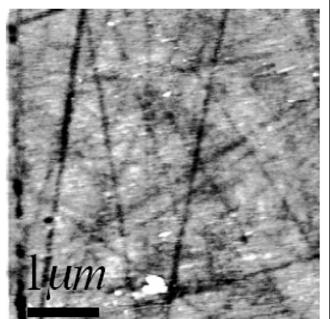
10 AFM: C-face MEG C-face, HV (~10-5 Torr) RF induction furnace ~1450 C, 7 min. See M. Ruan W26.011


.")


11 Graphene Growth Gambaz et al, Carbon 46, 841 (2008). Furnace Growth C-face ~ 0.2nm ~ 0.02nm 9 x 9 m Exfoliaded 400 x 400nm At least one sheet continuously covers the entire surface
12 Important notes on furnace grown epitaxial graphene. 1. The GIT furnace grown graphene crystals are exceptionally well-formed compared to UHV grown material with is of poor quality 2. At least the top layer is continuous over the entire surface making MEG graphene crystals by far the largest quasi 2D crystals known. 3. The number of layers varies (at most) by about 1 layer in well-made samples. 4. The interface layer is n doped and probably more disordered than the other layers.

13 20 layers 2D width: 22 cm -1 No D band 2D-Peak cm -1 Lorentzian fit 23 cm -1 Raman Spectroscopy G-Peak cm -1 A. C. Ferrari et.al. PRL 97, (2006)
14 Stacking Si face: Bernal (AB) C-face Rotational stacking (Multilayered epitaxial graphene)
")

15 Graphene/SiC Commensurability (LEED) SiC bulk Graphene Diffuse Graphene ring SiC bulk (6 3 x 6 3) SiC R30º Si-Face UHV grown 69.1eV C-Face furnace grown 72.2eV Graphene Surface X-ray Diffraction R-2.204º R2.204º R30º
 30 0 (aligned with SiC) 2.2 30 27.8 27.")

16 Graphene/Graphene Commensurability (aligned with SiC) 30 0 (aligned with SiC) º = graphene-graphene commensurate cell 2.2º = graphene-sic commensurate cell 8.9Å Si-face Graphite (AB stacked) C-face (rotated phases)
 G R46.")


17 STM evidence for rotated phases ( 13 x 13) G R46.1º 8.9 Å 5 Å Sample bias: -800 mv Tunneling current: 100 pa 2 sheets with a relative rotation of J. Hass, et al. Phys. Rev. Lett (2008)
R30 100 80 (2 21 2 21)R10.")
 26")
18 Substrate induced rotations SiC Å X 160Å data ( )R ( )R10.9 ( )R (relative to SiC) (relative to SiC)

19 20nmX20nm Miller et al Science, In print 3.8nmX3.8nm 47nmX47nm
20 Rotational Domain Boundaries Atomically flat and continuous across boundary 400 nm 50 pm Joseph A. Stroscio


21 Rotational Domain Boundaries 20 nm 8 nm Joseph A. Stroscio joseph.stroscio@nist.gov


22 Rotational domains (LEEM) 10 m 72.2eV Ellipsometery thickness map: 10±1 layer E.Conrad, M.Sprinkle
23 The Dirac cone


24 Graphene band structure Dirac Point H = v F ˆ p ˆ = ( ˆ x, ˆ y, ˆ x = 0 1 ; 1 0 y = 0 i ; i 0 z = z ) Velocity is constant E =±v F p Neutrino-like dispersion
 n=1 n=2 n=3 n= Graphene on Si-face: gap is observed; Gap closes as")
25 Substrate-induced band gap in Si-face EG Zhou, Gweon, Fedorov, First, de Heer, Lee, Guinea,. Castro Neto, Lanzara Nature Materials 6, (2007) n=1 n=2 n=3 n= Graphene on Si-face: gap is observed; Gap closes as the number of layers increases.


26 Rotations preserve sublattice symmetry Isolated graphene sheet Graphite bilayer R30/R2 fault pair


 Each")

27 T=6K; near K-point ARPES: MEG (C-face) E D - E F ~ 20 mev ± 10meV n~ 10 9 /cm 2 (essentially undoped) Each rotated sheet displays linear dispersion!

 0.99 F (ave.) = 0.87 ±.")
 = 0.86 10 6 m/s -0.16-0.")
28 Layer Interactions (MEG) ~40meV?? F These two sheets are ~3-4Å apart v (right) 0.99 F (ave.) = 0.87 ± m/s v (left) = 0.81 ±.02 F (graphite) = m/s k(a -1 )


29 Spectro-microscopy of single and multi-layer graphene supported by a weakly interacting substrate Knox, Wang, Morgante, Cvetko, Locatelli, Onur Mentes, Angel Ni, Philip Kim, Osgood ARPES of exfoliated graphene: does it have a Dirac point?
")
30 Scanning tunneling spectroscopy of Landau levels Observing the Quantization of Zero Mass Carriers in (Multilayer Epitaxial ) Graphene Science In Press D.L. Miller, K. D. Kubista, G. M. Rutter, M.Ruan, Walt A. de Heer, P. N. First, J. A. Stroscio (NIST, GIT)
31 Previous STS Measurements on Graphite Surfaces Complex spectra Mixture of peaks of linear and nonlinear in B T. Matsui et al. PRL (2005) G. Li and E. Andrei Nature Phys. (2007) Courtesy Joe Stroscio

 2 n=0, 1.")

32 Landau Levels in Graphene Density of states vs E, B Magnetic Field B=8T E = n eh% c n B ± n 2 sgn( ) 2 n=0, 1... Graphene heb E ( 1/2) n = n+ n 0 * m Standard 2DEG Energy (mev) Courtesy P.N.FIrst
33 STS Multilayer Epitaxial Graphene: Landau Levels
34 E n E 0 (mev) LL 0 shift c* = 1.13 x 10⁶ m/s
35 Landau Level Fit T=4K Simple sum of Voigt functions (Gaussian, Lorentzian convolution) Gaussian: 2.8 mev (instrument function + thermal broadening; fixed) LL 0 Lorentzian: 1.5 mev (0.4 ps lifetime: lower limit to momentum relaxation time)
 Density of states vs E, B Magnetic Field Energy (mev) Courtesy P.N.")
36 Tunneling Magnetoconductance Oscillations (~SdH oscillations, but not restricted to E F ) Density of states vs E, B Magnetic Field Energy (mev) Courtesy P.N.FIrst

37 Tunneling Magnetoconductance Oscillations Analogous to SdH oscillations


38 E vs B Fit with v= 1.07*10^6,
39 Landau Index n Fan Plots n B -1 (T -1 ) E = n eh% c n B ± 2 sgn( ) 2 n=0, 1... LL index vs 1/B for different energies
40 Dispersion E(k) c* = (1.070 ± 0.007) x 10 6 Slight asymmetry 2 E = sgn( n) 2 eh c% n B n=0, ± 1... = c% n h k


41 ARPES: C-face MEG vf = 0.87 ± m/s ED - EF ~ 20 ± 10 mev

42 Landau level spectroscopy
43 Courtesy C. Faugeras

44
45 Bands in a magnetic field : Landau level Energy quantization 2 r c n F r c =p/eb F =2 /k F B Normal electrons: quadratic E(k) B B Dirac particles: linear E(k) Energy Energy 3 n E F Magnetic field E n = (n ) heb m * Magnetic field E n =± 2ehc 2 Bn

46 Landau Spectra of C-face Graphene (B) line Transition energy (mev) E F E n =± 2ehc 2 Bn Transmission layers 9-10 layers 50 layers B=1.5T 1.4T 1.5T 1.5T 0.8 HOPG ~ μm B(T 1/2 ) Wavenumber (cm) -1 M. Potemski, G.Martinez, CNRS-LCMI


47 IR cyclotron resonance spectroscopy E F PRL accepted >250,000

48 IR cyclotron resonance spectroscopy LL s visible at RT below 1T.
49 MEG Landau Levels Temperature Independent LL s. Temperature Independent widths Boltzmann population of levels Weak Electron-Phonon Coupling: >250,000 at RT
50 Transport

51 Epitaxial Graphene on 4H-SiC SiC C-Face termination SiC C-face Multilayer Epitaxial Graphene (MEG) ML Si-face Ultrathin Graphite 1-5 ML Si-Face termination n~10 9 /cm 2 Graphene layers Uncharged MEG n~10 12 /cm 2 SiC E Charged interface graphene layer C-face
52 Magneto-transport of 1-2 graphene layers on Si-face Hall bar 400X800 m Si-face, UHV grown, =1000 Rxx ( /sq) 0.3-4K Rxy ( ) Landau index (n) Landau plot n s = cm -2 (same as from xy ) 1/B n (T -1 ) Berry s phase= Rxy ( ) n=3 xy =1.8k Berger et al. J. Chem. Phys. 2004
= 2neBv 2 0 ) Confinement: E n (W)=n v 0 /W Confined Landau levels: E n (B,W) [E n (W) 4")
53 T=4,6, 9, 15, 35 and 58 K; -9 T B 9 T. C-face Hall bar 1 mx200 nm *=27000cm 2 /Vs. Landau levels: E n (B)= 2neBv 2 0 ) Confinement: E n (W)=n v 0 /W Confined Landau levels: E n (B,W) [E n (W) 4 +E n (B) 4 ] 1/4 Berry s phase=
54 Magnetotransport: graphene like; Berry s phase = (No QHE) Hall bar C-face R ( ) R xx ( /sq) 1 m x 6.5 m R= 502 /sq = cm 2 /Vs Landau level index 1/B (T -1 ) R/R=4% Field (T) 100 mk Shubnikov de Haas oscillations Landau level index 1/B (T -1 ) Solid State Com. 2007,Grenoble/GIT collaboration
55 Weak anti-localization (WAL) 4.2 K WAL Theory WL 4.2 K C-face Hall bar
 μ 9000 cm 2 /Vs n s =1.")
56 Magnetotransport of ~1 graphene sheet on C-face Cross etched in a flat terrace xy 2.5 m (k ) μ 9000 cm 2 /Vs n s = cm -2 xx xx (k ) Field(T)
. Resistance is at its theoretical minumum (no boundary scattering!) Oscillations periodic in the magnetic field are seen.")
57 Anomalous Conductance Transition A reversible, reproducible, drop in the conductivity is observed at 200K. The resistance is at its theoretical minimum. Transport is phase coherent over the entire structure (0.5X5 μm). Resistance is at its theoretical minumum (no boundary scattering!) Oscillations periodic in the magnetic field are seen Temperature (K) Could this be the Hoffstadter butterfly? (Moire with a 20 nm lattice constant)
58 Devices
 5 0 xy (Hall)(k ) 1.")
59 The Dirac point E F E D xx (Resistance)(k ) K -5 Tesla Negative Hall (holes) Dirac point Positive Hall (electrons) 5 0 xy (Hall)(k ) 1.5 mx12 m Top gated Hall bar, Si face G D S G V g (V) -5
 10 0 0.6 0.5 0.4 0.3 0.2 1.5x12.")

60 Top and side gated FETs Si-face Top gate g1 Top gated FET g2 Resistance (k /sq) x12.5 m C-face Top gate 3.5x12.5 m s Side gated FET g1 g3 d C-face Side gate d x1 m Gate Voltage (V) The first epitaxial graphene transistors S g2


61 Production process SiC blank Hydrogen etch Device Integration Pattern

62 Final Device Geometry SiC Pt Source Al gate (next level) L=10um W=5um Gr Al SiC Pt Drain Al HfO 2 SiC Graphene Device description and cross section Nominal device Graphene/SiC active layer (C-side), L = 10um, W = 5 um, ridge parallel, 50nm HfO 2 dielectric, Al gate Microscope image shown before gate lift-off J. Kedzierski, P. L. Hsu, P. Hea ley, P. W. Wyatt, C. L. Keast, M. Sprinkle, C. Berger, W. A. de Heer, Epitaxial graphene transistors on SIC substrates,ieee T Electron Dev 55, 2078 (2008).
63 Set of Identical Devices (Si-face) d (1/Ohms) 1.4m 1.2m 1.0m GraphC W2 Si T HfO2 = 40nm W=5μm, L=10μm Minimum conductivity 130uS to 250uS Field Effect Mobility values cm 2 /Vs I on /I off ~ V g (V) Drain current vs. gate voltage at V d = 0.5V J. Kedzierski, P. L. Hsu, P. Hea ley, P. W. Wyatt, C. L. Keast, M. Sprinkle, C. Berger, W. A. de Heer, Epitaxial graphene transistors on SIC substrates,ieee T Electron Dev 55, 2078 (2008).


64 Lithography 98 ribbons per 3.5 x 4.5 mm chip Hall bars and 2-point devices
Tutorial T5 Will Carbon Replace Silicon? The future of graphitic electronics.
 Tutorial T5 Will Carbon Replace Silicon? The future of graphitic electronics. 1:30-2:20 Jim Meindl Nanoelectronics in Retrospect and Prospect 2:20-3:10 Millie Dresselhaus From Graphene to Graphite to Nanotubes
Exceptional ballistic transport in epigraphene. Walt de Heer Georgia Institute of Technology
 Exceptional ballistic transport in epigraphene Walt de Heer Georgia Institute of Technology Program Objective First formulated in 2001 and patented in 2003, our objective is to develop nanoelectronics
Magnetotransport in high mobility epitaxial graphene
 Early View publication on www.interscience.wiley.com (issue and page numbers not yet assigned; citable using Digital Object Identifier DOI) Original phys. stat. sol. (a), 1 5 (2007) / DOI 10.1002/pssa.200675352
Graphite, graphene and relativistic electrons
 Graphite, graphene and relativistic electrons Introduction Physics of E. graphene Y. Andrei Experiments Rutgers University Transport electric field effect Quantum Hall Effect chiral fermions STM Dirac
Optimizing Graphene Morphology on SiC(0001)
") Optimizing Graphene Morphology on SiC(0001) James B. Hannon Rudolf M. Tromp Graphene sheets Graphene sheets can be formed into 0D,1D, 2D, and 3D structures Chemically inert Intrinsically high carrier mobility
Optimizing Graphene Morphology on SiC(0001) James B. Hannon Rudolf M. Tromp Graphene sheets Graphene sheets can be formed into 0D,1D, 2D, and 3D structures Chemically inert Intrinsically high carrier mobility
Graphene FETs EE439 FINAL PROJECT. Yiwen Meng Su Ai
 Graphene FETs EE439 FINAL PROJECT Yiwen Meng Su Ai Introduction What is Graphene? An atomic-scale honeycomb lattice made of carbon atoms Before 2004, Hypothetical Carbon Structure Until 2004, physicists
Magneto-spectroscopy of multilayer epitaxial graphene, of graphite and of graphene
 Magneto-spectroscopy of multilayer epitaxial graphene, of graphite and of graphene Marek Potemski Grenoble High Magnetic Field Laboratory, Centre National de la Recherche Scientifique Grenoble, France
Wide-gap Semiconducting Graphene from Nitrogen-seeded SiC
 Wide-gap Semiconducting Graphene from Nitrogen-seeded SiC F. Wang, 1 G. Liu, 2 S. Rothwell, 3 M. Nevius, 1 A. Tejeda, 4, 5 A. Taleb-Ibrahimi, 6 L.C. Feldman, 2 P.I. Cohen, 3 and E.H. Conrad 1 1 School
SiC Graphene Suitable For Quantum Hall Resistance Metrology.
 SiC Graphene Suitable For Quantum Hall Resistance Metrology. Samuel Lara-Avila 1, Alexei Kalaboukhov 1, Sara Paolillo, Mikael Syväjärvi 3, Rositza Yakimova 3, Vladimir Fal'ko 4, Alexander Tzalenchuk 5,
Graphene. Tianyu Ye November 30th, 2011
 Graphene Tianyu Ye November 30th, 2011 Outline What is graphene? How to make graphene? (Exfoliation, Epitaxial, CVD) Is it graphene? (Identification methods) Transport properties; Other properties; Applications;
Magneto-plasmonic effects in epitaxial graphene
 Magneto-plasmonic effects in epitaxial graphene Alexey Kuzmenko University of Geneva Graphene Nanophotonics Benasque, 4 March 13 Collaborators I. Crassee, N. Ubrig, I. Nedoliuk, J. Levallois, D. van der
Graphene and Quantum Hall (2+1)D Physics
D Physics") The 4 th QMMRC-IPCMS Winter School 8 Feb 2011, ECC, Seoul, Korea Outline 2 Graphene and Quantum Hall (2+1)D Physics Lecture 1. Electronic structures of graphene and bilayer graphene Lecture 2. Electrons
The 4 th QMMRC-IPCMS Winter School 8 Feb 2011, ECC, Seoul, Korea Outline 2 Graphene and Quantum Hall (2+1)D Physics Lecture 1. Electronic structures of graphene and bilayer graphene Lecture 2. Electrons
A BIT OF MATERIALS SCIENCE THEN PHYSICS
 GRAPHENE AND OTHER D ATOMIC CRYSTALS Andre Geim with many thanks to K. Novoselov, S. Morozov, D. Jiang, F. Schedin, I. Grigorieva, J. Meyer, M. Katsnelson A BIT OF MATERIALS SCIENCE THEN PHYSICS CARBON
Dirac fermions in Graphite:
 Igor Lukyanchuk Amiens University, France, Yakov Kopelevich University of Campinas, Brazil Dirac fermions in Graphite: I. Lukyanchuk, Y. Kopelevich et al. - Phys. Rev. Lett. 93, 166402 (2004) - Phys. Rev.
Reduction of Fermi velocity in folded graphene observed by resonance Raman spectroscopy
 Reduction of Fermi velocity in folded graphene observed by resonance Raman spectroscopy Zhenhua Ni, Yingying Wang, Ting Yu, Yumeng You, and Zexiang Shen* Division of Physics and Applied Physics, School
Supplementary Figure 1 Magneto-transmission spectra of graphene/h-bn sample 2 and Landau level transition energies of three other samples.
 Supplementary Figure 1 Magneto-transmission spectra of graphene/h-bn sample 2 and Landau level transition energies of three other samples. (a,b) Magneto-transmission ratio spectra T(B)/T(B 0 ) of graphene/h-bn
Supplementary Figure S1. AFM images of GraNRs grown with standard growth process. Each of these pictures show GraNRs prepared independently,
 Supplementary Figure S1. AFM images of GraNRs grown with standard growth process. Each of these pictures show GraNRs prepared independently, suggesting that the results is reproducible. Supplementary Figure
Self-Doping Effects in Epitaxially-Grown Graphene. Abstract
 Self-Doping Effects in Epitaxially-Grown Graphene D.A.Siegel, 1,2 S.Y.Zhou, 1,2 F.ElGabaly, 3 A.V.Fedorov, 4 A.K.Schmid, 3 anda.lanzara 1,2 1 Department of Physics, University of California, Berkeley,
arxiv: v1 [cond-mat.mtrl-sci] 3 May 2015
![arxiv: v1 [cond-mat.mtrl-sci] 3 May 2015](/thumbs/94/118238290.jpg "arxiv: v1 [cond-mat.mtrl-sci] 3 May 2015") Semiconducting graphene from highly ordered substrate interactions M.S. Nevius,1 M. Conrad,1 F. Wang,1 A. Celis,2, 3 M.N. Nair,4 A. Taleb-Ibrahimi,4 A. Tejeda,2, 3 and E.H. Conrad1, 1 arxiv:1505.00435v1
Semiconducting graphene from highly ordered substrate interactions M.S. Nevius,1 M. Conrad,1 F. Wang,1 A. Celis,2, 3 M.N. Nair,4 A. Taleb-Ibrahimi,4 A. Tejeda,2, 3 and E.H. Conrad1, 1 arxiv:1505.00435v1
Supplementary Information
 Supplementary Information Supplementary Figure 1 AFM and Raman characterization of WS 2 crystals. (a) Optical and AFM images of a representative WS 2 flake. Color scale of the AFM image represents 0-20
Bloch, Landau, and Dirac: Hofstadter s Butterfly in Graphene. Philip Kim. Physics Department, Columbia University
 Bloch, Landau, and Dirac: Hofstadter s Butterfly in Graphene Philip Kim Physics Department, Columbia University Acknowledgment Prof. Cory Dean (now at CUNY) Lei Wang Patrick Maher Fereshte Ghahari Carlos
Carbon based Nanoscale Electronics
 Carbon based Nanoscale Electronics 09 02 200802 2008 ME class Outline driving force for the carbon nanomaterial electronic properties of fullerene exploration of electronic carbon nanotube gold rush of
GRAPHENE ON THE Si-FACE OF SILICON CARBIDE USER MANUAL
 GRAPHENE ON THE Si-FACE OF SILICON CARBIDE USER MANUAL 1. INTRODUCTION Silicon Carbide (SiC) is a wide band gap semiconductor that exists in different polytypes. The substrate used for the fabrication
Ferromagnetism and Anomalous Hall Effect in Graphene
 Ferromagnetism and Anomalous Hall Effect in Graphene Jing Shi Department of Physics & Astronomy, University of California, Riverside Graphene/YIG Introduction Outline Proximity induced ferromagnetism Quantized
arxiv: v1 [cond-mat.mes-hall] 22 Dec 2011
![arxiv: v1 [cond-mat.mes-hall] 22 Dec 2011](/thumbs/76/73542175.jpg "arxiv: v1 [cond-mat.mes-hall] 22 Dec 2011") Direct Measurement of the Fermi Energy in Graphene Using a Double Layer Structure Seyoung Kim, 1 Insun Jo, 2 D. C. Dillen, 1 D. A. Ferrer, 1 B. Fallahazad, 1 Z. Yao, 2 S. K. Banerjee, 1 and E. Tutuc 1
Direct Measurement of the Fermi Energy in Graphene Using a Double Layer Structure Seyoung Kim, 1 Insun Jo, 2 D. C. Dillen, 1 D. A. Ferrer, 1 B. Fallahazad, 1 Z. Yao, 2 S. K. Banerjee, 1 and E. Tutuc 1
Epitaxial graphene on SiC(0001): More than just honeycombs. Y. Qi, S. H. Rhim, G. F. Sun, M. Weinert, and L. Li*
: More than just honeycombs. Y. Qi, S. H. Rhim, G. F. Sun, M. Weinert, and L. Li*") Epitaxial graphene on SiC(0001): More than just honeycombs Y. Qi, S. H. Rhim, G. F. Sun, M. Weinert, and L. Li* Department of Physics and Laboratory for Surface Studies University of Wisconsin, Milwaukee,
Epitaxial graphene on SiC(0001): More than just honeycombs Y. Qi, S. H. Rhim, G. F. Sun, M. Weinert, and L. Li* Department of Physics and Laboratory for Surface Studies University of Wisconsin, Milwaukee,
Electronic states on the surface of graphite
 Electronic states on the surface of graphite Guohong Li, Adina Luican, Eva Y. Andrei * Department of Physics and Astronomy, Rutgers Univsersity, Piscataway, NJ 08854, USA Elsevier use only: Received date
Large area and structured epitaxial graphene produced by confinement controlled sublimation of silicon carbide
 Large area and structured epitaxial graphene produced by confinement controlled sublimation of silicon carbide Walt. A. de Heer 1, Claire Berger 1, 2, Ming Ruan 1, Mike Sprinkle 1, Xuebin Li 1, Yike Hu
Surface Science 604 (2010) Contents lists available at ScienceDirect. Surface Science. journal homepage:
 Contents lists available at ScienceDirect. Surface Science. journal homepage:") Surface Science 604 (2010) 84 88 Contents lists available at ScienceDirect Surface Science journal homepage: www.elsevier.com/locate/susc Signatures of epitaxial graphene grown on Si-terminated 6H-SiC
Surface Science 604 (2010) 84 88 Contents lists available at ScienceDirect Surface Science journal homepage: www.elsevier.com/locate/susc Signatures of epitaxial graphene grown on Si-terminated 6H-SiC
NiCl2 Solution concentration. Etching Duration. Aspect ratio. Experiment Atmosphere Temperature. Length(µm) Width (nm) Ar:H2=9:1, 150Pa
 Width (nm) Ar:H2=9:1, 150Pa") Experiment Atmosphere Temperature #1 # 2 # 3 # 4 # 5 # 6 # 7 # 8 # 9 # 10 Ar:H2=9:1, 150Pa Ar:H2=9:1, 150Pa Ar:H2=9:1, 150Pa Ar:H2=9:1, 150Pa Ar:H2=9:1, 150Pa Ar:H2=9:1, 150Pa Ar:H2=9:1, 150Pa Ar:H2=9:1,
Experiment Atmosphere Temperature #1 # 2 # 3 # 4 # 5 # 6 # 7 # 8 # 9 # 10 Ar:H2=9:1, 150Pa Ar:H2=9:1, 150Pa Ar:H2=9:1, 150Pa Ar:H2=9:1, 150Pa Ar:H2=9:1, 150Pa Ar:H2=9:1, 150Pa Ar:H2=9:1, 150Pa Ar:H2=9:1,
Spectro-microscopy of single and multi-layer graphene supported by a weakly. interacting substrate
 Spectro-microscopy of single and multi-layer graphene supported by a weakly interacting substrate Kevin R. Knox 1,2, Shancai Wang 2, Alberto Morgante 3,4 Dean Cvetko 3,5, Andrea Locatelli 6, Tevfik Onur
Hydrogenated Graphene
 Hydrogenated Graphene Stefan Heun NEST, Istituto Nanoscienze-CNR and Scuola Normale Superiore Pisa, Italy Outline Epitaxial Graphene Hydrogen Chemisorbed on Graphene Hydrogen-Intercalated Graphene Outline
A. Optimizing the growth conditions of large-scale graphene films
 1 A. Optimizing the growth conditions of large-scale graphene films Figure S1. Optical microscope images of graphene films transferred on 300 nm SiO 2 /Si substrates. a, Images of the graphene films grown
SUPPLEMENTARY INFORMATION
 DOI: 1.138/NMAT3449 Topological crystalline insulator states in Pb 1 x Sn x Se Content S1 Crystal growth, structural and chemical characterization. S2 Angle-resolved photoemission measurements at various
Infrared magneto-spectroscopy of graphene-based systems
 Infrared magneto-spectroscopy of graphene-based systems M. Orlita, C. Faugeras, G. Martinez P. Neugebauer, M. Potemski Laboratoire National des Champs Magnétiques Intenses CNRS, Grenoble, France Collaborators:
XPS Depth Profiling of Epitaxial Graphene Intercalated with FeCl 3
 XPS Depth Profiling of Epitaxial Graphene Intercalated with FeCl 3 Mahdi Ibrahim Maynard H. Jackson High School Atlanta, GA. Faculty Advisor: Dr. Kristin Shepperd Research Group: Prof. Edward Conrad School
GRAPHENE the first 2D crystal lattice
 GRAPHENE the first 2D crystal lattice dimensionality of carbon diamond, graphite GRAPHENE realized in 2004 (Novoselov, Science 306, 2004) carbon nanotubes fullerenes, buckyballs what s so special about
(Suppression of) Dephasing in a Field-Effect Black Phosphorus Transistor. Guillaume Gervais (Physics) and Thomas Szkopek (Electrical Eng.
 Dephasing in a Field-Effect Black Phosphorus Transistor. Guillaume Gervais (Physics) and Thomas Szkopek (Electrical Eng.") (Suppression of) Dephasing in a Field-Effect Black Phosphorus Transistor Guillaume Gervais (Physics) and Thomas Szkopek (Electrical Eng.) July 28, 2016 This talk contains no quantum Hall effect at all
(Suppression of) Dephasing in a Field-Effect Black Phosphorus Transistor Guillaume Gervais (Physics) and Thomas Szkopek (Electrical Eng.) July 28, 2016 This talk contains no quantum Hall effect at all
Graphene films on silicon carbide (SiC) wafers supplied by Nitride Crystals, Inc.
 wafers supplied by Nitride Crystals, Inc.") 9702 Gayton Road, Suite 320, Richmond, VA 23238, USA Phone: +1 (804) 709-6696 info@nitride-crystals.com www.nitride-crystals.com Graphene films on silicon carbide (SiC) wafers supplied by Nitride Crystals,
9702 Gayton Road, Suite 320, Richmond, VA 23238, USA Phone: +1 (804) 709-6696 info@nitride-crystals.com www.nitride-crystals.com Graphene films on silicon carbide (SiC) wafers supplied by Nitride Crystals,
Landau Quantization in Graphene Monolayer, Bernal Bilayer, and Bernal
 Landau Quantization in Graphene Monolayer, Bernal Bilayer, and Bernal Trilayer on Graphite Surface Long-Jing Yin, Si-Yu Li, Jia-Bin Qiao, Jia-Cai Nie, Lin He * Electronic properties of surface areas decoupled
Large area and structured epitaxial graphene produced by confinement controlled sublimation of silicon carbide
 Large area and structured epitaxial graphene produced by confinement controlled sublimation of silicon carbide Walt A. de Heer a,1, Claire Berger a,b, Ming Ruan a, Mike Sprinkle a, Xuebin Li a, Yike Hu
Supplementary Figures
 Supplementary Figures 1500 Heating Annealing Growing Cooling 20 Temperature ( o C) 1000 500 Ar:H 2 = 5:1 Ar:H 2 = 5:1 15 10 5 Pressure(Pa) 0 Ar(SiH 4 (5%)):C 2 H 2 = 1:2 120 mins 5 mins 5 40 mins ~120
Scanning tunneling microscopy and spectroscopy of graphene layers on graphite
 Scanning tunneling microscopy and spectroscopy of graphene layers on graphite Adina Luican, Guohong Li and Eva Y. Andrei Department of Physics and Astronomy, Rutgers University, Piscataway, New Jersey
New Quantum Transport Results in Type-II InAs/GaSb Quantum Wells
 New Quantum Transport Results in Type-II InAs/GaSb Quantum Wells Wei Pan Sandia National Laboratories Sandia National Laboratories is a multi-program laboratory managed and operated by Sandia Corporation,
SUPPLEMENTARY INFORMATION
 SUPPLEMENTARY INFORMATION Towards wafer-size graphene layers by atmospheric pressure graphitization of silicon carbide Supporting online material Konstantin V. Emtsev 1, Aaron Bostwick 2, Karsten Horn
Graphene: Plane and Simple Electrical Metrology?
 Graphene: Plane and Simple Electrical Metrology? R. E. Elmquist, F. L. Hernandez-Marquez, M. Real, T. Shen, D. B. Newell, C. J. Jacob, and G. R. Jones, Jr. National Institute of Standards and Technology,
Probing Dirac Fermions in Graphene by Scanning Tunneling Probes
 Probing Dirac Fermions in Graphene by Scanning Tunneling Probes Adina Luican-Mayer and Eva Y. Andrei Department of Physics and Astronomy, Rutgers University, Piscataway, NJ 08854, USA Abstract Graphene
Supporting Information. by Hexagonal Boron Nitride
 Supporting Information High Velocity Saturation in Graphene Encapsulated by Hexagonal Boron Nitride Megan A. Yamoah 1,2,, Wenmin Yang 1,3, Eric Pop 4,5,6, David Goldhaber-Gordon 1 * 1 Department of Physics,
Supplementary Materials for
 advances.sciencemag.org/cgi/content/full/3/10/e1701661/dc1 Supplementary Materials for Defect passivation of transition metal dichalcogenides via a charge transfer van der Waals interface Jun Hong Park,
1. Nanotechnology & nanomaterials -- Functional nanomaterials enabled by nanotechnologies.
 Novel Nano-Engineered Semiconductors for Possible Photon Sources and Detectors NAI-CHANG YEH Department of Physics, California Institute of Technology 1. Nanotechnology & nanomaterials -- Functional nanomaterials
Supplementary Figure 1 Experimental setup for crystal growth. Schematic drawing of the experimental setup for C 8 -BTBT crystal growth.
 Supplementary Figure 1 Experimental setup for crystal growth. Schematic drawing of the experimental setup for C 8 -BTBT crystal growth. Supplementary Figure 2 AFM study of the C 8 -BTBT crystal growth
Energy Spectroscopy. Ex.: Fe/MgO
 Energy Spectroscopy Spectroscopy gives access to the electronic properties (and thus chemistry, magnetism,..) of the investigated system with thickness dependence Ex.: Fe/MgO Fe O Mg Control of the oxidation
.Fritjaf Capra, The Tao of Physics
 Probing inside the atom and investigating its structure, science transcended the limits of our sensory imagination. From this point on, it could no longer rely with absolute certainty on logic and common
Anisotropic spin splitting in InGaAs wire structures
 Available online at www.sciencedirect.com Physics Physics Procedia Procedia 3 (010) 00 (009) 155 159 000 000 14 th International Conference on Narrow Gap Semiconductors and Systems Anisotropic spin splitting
Scanning Tunneling Microscopy & Spectroscopy: A tool for probing electronic inhomogeneities in correlated systems
 Scanning Tunneling Microscopy & Spectroscopy: A tool for probing electronic inhomogeneities in correlated systems Anjan K. Gupta Physics Department, I. I. T Kanpur ICTS-GJ, IITK, Feb 2010 Acknowledgements
Supplementary Figure 1: MoS2 crystals on WSe2-EG and EG and WSe2 crystals on MoSe2-EG and EG.
 Supplementary Figure 1: MoS2 crystals on WSe2-EG and EG and WSe2 crystals on MoSe2-EG and EG. (a) The MoS2 crystals cover both of EG and WSe2/EG after the CVD growth (Scar bar: 400 nm) (b) shows TEM profiles
Observation of topological surface state quantum Hall effect in an intrinsic three-dimensional topological insulator
 Observation of topological surface state quantum Hall effect in an intrinsic three-dimensional topological insulator Authors: Yang Xu 1,2, Ireneusz Miotkowski 1, Chang Liu 3,4, Jifa Tian 1,2, Hyoungdo
STM and graphene. W. W. Larry Pai ( 白偉武 ) Center for condensed matter sciences, National Taiwan University NTHU, 2013/05/23
 Center for condensed matter sciences, National Taiwan University NTHU, 2013/05/23") STM and graphene W. W. Larry Pai ( 白偉武 ) Center for condensed matter sciences, National Taiwan University NTHU, 2013/05/23 Why graphene is important: It is a new form of material (two dimensional, single
STM and graphene W. W. Larry Pai ( 白偉武 ) Center for condensed matter sciences, National Taiwan University NTHU, 2013/05/23 Why graphene is important: It is a new form of material (two dimensional, single
Epitaxial graphene. Abstract
 Epitaxial graphene Walt A. de Heer a, Claire Berger a,b Xiaosong Wu a Phillip N. First a Edward H. Conrad a Xuebin Li a Tianbo Li a Michael Sprinkle a Joanna Hass a Marcin L. Sadowski b Marek Potemski
Spin-orbit Effects in Semiconductor Spintronics. Laurens Molenkamp Physikalisches Institut (EP3) University of Würzburg
 University of Würzburg") Spin-orbit Effects in Semiconductor Spintronics Laurens Molenkamp Physikalisches Institut (EP3) University of Würzburg Collaborators Hartmut Buhmann, Charlie Becker, Volker Daumer, Yongshen Gui Matthias
Spin-orbit Effects in Semiconductor Spintronics Laurens Molenkamp Physikalisches Institut (EP3) University of Würzburg Collaborators Hartmut Buhmann, Charlie Becker, Volker Daumer, Yongshen Gui Matthias
Electronic Properties of Hydrogenated Quasi-Free-Standing Graphene
 GCOE Symposium Tohoku University 2011 Electronic Properties of Hydrogenated Quasi-Free-Standing Graphene Danny Haberer Leibniz Institute for Solid State and Materials Research Dresden Co-workers Supervising
Graphene Novel Material for Nanoelectronics
 Graphene Novel Material for Nanoelectronics Shintaro Sato Naoki Harada Daiyu Kondo Mari Ohfuchi (Manuscript received May 12, 2009) Graphene is a flat monolayer of carbon atoms with a two-dimensional honeycomb
Quantum Hall Effect in Graphene p-n Junctions
 Quantum Hall Effect in Graphene p-n Junctions Dima Abanin (MIT) Collaboration: Leonid Levitov, Patrick Lee, Harvard and Columbia groups UIUC January 14, 2008 Electron transport in graphene monolayer New
Surface atoms/molecules of a material act as an interface to its surrounding environment;
 1 Chapter 1 Thesis Overview Surface atoms/molecules of a material act as an interface to its surrounding environment; their properties are often complicated by external adsorbates/species on the surface
Quantum Condensed Matter Physics Lecture 12
 Quantum Condensed Matter Physics Lecture 12 David Ritchie QCMP Lent/Easter 2016 http://www.sp.phy.cam.ac.uk/drp2/home 12.1 QCMP Course Contents 1. Classical models for electrons in solids 2. Sommerfeld
Scanning Tunneling Microscopy Studies of Topological Insulators Grown by Molecular Beam Epitaxy
 EPJ Web of Conferences 23, 00020 ( 2012) DOI: 10.1051/ epjconf/ 20122300020 C Owned by the authors, published by EDP Sciences, 2012 Scanning Tunneling Microscopy Studies of Topological Insulators Grown
Supplementary Figure 1 Dark-field optical images of as prepared PMMA-assisted transferred CVD graphene films on silicon substrates (a) and the one
 and the one") Supplementary Figure 1 Dark-field optical images of as prepared PMMA-assisted transferred CVD graphene films on silicon substrates (a) and the one after PBASE monolayer growth (b). 1 Supplementary Figure
Supplementary Figure 1 Dark-field optical images of as prepared PMMA-assisted transferred CVD graphene films on silicon substrates (a) and the one after PBASE monolayer growth (b). 1 Supplementary Figure
Supplementary Figure 2 Photoluminescence in 1L- (black line) and 7L-MoS 2 (red line) of the Figure 1B with illuminated wavelength of 543 nm.
 and 7L-MoS 2 (red line) of the Figure 1B with illuminated wavelength of 543 nm.") PL (normalized) Intensity (arb. u.) 1 1 8 7L-MoS 1L-MoS 6 4 37 38 39 4 41 4 Raman shift (cm -1 ) Supplementary Figure 1 Raman spectra of the Figure 1B at the 1L-MoS area (black line) and 7L-MoS area (red
PL (normalized) Intensity (arb. u.) 1 1 8 7L-MoS 1L-MoS 6 4 37 38 39 4 41 4 Raman shift (cm -1 ) Supplementary Figure 1 Raman spectra of the Figure 1B at the 1L-MoS area (black line) and 7L-MoS area (red
SUPPLEMENTARY INFORMATION
 Dirac electron states formed at the heterointerface between a topological insulator and a conventional semiconductor 1. Surface morphology of InP substrate and the device Figure S1(a) shows a 10-μm-square
TOPOLOGICAL BANDS IN GRAPHENE SUPERLATTICES
 TOPOLOGICAL BANDS IN GRAPHENE SUPERLATTICES 1) Berry curvature in superlattice bands 2) Energy scales for Moire superlattices 3) Spin-Hall effect in graphene Leonid Levitov (MIT) @ ISSP U Tokyo MIT Manchester
SUPPLEMENTARY INFORMATION
 SUPPLEMENTARY INFORMATION SUPPLEMENTARY INFORMATION Trilayer graphene is a semimetal with a gate-tuneable band overlap M. F. Craciun, S. Russo, M. Yamamoto, J. B. Oostinga, A. F. Morpurgo and S. Tarucha
SUPPLEMENTARY INFORMATION
 Dirac cones reshaped by interaction effects in suspended graphene D. C. Elias et al #1. Experimental devices Graphene monolayers were obtained by micromechanical cleavage of graphite on top of an oxidized
Physics in two dimensions in the lab
 Physics in two dimensions in the lab Nanodevice Physics Lab David Cobden PAB 308 Collaborators at UW Oscar Vilches (Low Temperature Lab) Xiaodong Xu (Nanoscale Optoelectronics Lab) Jiun Haw Chu (Quantum
Surface Science Reports. The surface science of graphene: Metal interfaces, CVD synthesis, nanoribbons, chemical modifications, and defects
 Surface Science Reports 67 (2012) 83 115 Contents lists available at SciVerse ScienceDirect Surface Science Reports journal homepage: www.elsevier.com/locate/surfrep The surface science of graphene: Metal
Graphene Fundamentals and Emergent Applications
 Graphene Fundamentals and Emergent Applications Jamie H. Warner Department of Materials University of Oxford Oxford, UK Franziska Schaffel Department of Materials University of Oxford Oxford, UK Alicja
Impact of disorder and topology in two dimensional systems at low carrier densities
 Impact of disorder and topology in two dimensional systems at low carrier densities A Thesis Submitted For the Degree of Doctor of Philosophy in the Faculty of Science by Mohammed Ali Aamir Department
Highly Sensitive and Wide-Band Tunable Terahertz Response of Plasma Wave based on Graphene Field Effect Transistors
 Supplementary Information Highly Sensitive and Wide-Band Tunable Terahertz Response of Plasma Wave based on Graphene Field Effect Transistors Lin Wang, Xiaoshuang Chen *, Anqi Yu, Yang Zhang, Jiayi Ding
Yugang Sun Center for Nanoscale Materials, Argonne National Laboratory, Argonne, IL 60439
 Morphology of Graphene on SiC( 000 1 ) Surfaces Luxmi, P. J. Fisher, N. Srivastava, and R. M. Feenstra Dept. Physics, Carnegie Mellon University, Pittsburgh, PA 15213 Yugang Sun Center for Nanoscale Materials,
Quantum Confinement in Graphene
 Quantum Confinement in Graphene from quasi-localization to chaotic billards MMM dominikus kölbl 13.10.08 1 / 27 Outline some facts about graphene quasibound states in graphene numerical calculation of
CHARACTERISTICS OF GRAPHITE FILMS ON SILICON- AND CARBON- TERMINATED FACES OF SILICON CARBIDE
 CHARACTERISTICS OF GRAPHITE FILMS ON SILICON- AND CARBON- TERMINATED FACES OF SILICON CARBIDE A Thesis Presented to The Academic Faculty by Tianbo Li In Partial Fulfillment of the Requirements for the
Initial Stages of Growth of Organic Semiconductors on Graphene
 Initial Stages of Growth of Organic Semiconductors on Graphene Presented by: Manisha Chhikara Supervisor: Prof. Dr. Gvido Bratina University of Nova Gorica Outline Introduction to Graphene Fabrication
Transport through Andreev Bound States in a Superconductor-Quantum Dot-Graphene System
 Transport through Andreev Bound States in a Superconductor-Quantum Dot-Graphene System Nadya Mason Travis Dirk, Yung-Fu Chen, Cesar Chialvo Taylor Hughes, Siddhartha Lal, Bruno Uchoa Paul Goldbart University
SUPPLEMENTARY INFORMATION
 doi:1.138/nature12186 S1. WANNIER DIAGRAM B 1 1 a φ/φ O 1/2 1/3 1/4 1/5 1 E φ/φ O n/n O 1 FIG. S1: Left is a cartoon image of an electron subjected to both a magnetic field, and a square periodic lattice.
High Electron Mobility in Epitaxial Graphene on 4H-SiC(0001) via post-growth annealing under hydrogen
 via post-growth annealing under hydrogen") High Electron Mobility in Epitaxial Graphene on 4H-SiC(0001) via post-growth annealing under hydrogen E. Pallecchi 1, F. Lafont 2, V. Cavaliere 1, F. Schopfer 2, D. Mailly 1, W. Poirier 2 and A. Ouerghi
High Electron Mobility in Epitaxial Graphene on 4H-SiC(0001) via post-growth annealing under hydrogen E. Pallecchi 1, F. Lafont 2, V. Cavaliere 1, F. Schopfer 2, D. Mailly 1, W. Poirier 2 and A. Ouerghi
(a) (b) Supplementary Figure 1. (a) (b) (a) Supplementary Figure 2. (a) (b) (c) (d) (e)
 (b) Supplementary Figure 1. (a) (b) (a) Supplementary Figure 2. (a) (b) (c) (d) (e)") (a) (b) Supplementary Figure 1. (a) An AFM image of the device after the formation of the contact electrodes and the top gate dielectric Al 2 O 3. (b) A line scan performed along the white dashed line
(a) (b) Supplementary Figure 1. (a) An AFM image of the device after the formation of the contact electrodes and the top gate dielectric Al 2 O 3. (b) A line scan performed along the white dashed line
Scalable templated growth of graphene nanoribbons on SiC
 Scalable templated growth of graphene nanoribbons on SiC Mike Sprinkle, Ming Ruan, Yike Hu, John H. Hankinson, Miguel Rubio-Roy, Baiqian Zhang, Xiaosong Wu, Claire Berger, Walt. A. De Heer To cite this
SUPPLEMENTARY INFORMATION
 DOI: 1.138/NNANO.211.214 Control over topological insulator photocurrents with light polarization J.W. McIver*, D. Hsieh*, H. Steinberg, P. Jarillo-Herrero and N. Gedik SI I. Materials and device fabrication
Center for Integrated Nanostructure Physics (CINAP)
") Center for Integrated Nanostructure Physics (CINAP) - Institute for Basic Science (IBS) was launched in 2012 by the Korean government to promote basic science in Korea - Our Center was established in 2012
Center for Integrated Nanostructure Physics (CINAP) - Institute for Basic Science (IBS) was launched in 2012 by the Korean government to promote basic science in Korea - Our Center was established in 2012
Soft Carrier Multiplication by Hot Electrons in Graphene
 Soft Carrier Multiplication by Hot Electrons in Graphene Anuj Girdhar 1,3 and J.P. Leburton 1,2,3 1) Department of Physics 2) Department of Electrical and Computer Engineering, and 3) Beckman Institute
Quantum Hall effect and Landau level crossing of Dirac fermions in trilayer graphene Supplementary Information
 Quantum Hall effect and Landau level crossing of Dirac fermions in trilayer graphene Supplementary Information Thiti Taychatanapat, Kenji Watanabe, Takashi Taniguchi, Pablo Jarillo-Herrero Department of
Broken Symmetry States and Divergent Resistance in Suspended Bilayer Graphene
 Broken Symmetry States and Divergent Resistance in Suspended Bilayer Graphene The Harvard community has made this article openly available. Please share how this access benefits you. Your story matters.
single-layer transition metal dichalcogenides MC2
 single-layer transition metal dichalcogenides MC2 Period 1 1 H 18 He 2 Group 1 2 Li Be Group 13 14 15 16 17 18 B C N O F Ne 3 4 Na K Mg Ca Group 3 4 5 6 7 8 9 10 11 12 Sc Ti V Cr Mn Fe Co Ni Cu Zn Al Ga
The twisted bilayer: an experimental and theoretical review. Graphene, 2009 Benasque. J.M.B. Lopes dos Santos
 Moiré in Graphite and FLG Continuum theory Results Experimental and theoretical conrmation Magnetic Field The twisted bilayer: an experimental and theoretical review J.M.B. Lopes dos Santos CFP e Departamento
Stripes developed at the strong limit of nematicity in FeSe film
 Stripes developed at the strong limit of nematicity in FeSe film Wei Li ( ) Department of Physics, Tsinghua University IASTU Seminar, Sep. 19, 2017 Acknowledgements Tsinghua University Prof. Qi-Kun Xue,
3-month progress Report
 3-month progress Report Graphene Devices and Circuits Supervisor Dr. P.A Childs Table of Content Abstract... 1 1. Introduction... 1 1.1 Graphene gold rush... 1 1.2 Properties of graphene... 3 1.3 Semiconductor
Growing Graphene on Semiconductors
 Growing Graphene on Semiconductors edited by Nunzio Motta Francesca Iacopi Camilla Coletti Growing Graphene on Semiconductors Growing Graphene on Semiconductors edited by Nunzio Motta Francesca Iacopi
Graphene - most two-dimensional system imaginable
 Graphene - most two-dimensional system imaginable A suspended sheet of pure graphene a plane layer of C atoms bonded together in a honeycomb lattice is the most two-dimensional system imaginable. A.J.
SUPPLEMENTARY INFORMATION
 SUPPLEMENTARY INFORMATION doi: 10.1038/nPHYS1463 Observation of Van Hove singularities in twisted graphene layers Guohong Li 1, A. Luican 1, J.M. B. Lopes dos Santos 2, A. H. Castro Neto 3, Alfonso Reina
Epitaxial graphene. 1. Introduction
 Solid State Communications 143 (2007) 92 100 www.elsevier.com/locate/ssc Epitaxial graphene Walt A. de Heer a,, Claire Berger a,b, Xiaosong Wu a, Phillip N. First a, Edward H. Conrad a, Xuebin Li a, Tianbo
Physics of Nanotubes, Graphite and Graphene Mildred Dresselhaus
 Quantum Transport and Dynamics in Nanostructures The 4 th Windsor Summer School on Condensed Matter Theory 6-18 August 2007, Great Park Windsor (UK) Physics of Nanotubes, Graphite and Graphene Mildred