Large area and structured epitaxial graphene produced by confinement controlled sublimation of silicon carbide
|
|
|
- Ferdinand Conley
- 5 years ago
- Views:
Transcription
1 Large area and structured epitaxial graphene produced by confinement controlled sublimation of silicon carbide Walt. A. de Heer 1, Claire Berger 1, 2, Ming Ruan 1, Mike Sprinkle 1, Xuebin Li 1, Yike Hu 1, Baiqian Zhang 1, John Hankinson 1, Edward H. Conrad 1 1 Georgia Institute of Technology, School of Physics, Atlanta, GA , USA 2 CNRS- Institut Néel, Grenoble, France ABSTRACT After the pioneering investigations into graphene-based electronics at Georgia Tech (GT), great strides have been made developing epitaxial graphene on silicon carbide (EG) as a new electronic material. EG has not only demonstrated its potential for large scale applications, it also has become an invaluable material for fundamental twodimensional electron gas physics showing that only EG is on route to define future graphene science. It was long known that graphene mono and multilayers grow on SiC crystals at high temperatures in ultra-high vacuum. At these temperatures, silicon sublimes from the surface and the carbon rich surface layer transforms to graphene. However the quality of the graphene produced in ultrahigh vacuum is poor due to the high sublimation rates at relatively low temperatures. The GT team developed growth methods involving encapsulating the SiC crystals in graphite enclosures, thereby sequestering the evaporated silicon and bringing growth process closer to equilibrium. In this confinement controlled sublimation (CCS) process, very high quality graphene is grown on both polar faces of the SiC crystals. Since 2003, over 50 publications used CCS grown graphene, where it is known as the furnace grown graphene. Graphene multilayers grown on the carbon-terminated face of SiC, using the CCS method, were shown to consist of decoupled high mobility graphene layers. The CCS method is now applied on structured silicon carbide surfaces to produce high mobility nano-patterned graphene structures thereby demonstrating that EG is a viable contender for nextgeneration electronics. Here we present the CCS method and demonstrate several of epitaxial graphene s outstanding properties and applications. Introduction Graphene has been known and studied for decades in many forms, 1, 2, 3 but it was not until 2001 when graphene s potential for electronics was recognized 4, 5. Graphenebased electronics requires a patternable form of graphene with excellent electronic properties. It was clear from the outset 4 that epitaxial graphene on silicon carbide (EG) 2 was the most promising form of graphene for this project. However, EG produced by conventional methods is of poor quality 6. It was clear that much higher quality material would need to be produced for graphene-based electronics to have any chance to be realized. The confinement controlled sublimation (CCS) method that is described here is well on its way to satisfy multiple stringent conditions required for a viable electronic material.
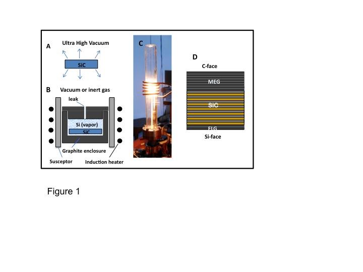
2 Note that the somewhat later parallel development of back-gated exfoliated graphitic flakes deposited on oxidized silicon 7, has little practical impact in the development of graphene electronics. While back-gated graphene flakes are extremely useful for two dimensional electron gas research, randomly deposited graphitic flakes obviously do not constitute an electronic material and back-gating (that switches all devices on the substrate at once) is not useful for electronics. Production of epitaxial graphene Van Bommel first showed in 1975 that a graphene layer grows on hexagonal silicon carbide in ultra high vacuum (UHV) at temperatures above about 800 C. 2 Silicon sublimation from the SiC causes a carbon rich surface that nucleates an epitaxial graphene layer, Fig. 1. The graphene growth rate was found to depend on the specific polar SiC crystal face: graphene forms much slower on the silicon-terminated face (0001) surface (or Si-face) than on the carbon-terminated face (000-1) surface (or C-face). Van Bommel identified monocrystalline graphite monolayer films (i.e. graphene) 2 that were found to be essentially decoupled from the SiC substrate 6 and therefore were electronically equivalent to isolated graphene sheets. 1 Since 1975, these films were referred to as monolayer graphite, or two-dimensional graphite crystals or epitaxial graphene. In fact, electronically decoupled epitaxial graphene had been observed on many surfaces, such as Pt, Ni, Ru, Ir etc 3, but until 2001 the electronic properties and the applications potential of graphene had not been considered. By 2003 the ideas were fully developed and backed with compelling scientific evidence (that was published 5 in 2004). The invention of graphene based electronics was patented in June The first graphene transport measurements were performed on epitaxial graphene films grown by the UHV sublimation method 5, 8. Graphene films produced this way are defective 6 (Fig. 2A) and have low mobilities 5 (!~15 cm 2 V -1 s -1 ). Nonetheless, investigations demonstrated that these epitaxial graphene films could be patterned using standard microelectronics methods and that the films had two-dimensional electron gas properties. By 2003 the UHV sublimation process had been improved to produce monolayer graphene films with mobilities exceeding 10 3 cm 2 V -1 s Magnetotransport measurements of these films showed precursors of the half-integer quantum Hall effect with its characteristic non-trivial Berry s phase 9. While the improvement was significant, these mobilities are still low compared with nanotubes 10 or graphite 11. Defects in UHV sublimed silicon carbide can be traced to the relatively low growth temperatures and the high graphitization rates in the out-of equilibrium UHV sublimation process. While increased growth temperature will anneal vacancies and grain boundaries, the UHV growth method still leads to unacceptable high sublimation rates. There are a number of way to control the rate at which silicon sublimes. For example by supplying silicon in a vapor phase compound (e.g., silane 12 ) or by flowing an inert gas over the hot silicon carbide surface 13.
3 Alternatively, the confinement controlled sublimation method developed at GT relies on confining the silicon carbide in a graphite enclosure (either in vacuum or in an inert gas). This limits the escape of Si and thus maintains a high Si vapor pressure so that graphene growth proceeds close to thermodynamic equilibrium (Fig. 1B). Graphene growth over macroscopic areas can be controlled on both polar faces of SiC to produce either monolayer graphene or multilayer graphene films (Fig. 1E, F). Over 2000 individual CCS epitaxial graphene samples have been made and CCS produced graphene has been characterized in over 50 publications, where it is referred to as furnace grown epitaxial graphene. Particularly relevant examples are the demonstration of infra-red Landau level spectroscopy showing very high moblities 14, quantum Hall effect 15, scanning tunneling Landau level spectroscopy 16, fractional Landau level filling factors 17, and self assembly of graphene ribbons 18 large scale patterning, electronic confinement and coherence 19, electronic structure of decoupled 20, 21 layers in multilayered epitaxial graphene Until now, details of the CCS method have not been published. The principle of CCS can be understood from kinetic gas theory [Fig. 1A, B]. Graphene growth is proportional to the rate of silicon depletion from the SiC surface, since each evaporated silicon atom leaves behind one carbon atom on the surface. In thermodynamic equilibrium the Si evaporation rate, n -, and the Si condensation rate, n + at the SiC are exactly balanced so that graphene does not form. This condition will eventually be established in a hermetically sealed, non-reactive, enclosure at any temperature, after the enclosure surfaces have been passivated. In our design, we use a graphite enclosure and passivation of the enclosure is achieved after several graphene growth cycles. In more detail, assume that a Si atom impinging on the surface condenses with a sticking probability!, ( 0"!"1) then n + =! v ave # eq /4 where v ave ="(8kT/#m) is the average thermal speed of a silicon atom in the vapor, m is its atomic mass and # eq (T) is the vapor density of silicon in equilibrium with silicon carbide at temperature T. Consequently n + $! # eq (2kT/#m) 1/2. The sticking coefficient (but not the vapor density) depends on the local surface structure, and the polar face. For simplicity, in the rest of this discussion we assume!=1, independent of T. However we note that graphene growth rates are greater on the C-face than on the Si face, implying that! is greater on the former than on the latter which is important for certain implementations of the method. Clearly, the silicon must escape through the layers that have already formed, so that the rates depend on the graphene thickness. It appears however, that for thinner layers, silicon manages to readily escape from the silicon carbide surface. If the enclosure is not hermetically sealed, but supplied with a small calibrated leak [Fig. 1B], then n - > n + causing graphene to grow at a rate n gr = n - - n +. Consequently, n gr is controlled by the size of the leak. In general, the rate at which silicon atoms escape is N = C v ave # eq, where C is the effective area of the leak (for a cylindrical hole of diameter D and length L, C=D 3 /3L). Consequently, n gr = N/A where A is the crystal surface area. For example, for a 1 cm 2 crystal in vacuum, with L = 1 cm and D = 0.75 mm the graphene formation rate is reduced by more that a factor of about 1000 compared to the UHV sublimation method (in which n + =0).
4 The actual rates can be estimated from the vapor pressure of P Si (T) of Si over SiC, as has been determined by Lilov 22 : P Si (1500K)= Torr, P Si (2000K)= Torr, P Si (2500K)=1.4 Torr, consequently, P Si and # eq increase by about a factor of 7 per 100K. Assuming the sticking coefficient for the C-face is!=1, and that one carbon atom remains for every evaporated silicon atom, then a graphene monolayer forms on the C-face in about one minute at T=1200 C for a SiC crystal that freely sublimes in vacuum. This formation rate reasonably agrees with the experimental graphene formation rate in UHV. Consequently, compared with the UHV sublimation method, the CCS method allows the sample temperature to be increased by about 300 K for a given rate of graphene growth. This has been experimentally confirmed for the enclosure described above. Introducing an inert gas further decreases the growth rate. In that case, silicon atoms must diffuse through the gas filled leak in order to escape the enclosure. This reduces the Si leak rate by a factor R = (D/$ +1) -1 where $ is the mean free path of a silicon atom in the gas (see, for example Ref. 23). For example, for argon, $=(% Ar-Si # Ar ) -1 where # Ar is the Ar density and % Ar-Si $ 30 Å 2 is the estimated 23 Ar-Si gas kinetic scattering cross section so that for P = 1 Bar, R $ 10-3 in the example above. Hence, the graphene formation rates can be reduced by an additional factor of up to 10 3 by introducing argon into the enclosed volume. Consequently, the CCS method allows growth rates to be adjusted over a factor of 10 6 compared with UHV growth. Moreover, the growth temperature and the growth rates can be independently tuned: coarsely tuned by the leak out of the confinement volume and finely tuned by introducing an inert gas. Compare to the Edison Lightbulb method introduced by Emtsev et al. 13, which only uses flowing argon to restrict Si sublimation, the CCS method is more flexible. Furthermore, the Lightbulb method is intrinsically far from equilibrium and its effectiveness for C-face graphene growth has not been demonstrated. The two varieties of EG Van Bommel first observed the differences between graphene grown on the silicon (0001) and the carbon (000-1) terminated faces of hexagonal silicon carbide. 2 Low energy electron diffraction (LEED) and angle resolved photoemission spectroscopy (ARPES) reveals that Si-face graphene monolayers exhibit the characteristic linear bandstructure (a.k.a. Dirac cones). Typical monolayer mobilities using CCS on the Siface are found to be modest and typically on the order of 10 3 cm 2 V -1 s -1. Like in graphite, Si-face graphene multilayers are Bernal stacked; Si-face grown bi-layers exhibit parabolic bands and with increasing thickness, the band structure evolves to that of graphite 24. Consequently Si-face graphene multilayers are actually ultrathin graphite films and known as few layer graphite or FLG (this acronym is also inaccurately interpreted as few layer graphene).
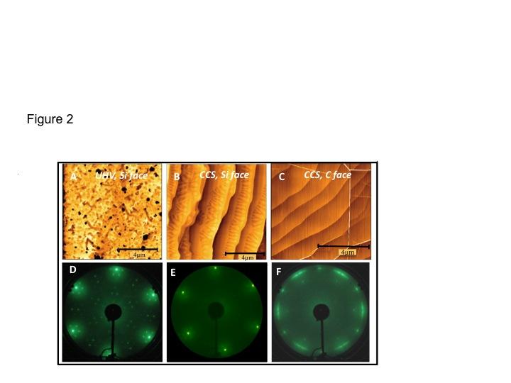
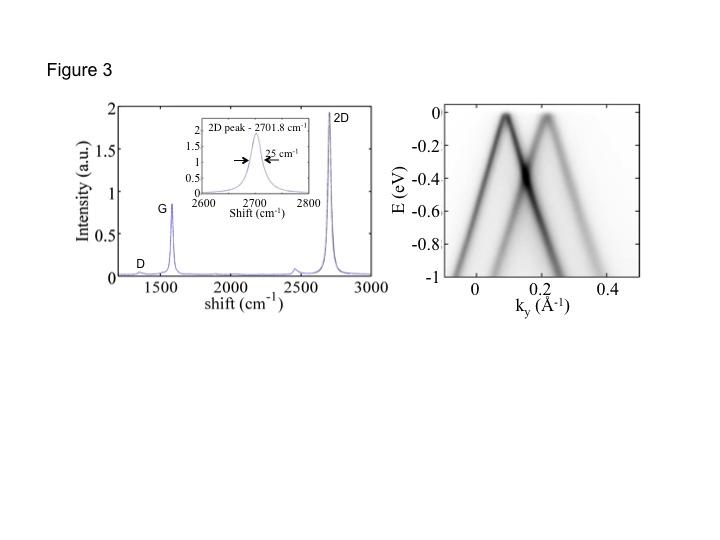
5 Van Bommel also observed that UHV grown graphene on the C-face is both rotationally disordered and defective. 2 However, C-face graphene grown by the CCS method shows rotational order, consisting primary of two principle rotational orientations (Fig. 2F), in contrast to the single orientation in Bernal stacked graphene and Si-face FLG (Fig. 2D). While the exact structure is not known, it is consistent with a stacking where every other layer is aligned within ±~7 degrees of the SiC <21-30> direction and separated by layers rotated by 30 o with respect to the <21-30> direction (Bernal stacked layers make up no more than 15% of the film and are considered stacking faults in this structure). 25 An important consequence of this stacking is that each graphene layer in the stack has the same electronic structure as an isolated graphene sheet and therefore behaves as if it is electronically decoupled from its neighbor. Therefore, C-face multilayers produced by the CCS method are multilayer epitaxial graphene (MEG) 8, 21 and not thin graphite (or FLG). This important property has been confirmed by a variety of probes. For instance the Raman spectrum of the ~100 layer MEG sample of Fig. 3 shows the characteristic G and single Lorentzian 2D peaks of single layer graphene. More specifically, ARPES was used to directly image the linear graphene band structure 20 [see Fig. 2]. In addition, optical transitions between Landau levels in MEG have been observed even at room temperature in low magnetic fields, indicating very weak electron phonon coupling and room temperature mobilities exceed 250,000 cm 2 V -1 s -1 for interior MEG layers 14. These features are clearly important for graphene science. Recent low temperature high magnetic field scanning probe investigations have directly imaged the quantum Hall states in MEG 16. This work also demonstrated that MEG layers are atomically flat (with 50 pm height variations) between substrate steps (that can be up to 50!m apart). An important property of both varieties of EG produced by the CCS method, is that the graphene layers are continuous over substrate steps; the morphology is likened to a carpet that is draped over the SiC surface 8. In fact scanning tunneling microscopy has not revealed a break in the top graphene layer. Hence, at least the top MEG layer covers the entire surface of a macroscopic SiC wafer. The graphene/sic interface on the Si-face is well understood and is defined by a nonconducting carbon rich buffer layer with a 6"3x6"3 structure that causes a corrugation between Å of the first graphene layer. 26, 1 The C-face interface is less well understood. Surface x-ray diffraction indicates that it is also carbon rich with a density close to diamond, while LEED from the thinnest C-face films (discussed below) reveals only a (1x1) pattern. The interface is found to be well defined and flat, consistent with a carbon rich layer at the interface that is tightly bound to the underlying SiC. 26 On both faces, the graphene/sic interface is charged, inducing a negative charge density n gr $ 5x cm -2 on the first graphene layer. ARPES and transport measurements show that this layer (C-face) or the layer just above it (Si-face) in CCS produced epitaxial graphene has the characteristic linear graphene dispersion and high mobility (graphene ribbon mobilities are cm 2 V -1 s -1 for the Si-face and
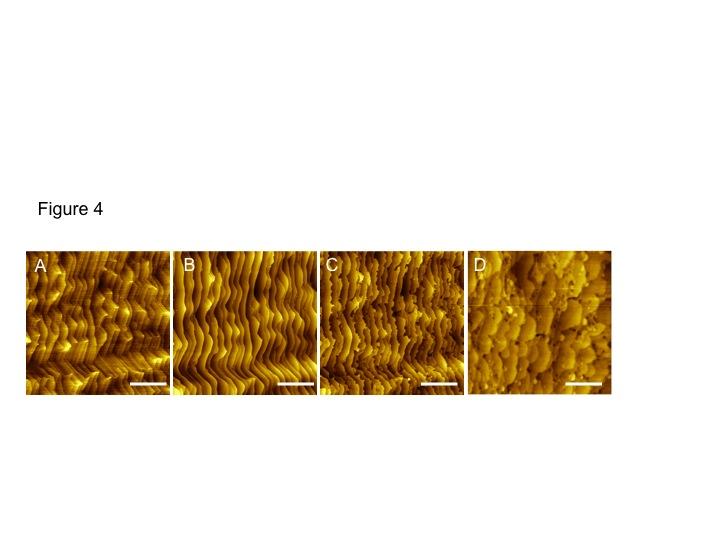
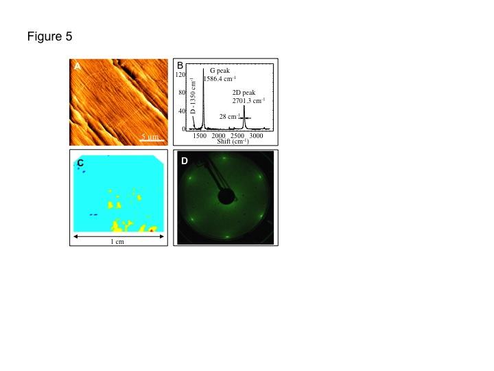
6 10,000-30,000 cm 2 V -1 s -1 for the C-face) 8. The interior layers in MEG are essentially neutral (a screening length of about 1 layer has been measured 27, 28 ). Bernal stacking of graphene layers on the Si-face may explain its low mobilities (compared with the C-face). This may be caused by a graphite bilayer gap that develops from an embryonic second layers that grows at step edges under a completed top graphene layer 13. Since the local bi-layer electronic structure is a significant perturbation to the graphene electronic structure, scattering there will be important. In contrast, because of the electronic decoupling, this scattering mechanism is likely to be suppressed in C-face graphene. The scattering from partially formed layers at the interface is therefore less important for C-face graphene compared with Si-face, explaining the observed large mobility differences. Although electronic scattering mechanisms in graphene are not well understood, it is expected that interface disorder is a significant factor in epitaxial graphene. Interface passivation and annealing processes are being developed to further increase mobilities 29. Applications of the CCS method Large area graphene growth The CCS method is routinely used to cover the entire surface of an on-axis or off-axis cut silicon carbide chips (4H or 6H, Si-face or C-face) with a graphene monolayer or multilayer. These chips are used to measure EG properties or as a starting material for graphene device structures. The various stages of the graphitzation process of a 20!m x 20!m region of a 6H Siface chip are demonstrated in Fig. 4. The hydrogen-etched surface (Fig. 3A) exhibits characteristic half- unit cell silicon carbide steps (0.8 nm) that result from the miscut. The chip was subsequently heated to several temperatures (Fig. 4B-D). At 1300 C, the steps become rounded and at 1400 C, they roughen. The roughing is accompanied by the formation of the buffer layer as verified in LEED and observed to occur at T=1080 C in UHV grown epitaxial graphene. 30 Note that the graphitization temperature increases by ~300 C in the CCS method compared to the UHV method is consistent with the kinetic model of the CCS process. At 1520 C, a high-quality graphene monolayer forms on the C-face in about 20 min (Fig. 5A). In contrast, a defective monolayer forms in a few minutes at 1250 C in UHV 31. It should be noted that AFM images gives the illusion of significant substrate roughness. However, the typical step height is about 1 nm that is about 1/1000 of a typical terrace width. Moreover, the graphene mobilities are high (typically >10,000 cm 2/ Vs on the C-face), even for monolayers 15. Hence, the substrate steps (at least on the C-face) appear not to be a significant source of scattering. Figure 5 shows a 1 cm x 1cm C-face 4H chip that was CCS graphitized. The C-face was graphitized for 10 min at 1550 C to produce an essentially uniform graphene monolayer over the entire surface as verified in ellipsometry measurements (Fig. 5C) (ellipsometer spot size 250!m x 250!m). LEED shows a single set of diffraction
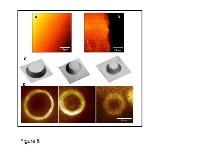
7 spots, consistent with a single graphene layer, oriented 30 o with respect to the SiC lattice (cf Fig 5D). Raman spectroscopy shows characteristics of defect free thin graphene: a narrow 2D peak single Lorentzian centered at 2701cm -1, (FWHM = 28 cm -1 ) and no significant D peak indicating high quality graphene (Fig. 5B). The 2D and G peaks are blue shifted compared with exfoliated graphene flakes on SiO 2 (by ~6cm -1 and 20cm -1 respectively), but the shift is smaller than for epitaxial graphene on the Si-face. The peaks position does not vary significantly with the number of layers, and a single Lorentzian 2D peak is primarily observed on very thick MEG films as a result of the electronic decoupling. The blue shift observed in Si face graphene is attributed to strain due to a differential thermal contraction upon cooling between the SiC substrate and the graphene 32. The small shift observed here indicates a reduced strain in C-face grown mono and multilayers. Sample to sample variability is observed in the magnitude of the shifts and peak intensities. The expected attenuation of the SiC signal correlates well with sample thickness, allowing a crude sample thickness measurement from Raman data with a precision of about 2-3 layers. Atomic force microscopy (AFM) images like Fig. 5A show the typical pleat structure of the C-face epitaxial graphene layer (pleats are not typically seen on Si-face graphene). The pleats (also called puckers, ridges, creases, rumples, ripples and folds) are typically 1-10 nm high, are typically spaced 3-10!m apart and are thought to result from the differential expansion of the silicon carbide and graphene and the very weak coupling of the graphene to the substrate. Room temperature van der Pauw transport measurements over the 1 cm x 1cm area give a Hall mobility of 2000 cm 2 V -1 s -1. We find that transport measurements over cm size scales typically give significantly lower values than measurements of micron sized Hall bars, which may be related to residual inhomogeneities over macroscopic length scales. In contrast, STM studies show that graphene structure is continuous over the pleats and transport measurement show that pleats do not significantly affect the transport, in fact high mobility monolayer graphene Hall bars (!~20,000 cm 2 V -1 s -1 ) with many pleats show a well-developed quantum Hall effect and no indication of non-uniform transport 15. Large area graphene multilayers are grown both on the C-face and the Si-face by increasing the annealing times and the temperatures. For large area C-face growth, temperatures in the range of C are preferred because at these reduced temperatures, step bunching is reduced so that large substrate steps are avoided. Note however, that over macroscopic distances, the unavoidable miscut of a nominally flat SiC crystal (of order 0.05 ) always results in substrate steps. Growing graphene on mesas One way to control and to eliminate substrate steps in defined regions of the silicon carbide substrate, is to etch mesas on the surface. The subsequent heat treatment will cause the substrate steps to flow and bunch at the mesa boundaries and ultimately produce step-free SiC surfaces.
8 This process relates to earlier research that demonstrated step-free mesas in heteroepitaxial SiC step-flow growth on vicinal SiC, where step pinning occurs at the step edges 33. The near equilibrium growth with correspondingly higher kinetics in the CCS process goes beyond step flow growth to approach near equilibrium crystal shapes with essentially atomically flat surfaces. Subsequent graphitization produces atomically flat graphene (except for the pleats). Growth on mesas is demonstrated on hexagonal and square mesas, 2 micron high, that were lithographically etched on the C-face of a 4H-SiC chip. The samples were heated to 1250 C for 20 min and subsequently to 1600 C for 10 min. Mesas smaller than 20!m generally became flat and the edges slope at a 57 deg angle from the vertical. While substrate steps are still observed on these surfaces, their densities are at least a factor of 10 smaller than the on the original hydrogen etched SiC surface. We have further found that graphene formation inhibits step bunching. Therefore the mesas were produced by annealing the structures twice and graphene layer was etched away (using an oxygen plasma etch) between the annealing steps. Figure 6 B shows part of a 100!m x 100!m mesa, that corresponds to essentially a single SiC terrace (cf. Fig. 5 A). Conditions are currently sought under which the graphene growth is so slow that the SiC surfaces anneal to their equilibrium shapes before they graphitize. In that case mesa flattening and graphene growth can be accomplished in one step. Structured graphene growth Extended graphene sheets are important for basic research. However, essentially all electronic applications require graphene to be patterned. In fact, graphene electronics relies on the possibly to interconnect nanoscopic graphene structures. An extended graphene sheet is a gapless semimetal but a graphene ribbon is expected to develop a bandgap &E$1eV/W, where W is the width of the ribbon in nm 34, 35. Graphene ribbons can be patterned using standard microelectronics lithography methods 36. In these methods, an extended graphene sheet is coated with an electron-beam resist material (for example, PMMA) that is patterned by e-beam lithography. After development of the resist, the graphene is oxygen ion-etched to produce the desired structures. It is clear that the lithography steps themselves are destructive and produce non-ideal edges and poorly defined structures at the nanoscale. This contributes to significantly reduced mobilities and spurious electronic localization effects 35 In fact the mobility reduction in conventionally patterned structures is so severe that the nanoelectronics applications potential of graphene has been called into question. It is clearly advantageous to avoid processing steps that involve cutting the graphene. A nuanced approach that avoids nanolithography of the graphene is clearly desired. A very promising method is to grow graphene on structured silicon carbide. In this method, the ungraphitized Si-face (0001) of silicon carbide is lithographically patterned in the usual way using a resist coating. The exposed SiC areas are then plasma etched using SF 6 or CF 4 so to produce depressions of well-defined depths ranging from a few nm to microns as controlled by the intensity and duration of the plasma etching procedure. The sample is finally annealed and graphitized by the CCS method at temperatures typically in the range of 1550 C to 1650 C.
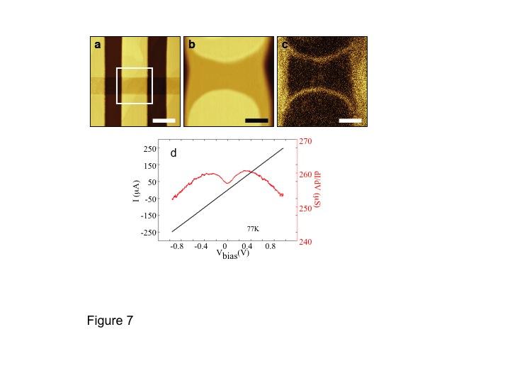
9 In this process, the sidewalls of the etched structures crystallize, typically along the (1-10n) direction, n=8 for 4H SiC and n=12 for 6H SiC. Consequently a circular etched mesa with a diameter of 1!m will crystallize into hexagons (Fig. 6c) where the sidewall slopes are about 62 deg from the vertical. The graphitization rates of the (1-10n) sidewalls are similar to the graphitization rates of the (000-1) surfaces (i.e. the C-face) of SiC. Because these rates are much greater than the graphitization rates of the Si-face horizontal surfaces, only the sidewalls and not the (0001) flat surfaces are graphitized. Consequently, this graphitization method can be controlled to produce monolayer graphene on the sidewalls while graphene on the horizontal (0001) surfaces are sub-monolayer and non-conducting. This has been verified by Raman spectroscopy and by transport measurements. Along the same lines, graphitization on natural (non pre-etched) vicinal steps of SiC on-axis or off-axis (4 degree or 8 degree from (0001)) produce arrays of narrow ribbons. Significant step bunching precedes the graphitization to produce step heights on the order of 10 nm with corresponding ribbon widths. The process has been applied to more complex structures as shown in Fig. 7A-C, where a two vertical 400 nm deep trenches are crossed with a 15 nm deep, 1!m wide depression. The structure is annealed and graphitized using the CCS method. Annealing causes the observed rounding of the previously straight sidewalls and graphitization produces a 40 nm graphene sidewall ribbon as revealed by electrostatic force microscopy. The increased width compared with the sidewall width is caused by recrystallization of the vertical sidewalls (initially exposing a face) to (1-10n) with a reduced slope (23 deg from horizontal for n =10) to produce wider ribbons. The narrow ribbons are seamlessly connected to wide ribbons that were formed on the sidewalls of the deep trench as revealed in the electrostatic force micrograph (Fig. 7C). Transport measurements demonstrate the continuity of the sidewall ribbons. The resistivity of sidewall ribbons is about 100 _ per square, which is comparable to measurements on doped two dimensional epitaxial graphene sheets (n doping on the order of /cm 2 is typically observed). These resitivities are orders of magnitude smaller than observed in lithographically patterned ribbons of comparable width, indicating that the sidewall graphitization method produces ribbons with smoother edges. Moreover, there is no evidence for Coulomb blockade effects that result from edge roughness in exfoliated graphene ribbons 37. In fact, recent measurements of gated sidewall ribbons between 20 and 40 nm wide and from 1 to 2!m long indicate that they are ballistic, resembling carbon nanotubes in that respect. In fact, there is no indication of a bandgap in these ribbons (these results will be published elsewhere). These examples show that sidewall graphitization is an effective and simple method to produce interconnected nanoscopic graphene ribbons and other graphene nanostructures, without resorting to nanolithographic methods.
10 Summary and conclusion The near equilibrium, confinement controlled sublimation method to produce epitaxial graphene (mono and multi) layers on silicon carbide has been demonstrated to be a versatile method to produce high quality uniform graphene layers on both the Si-face and the C-face of single crystal silicon carbide. It provides control of the silicon vapor density and assures that the density is constant over the surface and near thermodynamic equilibrium, which is essential for uniform growth. The method allows good control of the graphitization temperatures, which is important, since growth at low temperatures (as in the case of sublimation in unconfined ultra-high vacuum) produces defective graphene layers. The CCS method allows further control of the graphitization rates by introducing inert gasses, which can essentially inhibit the graphene growth even at temperatures exceeding 1600 C. This is important if the graphitization is preceded by an annealing step of the silicon carbide surface itself for example to anneal (or recrystallize) a structured silicon carbide surface. Graphene electronics imposes great demands on the material and material processing. It should be clear that the realization of graphene-based electronics requires all of these conditions to be met. The CCS method is an important step in the production of high quality graphene both in single layers and multilayers. Sidewall graphitization by the CCS method has recently been advanced to the point that narrow ballistic graphene ribbons can be made. This is an important development that overcomes the edge roughness, which is the most serious lithography problem. Hence, graphene ribbons are approaching the electronic quality of carbon nanotubes. Furthermore, beyond graphene growth, great advances have been made in producing effective top gate structures that do not introduce additional scattering. Despite all these advances, graphene based electronics has not yet been realized. However given progress in epitaxial graphene on silicon carbide, the prospects are encouraging. Acknowledgements The authors thank the W. M Keck foundation, the National Science Foundation (DMR ), the Air Force Office of Scientific Research for financial support and the Partner University Fund for travel grant. References 1. Boehm, H., Clauss, A., Hofmann, U & Fischer, G. Dunnste Kohlenstof-Folien. Z Fur Naturforschung B 17, 150 (1962). 2. Van Bommel, A., Crombeen, J. & van Tooren, A. LEED and Auger-electron observations of SiC (0001) surface. Surface Science 48, (1975). 3. Gall, N.R., RutKov, E.V. & Tontegode, A.Y. Two dimensional graphite films on metals and their intercalation. Int. J. of Mod. Phys. B 11, (1997).
11 4. de Heer W.A., Berger, C., First, P.N. United States Patent US , filed June 2003, issued 2006; de Heer, W.A. Early Development of Graphene Electronics. (2009) at < 5. Berger, C. et al. Ultrathin epitaxial graphite: 2D electron gas properties and a route toward graphene-based nanoelectronics. J. Phys. Chem. B 108, (2004). 6. Forbeaux, I., Themlin, J.M. & Debever, J.M. Heteroepitaxial graphite on 6H- SiC(0001): Interface formation through conduction-band electronic structure. Phys. Rev. B 58, (1998). 7. Novoselov, K.S. et al. Electric Field Effect in Atomically Thin Carbon Films. Science 306, (2004). 8. de Heer, W. et al. Epitaxial graphene. Solid State. Com. 143, (2007). 9. Ando, T., Fowler, A.B. & Stern, F. Electronic properties of two-dimensional systems. Reviews of Modern Physics 54, (1982). 10. McEuen, P.L., Fuhrer, M.S. & Park, H.K. Single-walled carbon nanotube electronics. IEEE Transactions on Nanotechnology 1, (2002). 11. Soule, D. & McClure, J. Band Structure And Transport Properties Of Single- Crystal Graphite. J. Phys. Chem. of Solids 8, (1959). 12. Tromp, R. & Hannon, J. Thermodynamics and kinetics of graphene growth on SiC(0001). Phys. Rev. Lett. 102, (2009). 13. Emtsev, K. et al. Towards wafer-size graphene layers by atmospheric pressure graphitization of silicon carbide. Nature Mat. 8, (2009). 14. Orlita, M. et al. Approaching the Dirac Point in High-Mobility Multilayer Epitaxial Graphene. Phys. Rev. Lett 101, (2008). 15. Wu, X. et al. Half integer quantum Hall effect in high mobility single layer epitaxial graphene. App. Phys. Lett. 95, (2009). 16. Miller, D.L. et al. Observing the Quantization of Zero Mass Carriers in Graphene. Science 324, (2009). 17. Song, Y. et al. High-resolution tunnelling spectroscopy of a graphene quartet. Nature 467, (2010). 18. Sprinkle, M. et al. Scalable templated growth of graphene nanoribbons on SiC. Nature Nanotech 5, (2010). 19. Berger, C. et al. Electronic confinement and coherence in patterned epitaxial graphene. Science 312, 1191 (2006) 20. Sprinkle, M. et al. First direct observation of a nearly ideal graphene band structure. Phys. Rev. Lett. 103, 4 (2009). 21. Hass, J. et al. Why multilayer graphene on 4H-SiC(000$1$) behaves like a single sheet of graphene. Phys. Rev. Lett. 100, (2008). 22. Lilov, S. Study of the Equilibrium Processes In The Gas-Phase During Silicon- Carbide Sublimation. Mat. Science and Engineering B- 21, (1993). 23. Hoffman, D., Singh, B. & Thomas, I.J.H. Handbook of Vacuum Science and Technology. (Academic Press: 1998). 24. Zhou, S.Y. et al. Substrate-induced bandgap opening in epitaxial graphene. Nature Materials 6, (2007).
12 25. Sprinkle, M. et al. Multilayer epitaxial graphene grown on the SiC (000-1) surface; structure and electronic properties. J. Phys. D 43, (2010). 26. Hass, J., Millan-Otoya, J., First, P. & Conrad, E. Interface structure of epitaxial graphene grown on 4H-SiC(0001). Phys. Rev. B 78, (2008). 27. Sun, D. et al. Spectroscopic Measurement of Interlayer Screening in Multilayer Epitaxial Graphene. Phys. Rev. Lett. 104, (2009). 28. Sun, D. et al. Ultrafast Relaxation of Excited Dirac Fermions in Epitaxial Graphene Using Optical Differential Transmission Spectroscopy. Phys. Rev. Lett. 101, (2008). 29. Riedl, C., Coletti, C., Iwasaki, T., Zakharov, A.A. & Starke, U. Quasi-free Standing Epitaxial Graphene on SiC by Hydrogen Intercalation. Phys. Rev. Lett. 103, (2009). 30. Emtsev, K., Speck, F., Seyller, T., Ley, L. & Riley, J. Interaction, growth, and ordering of epitaxial graphene on SiC{0001} surfaces: A comparative photoelectron spectroscopy study. Phys. Rev. B 77, (2008). 31. Mallet, P. et al. Electron states of mono- and bilayer graphene on SiC probed by scanning-tunneling microscopy. Phys. Rev. B 76, (2007). 32. Rohrl, J. et al. Raman spectra of epitaxial graphene on SiC(0001). Appl. Phys. Lett. 92, (2008). 33. Powell, J. et al. Growth of step-free surfaces on device-size (0001)SiC mesas. Appl. Phys. Lett. 77, (2000). 34. Nakada, K., Fujita, M., Dresselhaus, G. & Dresselhaus, M.S. Edge state in graphene ribbons: Nanometer size effect and edge shape dependence. Phys. Rev. B 54, (1996). 35. Han, M.Y., Ozyilmaz, B., Zhang, Y. & Kim, P. Energy Band-Gap Engineering of Graphene Nanoribbons. Phys. Rev. Lett. 98, (2007). 36. Li, X. et al. Top- and side-gated epitaxial graphene field effect transistors. Phys. Stat. Solid. 207, (2010). 37. Ozyilmaz, B., Jarillo-Herrero, P., Efetov, D. & Kim, P. Electronic transport in locally gated graphene nanoconstrictions. Appl. Phys. Lett. 91, (2007). Figure Captions Figure 1: The Confinement Controlled Sublimation method. (A) SiC wafer in UHV: sublimed silicon is not confined, causing rapid, out of equilibrium graphene growth. (B) The CCS method: sublimed Si gas is confined in a graphite enclosure so that growth occurs in near thermodynamic equilibrium. Growth rate is controlled by the enclosure aperture (leak), and the background gas pressure. (C) Photograph of the induction furnace. (D) under CCS conditions few layer graphite (FLG, from 1 to 10 layers) grows on the Si terminated face, and multilayer epitaxial graphene (MEG, from 1 to 100 layers) grows on the C terminated face.
13 Figure 2: Comparison of UHV and CCS grown epitaxial graphene. (A-C) AFM images and (D- F) LEED patterns. (A) UHV grown monolayer on the Si-face. (B) CCS monolayer grown on Si-face. (C) MEG on C face; note that layers drape over the substrate steps (white lines are pleats in the MEG layer). (D) LEED pattern of CCS grown Si-face graphene monolayer (bright spots due to graphene) showing typical surface reconstruction features. (E) LEED image of CCS grown C-face monolayer; (F) LEED image of CCS grown C-face multilayer (MEG), showing characteristic arcs due to the rotational stacking. Figure 3: Raman and ARPES spectroscopy of MEG (left and right panels, resp.). Raman spectrum shows the characteristic G and 2D graphene peaks. The 2D peak of this ~100 layer MEG sample fits a single Lorentzian of full width 25cm -1, centered at cm -1. A weak D peak can be discerned. ARPES data from the top three layers of a 10 layer sample around k y =0 (i.e., the Dirac point). Two unperturbed cones are observed showing that the layers are electronically decoupled: the slope is v F =1x10 6 m/s, as expected for isolated graphene, and the Fermi level is with 20 mev from the Dirac point. For details, see Ref. 20. Figure 4: AFM images showing the evolution of the surface of the 6H Si-face upon annealing. (A) initial surface after hydrogen etching showing half-unit cell steps (0.8 nm) resulting from the miscut; (B) After CCS annealing at 1300 C: substrate steps become rounded, (C) annealing at 1400C; the steps roughen, and (D) 1500 C: formation of a graphene layer. The scale bar is 5!m. Figure 5: Single layer graphene grown on a 1cm x 1cm 4H-SiC chip on the C-face. (A) AFM image showing a graphene coated stepped SiC surface; note the continuous pleats running across large regions of the surface. (B) The Raman spectrum (after SiC background subtraction); the 2D peak consists of single Lorentzian (full width =28 cm -1 ); the disorder induced D peak is absent. (C) Ellipsometry shows graphene uniformity (color scale light blue: 1 layer, yellow: 2 layers, red: 3 layers, dark blue: no graphene; beam size : 250!m x 250!m). (D) LEED pattern of the monolayer. Figure 6: Examples of template grown graphene structures etched on the (0001) face. (A) 4H- SiC hydrogen-etched surface with a regular step structure. (B) Flat step-free graphitized mesa with MEG pleats (C) circular mesa etched on Si-face; the hexagonal
14 shape results from the annealing at 1550 C showing preference for the (1-10n) crystal surfaces (n depends on the step height and ranges from 2, for nm steps to about 10 for!m steps). (D) Electrostatic force microscopy image after CCS annealing; graphene (light) grows on the mesa sidewalls but not on the horizontal (0001) surfaces. Figure 7: Templated CCS sidewall graphene ribbons. (a) AFM image of two 1!m deep trenches (brown) etched in SiC Si-face (scale bars are 1!m). The trenches are connected by a 10 nm deep trench (light brown). (b) After annealing, the initially straight trench walls becomes rounded, indicating significant SiC mass flow. (c) EFM shows that 20 nm graphene graphene ribbons have grown on the trench sidewalls (verified in Raman spectroscopy). The wide graphene ribbons concurrently grown on deep!m high sidewalls serve as current leads and voltage probes. (d) I-V characteristics of the two 20 nm wide, 1.5!m long ribbons in parallel. The resistance corresponds to 8 k% per ribbon (corresponding to about 100 %/square) and exhibits a weak zero bias anomaly.
15
16
17
18
19
20
21
Large area and structured epitaxial graphene produced by confinement controlled sublimation of silicon carbide
 Large area and structured epitaxial graphene produced by confinement controlled sublimation of silicon carbide Walt A. de Heer a,1, Claire Berger a,b, Ming Ruan a, Mike Sprinkle a, Xuebin Li a, Yike Hu
Exceptional ballistic transport in epigraphene. Walt de Heer Georgia Institute of Technology
 Exceptional ballistic transport in epigraphene Walt de Heer Georgia Institute of Technology Program Objective First formulated in 2001 and patented in 2003, our objective is to develop nanoelectronics
Optimizing Graphene Morphology on SiC(0001)
") Optimizing Graphene Morphology on SiC(0001) James B. Hannon Rudolf M. Tromp Graphene sheets Graphene sheets can be formed into 0D,1D, 2D, and 3D structures Chemically inert Intrinsically high carrier mobility
Optimizing Graphene Morphology on SiC(0001) James B. Hannon Rudolf M. Tromp Graphene sheets Graphene sheets can be formed into 0D,1D, 2D, and 3D structures Chemically inert Intrinsically high carrier mobility
SUPPLEMENTARY INFORMATION
 SUPPLEMENTARY INFORMATION Towards wafer-size graphene layers by atmospheric pressure graphitization of silicon carbide Supporting online material Konstantin V. Emtsev 1, Aaron Bostwick 2, Karsten Horn
Graphene. Tianyu Ye November 30th, 2011
 Graphene Tianyu Ye November 30th, 2011 Outline What is graphene? How to make graphene? (Exfoliation, Epitaxial, CVD) Is it graphene? (Identification methods) Transport properties; Other properties; Applications;
Surface atoms/molecules of a material act as an interface to its surrounding environment;
 1 Chapter 1 Thesis Overview Surface atoms/molecules of a material act as an interface to its surrounding environment; their properties are often complicated by external adsorbates/species on the surface
Graphene: Plane and Simple Electrical Metrology?
 Graphene: Plane and Simple Electrical Metrology? R. E. Elmquist, F. L. Hernandez-Marquez, M. Real, T. Shen, D. B. Newell, C. J. Jacob, and G. R. Jones, Jr. National Institute of Standards and Technology,
Yugang Sun Center for Nanoscale Materials, Argonne National Laboratory, Argonne, IL 60439
 Morphology of Graphene on SiC( 000 1 ) Surfaces Luxmi, P. J. Fisher, N. Srivastava, and R. M. Feenstra Dept. Physics, Carnegie Mellon University, Pittsburgh, PA 15213 Yugang Sun Center for Nanoscale Materials,
Hydrogenated Graphene
 Hydrogenated Graphene Stefan Heun NEST, Istituto Nanoscienze-CNR and Scuola Normale Superiore Pisa, Italy Outline Epitaxial Graphene Hydrogen Chemisorbed on Graphene Hydrogen-Intercalated Graphene Outline
SUPPLEMENTARY INFORMATION
 SUPPLEMENTARY INFORMATION Facile Synthesis of High Quality Graphene Nanoribbons Liying Jiao, Xinran Wang, Georgi Diankov, Hailiang Wang & Hongjie Dai* Supplementary Information 1. Photograph of graphene
TRANSVERSE SPIN TRANSPORT IN GRAPHENE
 International Journal of Modern Physics B Vol. 23, Nos. 12 & 13 (2009) 2641 2646 World Scientific Publishing Company TRANSVERSE SPIN TRANSPORT IN GRAPHENE TARIQ M. G. MOHIUDDIN, A. A. ZHUKOV, D. C. ELIAS,
Supplementary information
 Supplementary information Supplementary Figure S1STM images of four GNBs and their corresponding STS spectra. a-d, STM images of four GNBs are shown in the left side. The experimental STS data with respective
.Fritjaf Capra, The Tao of Physics
 Probing inside the atom and investigating its structure, science transcended the limits of our sensory imagination. From this point on, it could no longer rely with absolute certainty on logic and common
Graphene films on silicon carbide (SiC) wafers supplied by Nitride Crystals, Inc.
 wafers supplied by Nitride Crystals, Inc.") 9702 Gayton Road, Suite 320, Richmond, VA 23238, USA Phone: +1 (804) 709-6696 info@nitride-crystals.com www.nitride-crystals.com Graphene films on silicon carbide (SiC) wafers supplied by Nitride Crystals,
9702 Gayton Road, Suite 320, Richmond, VA 23238, USA Phone: +1 (804) 709-6696 info@nitride-crystals.com www.nitride-crystals.com Graphene films on silicon carbide (SiC) wafers supplied by Nitride Crystals,
Epitaxial graphene on SiC(0001): More than just honeycombs. Y. Qi, S. H. Rhim, G. F. Sun, M. Weinert, and L. Li*
: More than just honeycombs. Y. Qi, S. H. Rhim, G. F. Sun, M. Weinert, and L. Li*") Epitaxial graphene on SiC(0001): More than just honeycombs Y. Qi, S. H. Rhim, G. F. Sun, M. Weinert, and L. Li* Department of Physics and Laboratory for Surface Studies University of Wisconsin, Milwaukee,
Epitaxial graphene on SiC(0001): More than just honeycombs Y. Qi, S. H. Rhim, G. F. Sun, M. Weinert, and L. Li* Department of Physics and Laboratory for Surface Studies University of Wisconsin, Milwaukee,
Graphene Novel Material for Nanoelectronics
 Graphene Novel Material for Nanoelectronics Shintaro Sato Naoki Harada Daiyu Kondo Mari Ohfuchi (Manuscript received May 12, 2009) Graphene is a flat monolayer of carbon atoms with a two-dimensional honeycomb
A. Optimizing the growth conditions of large-scale graphene films
 1 A. Optimizing the growth conditions of large-scale graphene films Figure S1. Optical microscope images of graphene films transferred on 300 nm SiO 2 /Si substrates. a, Images of the graphene films grown
Surface Science 604 (2010) Contents lists available at ScienceDirect. Surface Science. journal homepage:
 Contents lists available at ScienceDirect. Surface Science. journal homepage:") Surface Science 604 (2010) 84 88 Contents lists available at ScienceDirect Surface Science journal homepage: www.elsevier.com/locate/susc Signatures of epitaxial graphene grown on Si-terminated 6H-SiC
Surface Science 604 (2010) 84 88 Contents lists available at ScienceDirect Surface Science journal homepage: www.elsevier.com/locate/susc Signatures of epitaxial graphene grown on Si-terminated 6H-SiC
Decoupling Graphene from SiC(0001) via Oxidation
 via Oxidation") Decoupling Graphene from SiC(0001) via Oxidation S. Oida, F.R. McFeely, J.B. Hannon, R.M. Tromp, M. Copel, Z. Chen, Y. Sun, D.B. Farmer and J. Yurkas 1 IBM Research Division, T.J. Watson Research Center,
Decoupling Graphene from SiC(0001) via Oxidation S. Oida, F.R. McFeely, J.B. Hannon, R.M. Tromp, M. Copel, Z. Chen, Y. Sun, D.B. Farmer and J. Yurkas 1 IBM Research Division, T.J. Watson Research Center,
Carbon based Nanoscale Electronics
 Carbon based Nanoscale Electronics 09 02 200802 2008 ME class Outline driving force for the carbon nanomaterial electronic properties of fullerene exploration of electronic carbon nanotube gold rush of
SiC Graphene Suitable For Quantum Hall Resistance Metrology.
 SiC Graphene Suitable For Quantum Hall Resistance Metrology. Samuel Lara-Avila 1, Alexei Kalaboukhov 1, Sara Paolillo, Mikael Syväjärvi 3, Rositza Yakimova 3, Vladimir Fal'ko 4, Alexander Tzalenchuk 5,
Supplementary Information
 Supplementary Information Supplementary Figure 1. fabrication. A schematic of the experimental setup used for graphene Supplementary Figure 2. Emission spectrum of the plasma: Negative peaks indicate an
Scalable templated growth of graphene nanoribbons on SiC
 Scalable templated growth of graphene nanoribbons on SiC Mike Sprinkle, Ming Ruan, Yike Hu, John H. Hankinson, Miguel Rubio-Roy, Baiqian Zhang, Xiaosong Wu, Claire Berger, Walt. A. De Heer To cite this
Tutorial T5 Will Carbon Replace Silicon? The future of graphitic electronics.
 Tutorial T5 Will Carbon Replace Silicon? The future of graphitic electronics. 1:30-2:20 Jim Meindl Nanoelectronics in Retrospect and Prospect 2:20-3:10 Millie Dresselhaus From Graphene to Graphite to Nanotubes
Supplementary Figure 1 Detailed illustration on the fabrication process of templatestripped
 Supplementary Figure 1 Detailed illustration on the fabrication process of templatestripped gold substrate. (a) Spin coating of hydrogen silsesquioxane (HSQ) resist onto the silicon substrate with a thickness
XPS Depth Profiling of Epitaxial Graphene Intercalated with FeCl 3
 XPS Depth Profiling of Epitaxial Graphene Intercalated with FeCl 3 Mahdi Ibrahim Maynard H. Jackson High School Atlanta, GA. Faculty Advisor: Dr. Kristin Shepperd Research Group: Prof. Edward Conrad School
Supplementary Figure 1 Experimental setup for crystal growth. Schematic drawing of the experimental setup for C 8 -BTBT crystal growth.
 Supplementary Figure 1 Experimental setup for crystal growth. Schematic drawing of the experimental setup for C 8 -BTBT crystal growth. Supplementary Figure 2 AFM study of the C 8 -BTBT crystal growth
Growing Graphene on Semiconductors
 Growing Graphene on Semiconductors edited by Nunzio Motta Francesca Iacopi Camilla Coletti Growing Graphene on Semiconductors Growing Graphene on Semiconductors edited by Nunzio Motta Francesca Iacopi
Intrinsic Electronic Transport Properties of High. Information
 Intrinsic Electronic Transport Properties of High Quality and MoS 2 : Supporting Information Britton W. H. Baugher, Hugh O. H. Churchill, Yafang Yang, and Pablo Jarillo-Herrero Department of Physics, Massachusetts
Wide-gap Semiconducting Graphene from Nitrogen-seeded SiC
 Wide-gap Semiconducting Graphene from Nitrogen-seeded SiC F. Wang, 1 G. Liu, 2 S. Rothwell, 3 M. Nevius, 1 A. Tejeda, 4, 5 A. Taleb-Ibrahimi, 6 L.C. Feldman, 2 P.I. Cohen, 3 and E.H. Conrad 1 1 School
Solid Surfaces, Interfaces and Thin Films
 Hans Lüth Solid Surfaces, Interfaces and Thin Films Fifth Edition With 427 Figures.2e Springer Contents 1 Surface and Interface Physics: Its Definition and Importance... 1 Panel I: Ultrahigh Vacuum (UHV)
Magnetotransport in high mobility epitaxial graphene
 Early View publication on www.interscience.wiley.com (issue and page numbers not yet assigned; citable using Digital Object Identifier DOI) Original phys. stat. sol. (a), 1 5 (2007) / DOI 10.1002/pssa.200675352
1. Nanotechnology & nanomaterials -- Functional nanomaterials enabled by nanotechnologies.
 Novel Nano-Engineered Semiconductors for Possible Photon Sources and Detectors NAI-CHANG YEH Department of Physics, California Institute of Technology 1. Nanotechnology & nanomaterials -- Functional nanomaterials
Frictional characteristics of exfoliated and epitaxial graphene
 Frictional characteristics of exfoliated and epitaxial graphene Young Jun Shin a,b, Ryan Stromberg c, Rick Nay c, Han Huang d, Andrew T. S. Wee d, Hyunsoo Yang a,b,*, Charanjit S. Bhatia a a Department
The effect of a SiC cap on the growth of epitaxial graphene on SiC in ultra high vacuum
 CARBON 50 (2012) 3026 3031 Available at www.sciencedirect.com journal homepage: www.elsevier.com/locate/carbon The effect of a SiC cap on the growth of epitaxial graphene on SiC in ultra high vacuum Cem
Supporting Information. by Hexagonal Boron Nitride
 Supporting Information High Velocity Saturation in Graphene Encapsulated by Hexagonal Boron Nitride Megan A. Yamoah 1,2,, Wenmin Yang 1,3, Eric Pop 4,5,6, David Goldhaber-Gordon 1 * 1 Department of Physics,
NiCl2 Solution concentration. Etching Duration. Aspect ratio. Experiment Atmosphere Temperature. Length(µm) Width (nm) Ar:H2=9:1, 150Pa
 Width (nm) Ar:H2=9:1, 150Pa") Experiment Atmosphere Temperature #1 # 2 # 3 # 4 # 5 # 6 # 7 # 8 # 9 # 10 Ar:H2=9:1, 150Pa Ar:H2=9:1, 150Pa Ar:H2=9:1, 150Pa Ar:H2=9:1, 150Pa Ar:H2=9:1, 150Pa Ar:H2=9:1, 150Pa Ar:H2=9:1, 150Pa Ar:H2=9:1,
Experiment Atmosphere Temperature #1 # 2 # 3 # 4 # 5 # 6 # 7 # 8 # 9 # 10 Ar:H2=9:1, 150Pa Ar:H2=9:1, 150Pa Ar:H2=9:1, 150Pa Ar:H2=9:1, 150Pa Ar:H2=9:1, 150Pa Ar:H2=9:1, 150Pa Ar:H2=9:1, 150Pa Ar:H2=9:1,
Analysis of the Formation Conditions for Large Area Epitaxial Graphene on SiC Substrates
 Analysis of the Formation Conditions for Large Area Epitaxial Graphene on SiC Substrates Rositsa Yakimova, Chariya Virojanadara, Daniela Gogova, Mikael Syväjärvi, D. Siche, Krister Larsson and Leif Johansson
GRAPHENE ON THE Si-FACE OF SILICON CARBIDE USER MANUAL
 GRAPHENE ON THE Si-FACE OF SILICON CARBIDE USER MANUAL 1. INTRODUCTION Silicon Carbide (SiC) is a wide band gap semiconductor that exists in different polytypes. The substrate used for the fabrication
arxiv: v1 [cond-mat.mtrl-sci] 3 May 2015
![arxiv: v1 [cond-mat.mtrl-sci] 3 May 2015](/thumbs/94/118238290.jpg "arxiv: v1 [cond-mat.mtrl-sci] 3 May 2015") Semiconducting graphene from highly ordered substrate interactions M.S. Nevius,1 M. Conrad,1 F. Wang,1 A. Celis,2, 3 M.N. Nair,4 A. Taleb-Ibrahimi,4 A. Tejeda,2, 3 and E.H. Conrad1, 1 arxiv:1505.00435v1
Semiconducting graphene from highly ordered substrate interactions M.S. Nevius,1 M. Conrad,1 F. Wang,1 A. Celis,2, 3 M.N. Nair,4 A. Taleb-Ibrahimi,4 A. Tejeda,2, 3 and E.H. Conrad1, 1 arxiv:1505.00435v1
Low Voltage Field Emission SEM (LV FE-SEM): A Promising Imaging Approach for Graphene Samples
: A Promising Imaging Approach for Graphene Samples") Low Voltage Field Emission SEM (LV FE-SEM): A Promising Imaging Approach for Graphene Samples Jining Xie Agilent Technologies May 23 rd, 2012 www.agilent.com/find/nano Outline 1. Introduction 2. Agilent
Low Voltage Field Emission SEM (LV FE-SEM): A Promising Imaging Approach for Graphene Samples Jining Xie Agilent Technologies May 23 rd, 2012 www.agilent.com/find/nano Outline 1. Introduction 2. Agilent
Black phosphorus: A new bandgap tuning knob
 Black phosphorus: A new bandgap tuning knob Rafael Roldán and Andres Castellanos-Gomez Modern electronics rely on devices whose functionality can be adjusted by the end-user with an external knob. A new
Self-Doping Effects in Epitaxially-Grown Graphene. Abstract
 Self-Doping Effects in Epitaxially-Grown Graphene D.A.Siegel, 1,2 S.Y.Zhou, 1,2 F.ElGabaly, 3 A.V.Fedorov, 4 A.K.Schmid, 3 anda.lanzara 1,2 1 Department of Physics, University of California, Berkeley,
Raman Imaging and Electronic Properties of Graphene
 Raman Imaging and Electronic Properties of Graphene F. Molitor, D. Graf, C. Stampfer, T. Ihn, and K. Ensslin Laboratory for Solid State Physics, ETH Zurich, 8093 Zurich, Switzerland ensslin@phys.ethz.ch
Impact of disorder and topology in two dimensional systems at low carrier densities
 Impact of disorder and topology in two dimensional systems at low carrier densities A Thesis Submitted For the Degree of Doctor of Philosophy in the Faculty of Science by Mohammed Ali Aamir Department
An account of our efforts towards air quality monitoring in epitaxial graphene on SiC
 European Network on New Sensing Technologies for Air Pollution Control and Environmental Sustainability - EuNetAir COST Action TD1105 2 nd International Workshop EuNetAir on New Sensing Technologies for
Supplementary information for Tunneling Spectroscopy of Graphene-Boron Nitride Heterostructures
 Supplementary information for Tunneling Spectroscopy of Graphene-Boron Nitride Heterostructures F. Amet, 1 J. R. Williams, 2 A. G. F. Garcia, 2 M. Yankowitz, 2 K.Watanabe, 3 T.Taniguchi, 3 and D. Goldhaber-Gordon
SUPPLEMENTARY INFORMATION
 DOI: 10.1038/NCHEM.2491 Experimental Realization of Two-dimensional Boron Sheets Baojie Feng 1, Jin Zhang 1, Qing Zhong 1, Wenbin Li 1, Shuai Li 1, Hui Li 1, Peng Cheng 1, Sheng Meng 1,2, Lan Chen 1 and
Supplementary Figure 1. Selected area electron diffraction (SAED) of bilayer graphene and tblg. (a) AB
 of bilayer graphene and tblg. (a) AB") Supplementary Figure 1. Selected area electron diffraction (SAED) of bilayer graphene and tblg. (a) AB stacked bilayer graphene (b), (c), (d), (e), and (f) are twisted bilayer graphene with twist angle
Supplementary Figure 1. Selected area electron diffraction (SAED) of bilayer graphene and tblg. (a) AB stacked bilayer graphene (b), (c), (d), (e), and (f) are twisted bilayer graphene with twist angle
Supplementary Figure S1. AFM images of GraNRs grown with standard growth process. Each of these pictures show GraNRs prepared independently,
 Supplementary Figure S1. AFM images of GraNRs grown with standard growth process. Each of these pictures show GraNRs prepared independently, suggesting that the results is reproducible. Supplementary Figure
(a) (b) Supplementary Figure 1. (a) (b) (a) Supplementary Figure 2. (a) (b) (c) (d) (e)
 (b) Supplementary Figure 1. (a) (b) (a) Supplementary Figure 2. (a) (b) (c) (d) (e)") (a) (b) Supplementary Figure 1. (a) An AFM image of the device after the formation of the contact electrodes and the top gate dielectric Al 2 O 3. (b) A line scan performed along the white dashed line
(a) (b) Supplementary Figure 1. (a) An AFM image of the device after the formation of the contact electrodes and the top gate dielectric Al 2 O 3. (b) A line scan performed along the white dashed line
Crystalline Surfaces for Laser Metrology
 Crystalline Surfaces for Laser Metrology A.V. Latyshev, Institute of Semiconductor Physics SB RAS, Novosibirsk, Russia Abstract: The number of methodological recommendations has been pronounced to describe
Magneto-plasmonic effects in epitaxial graphene
 Magneto-plasmonic effects in epitaxial graphene Alexey Kuzmenko University of Geneva Graphene Nanophotonics Benasque, 4 March 13 Collaborators I. Crassee, N. Ubrig, I. Nedoliuk, J. Levallois, D. van der
Introduction to Nanotechnology Chapter 5 Carbon Nanostructures Lecture 1
 Introduction to Nanotechnology Chapter 5 Carbon Nanostructures Lecture 1 ChiiDong Chen Institute of Physics, Academia Sinica chiidong@phys.sinica.edu.tw 02 27896766 Carbon contains 6 electrons: (1s) 2,
Growth of Embedded and Protrusive Striped Graphene on 6H-SiC (0001)
") Growth of Embedded and Protrusive Striped Graphene on 6H-SiC (0001) A. Ruammaitree, H. Nakahara, K. Soda, Y. Saito Department of Quantum Engineering, Faculty of Engineering, Nagoya University, Nagoya 464-8603
Growth of Embedded and Protrusive Striped Graphene on 6H-SiC (0001) A. Ruammaitree, H. Nakahara, K. Soda, Y. Saito Department of Quantum Engineering, Faculty of Engineering, Nagoya University, Nagoya 464-8603
SUPPLEMENTARY INFORMATION
 Dirac cones reshaped by interaction effects in suspended graphene D. C. Elias et al #1. Experimental devices Graphene monolayers were obtained by micromechanical cleavage of graphite on top of an oxidized
Overview. Carbon in all its forms. Background & Discovery Fabrication. Important properties. Summary & References. Overview of current research
 Graphene Prepared for Solid State Physics II Pr Dagotto Spring 2009 Laurene Tetard 03/23/09 Overview Carbon in all its forms Background & Discovery Fabrication Important properties Overview of current
LOW-TEMPERATURE Si (111) HOMOEPITAXY AND DOPING MEDIATED BY A MONOLAYER OF Pb
 HOMOEPITAXY AND DOPING MEDIATED BY A MONOLAYER OF Pb") LOW-TEMPERATURE Si (111) HOMOEPITAXY AND DOPING MEDIATED BY A MONOLAYER OF Pb O.D. DUBON, P.G. EVANS, J.F. CHERVINSKY, F. SPAEPEN, M.J. AZIZ, and J.A. GOLOVCHENKO Division of Engineering and Applied Sciences,
LOW-TEMPERATURE Si (111) HOMOEPITAXY AND DOPING MEDIATED BY A MONOLAYER OF Pb O.D. DUBON, P.G. EVANS, J.F. CHERVINSKY, F. SPAEPEN, M.J. AZIZ, and J.A. GOLOVCHENKO Division of Engineering and Applied Sciences,
Highly Sensitive and Wide-Band Tunable Terahertz Response of Plasma Wave based on Graphene Field Effect Transistors
 Supplementary Information Highly Sensitive and Wide-Band Tunable Terahertz Response of Plasma Wave based on Graphene Field Effect Transistors Lin Wang, Xiaoshuang Chen *, Anqi Yu, Yang Zhang, Jiayi Ding
Supplementary Figure 1: Micromechanical cleavage of graphene on oxygen plasma treated Si/SiO2. Supplementary Figure 2: Comparison of hbn yield.
 1 2 3 4 Supplementary Figure 1: Micromechanical cleavage of graphene on oxygen plasma treated Si/SiO 2. Optical microscopy images of three examples of large single layer graphene flakes cleaved on a single
STM and graphene. W. W. Larry Pai ( 白偉武 ) Center for condensed matter sciences, National Taiwan University NTHU, 2013/05/23
 Center for condensed matter sciences, National Taiwan University NTHU, 2013/05/23") STM and graphene W. W. Larry Pai ( 白偉武 ) Center for condensed matter sciences, National Taiwan University NTHU, 2013/05/23 Why graphene is important: It is a new form of material (two dimensional, single
STM and graphene W. W. Larry Pai ( 白偉武 ) Center for condensed matter sciences, National Taiwan University NTHU, 2013/05/23 Why graphene is important: It is a new form of material (two dimensional, single
performance electrocatalytic or electrochemical devices. Nanocrystals grown on graphene could have
 Nanocrystal Growth on Graphene with Various Degrees of Oxidation Hailiang Wang, Joshua Tucker Robinson, Georgi Diankov, and Hongjie Dai * Department of Chemistry and Laboratory for Advanced Materials,
ConceptGraphene. Small or medium-scale focused research project. WP1 Fabrication
 ConceptGraphene New Electronics Concept: Wafer-Scale Epitaxial Graphene Small or medium-scale focused research project WP1 Fabrication Deliverable 1.2 Quality comparison: epitaxial graphene vs graphene
SUPPLEMENTARY INFORMATION
 SUPPLEMENTARY INFORMATION I. Experimental Thermal Conductivity Data Extraction Mechanically exfoliated graphene flakes come in different shape and sizes. In order to measure thermal conductivity of the
CHARACTERISTICS OF GRAPHITE FILMS ON SILICON- AND CARBON- TERMINATED FACES OF SILICON CARBIDE
 CHARACTERISTICS OF GRAPHITE FILMS ON SILICON- AND CARBON- TERMINATED FACES OF SILICON CARBIDE A Thesis Presented to The Academic Faculty by Tianbo Li In Partial Fulfillment of the Requirements for the
SUPPLEMENTARY INFORMATION
 Dirac electron states formed at the heterointerface between a topological insulator and a conventional semiconductor 1. Surface morphology of InP substrate and the device Figure S1(a) shows a 10-μm-square
Applied Surface Science
 Applied Surface Science 264 (2013) 56 60 Contents lists available at SciVerse ScienceDirect Applied Surface Science jou rn al hom epa g e: www.elsevier.com/locate/apsusc Control of the graphene growth
Guowei He, N. Srivastava, R. M. Feenstra * Dept. Physics, Carnegie Mellon University, Pittsburgh, PA 15213
 Formation of Graphene on SiC( 0001 ) Surfaces in Disilane and Neon Environments Guowei He, N. Srivastava, R. M. Feenstra * Dept. Physics, Carnegie Mellon University, Pittsburgh, PA 15213 Abstract The formation
3-month progress Report
 3-month progress Report Graphene Devices and Circuits Supervisor Dr. P.A Childs Table of Content Abstract... 1 1. Introduction... 1 1.1 Graphene gold rush... 1 1.2 Properties of graphene... 3 1.3 Semiconductor
Wafer-scale fabrication of graphene
 Wafer-scale fabrication of graphene Sten Vollebregt, MSc Delft University of Technology, Delft Institute of Mircosystems and Nanotechnology Delft University of Technology Challenge the future Delft University
Supporting Online Material for
 www.sciencemag.org/cgi/content/full/320/5874/356/dc1 Supporting Online Material for Chaotic Dirac Billiard in Graphene Quantum Dots L. A. Ponomarenko, F. Schedin, M. I. Katsnelson, R. Yang, E. W. Hill,
Imaging Methods: Scanning Force Microscopy (SFM / AFM)
") Imaging Methods: Scanning Force Microscopy (SFM / AFM) The atomic force microscope (AFM) probes the surface of a sample with a sharp tip, a couple of microns long and often less than 100 Å in diameter.
Imaging Methods: Scanning Force Microscopy (SFM / AFM) The atomic force microscope (AFM) probes the surface of a sample with a sharp tip, a couple of microns long and often less than 100 Å in diameter.
Chapter 2 Synthesis, Structure, and Properties of Graphene and Graphene Oxide
 Chapter 2 Synthesis, Structure, and Properties of Graphene and Graphene Oxide 2.1 Introduction To develop large-area graphene-based TCFs, one of the foremost challenges is to produce sufficient amounts
Epitaxial Graphene A new electronic material Walt de Heer
 Epitaxial Graphene A new electronic material Walt de Heer School of Physics Georgia Institute of Technology Georgia Tech W. A. de Heer, C. Berger,P. N. First,E. Conrad X. Wu, M. Sprinkle, M. Ruan,, Y.
File name: Supplementary Information Description: Supplementary Figures and Supplementary References. File name: Peer Review File Description:
 File name: Supplementary Information Description: Supplementary Figures and Supplementary References File name: Peer Review File Description: Supplementary Figure Electron micrographs and ballistic transport
Infrared magneto-spectroscopy of graphene-based systems
 Infrared magneto-spectroscopy of graphene-based systems M. Orlita, C. Faugeras, G. Martinez P. Neugebauer, M. Potemski Laboratoire National des Champs Magnétiques Intenses CNRS, Grenoble, France Collaborators:
Supplementary Figure 1 Magneto-transmission spectra of graphene/h-bn sample 2 and Landau level transition energies of three other samples.
 Supplementary Figure 1 Magneto-transmission spectra of graphene/h-bn sample 2 and Landau level transition energies of three other samples. (a,b) Magneto-transmission ratio spectra T(B)/T(B 0 ) of graphene/h-bn
Initial Stages of Growth of Organic Semiconductors on Graphene
 Initial Stages of Growth of Organic Semiconductors on Graphene Presented by: Manisha Chhikara Supervisor: Prof. Dr. Gvido Bratina University of Nova Gorica Outline Introduction to Graphene Fabrication
Chapter 3 Properties of Nanostructures
 Chapter 3 Properties of Nanostructures In Chapter 2, the reduction of the extent of a solid in one or more dimensions was shown to lead to a dramatic alteration of the overall behavior of the solids. Generally,
Formation of a Buffer Layer for Graphene on C-Face SiC{0001}
 Journal of ELECTRONIC MATERIALS, Vol. 43, No. 4, 2014 DOI: 10.1007/s11664-013-2901-8 Ó 2013 TMS Formation of a Buffer Layer for Graphene on C-Face SiC{0001} GUOWEI HE, 1 N. SRIVASTAVA, 1 and R.M. FEENSTRA
Carbon Nanomaterials
 Carbon Nanomaterials STM Image 7 nm AFM Image Fullerenes C 60 was established by mass spectrographic analysis by Kroto and Smalley in 1985 C 60 is called a buckminsterfullerene or buckyball due to resemblance
Spin and angular resolved photoemission experiments on epitaxial graphene. Abstract
 Spin and angular resolved photoemission experiments on epitaxial graphene Isabella Gierz, 1, Jan Hugo Dil, 2, 3 Fabian Meier, 2, 3 Bartosz Slomski, 2, 3 Jürg Osterwalder, 3 Jürgen Henk, 4 Roland Winkler,
SUPPLEMENTARY INFORMATION
 SUPPLEMENTARY INFORMATION SUPPLEMENTARY INFORMATION Trilayer graphene is a semimetal with a gate-tuneable band overlap M. F. Craciun, S. Russo, M. Yamamoto, J. B. Oostinga, A. F. Morpurgo and S. Tarucha
Energy Spectroscopy. Ex.: Fe/MgO
 Energy Spectroscopy Spectroscopy gives access to the electronic properties (and thus chemistry, magnetism,..) of the investigated system with thickness dependence Ex.: Fe/MgO Fe O Mg Control of the oxidation
Supplementary Figure 1 Dark-field optical images of as prepared PMMA-assisted transferred CVD graphene films on silicon substrates (a) and the one
 and the one") Supplementary Figure 1 Dark-field optical images of as prepared PMMA-assisted transferred CVD graphene films on silicon substrates (a) and the one after PBASE monolayer growth (b). 1 Supplementary Figure
Supplementary Figure 1 Dark-field optical images of as prepared PMMA-assisted transferred CVD graphene films on silicon substrates (a) and the one after PBASE monolayer growth (b). 1 Supplementary Figure
Graphene Formation on the Carbon face of Silicon Carbide
 Carnegie Mellon University Research Showcase @ CMU Dissertations Theses and Dissertations Summer 9-2014 Graphene Formation on the Carbon face of Silicon Carbide Guowei He Carnegie Mellon University Follow
Supplementary Figure S1. AFM characterizations and topographical defects of h- BN films on silica substrates. (a) (c) show the AFM height
 (c) show the AFM height") Supplementary Figure S1. AFM characterizations and topographical defects of h- BN films on silica substrates. (a) (c) show the AFM height topographies of h-bn film in a size of ~1.5µm 1.5µm, 30µm 30µm
Supplementary Figure S1. AFM characterizations and topographical defects of h- BN films on silica substrates. (a) (c) show the AFM height topographies of h-bn film in a size of ~1.5µm 1.5µm, 30µm 30µm
Formation of Epitaxial Graphene on SiC(0001) using Vacuum or Argon Environments
 using Vacuum or Argon Environments") Formation of Epitaxial Graphene on SiC(0001) using Vacuum or Argon Environments Luxmi, N. Srivastava, and R. M. Feenstra Department of Physics, Carnegie Mellon University, Pittsburgh, PA 15213 P. J. Fisher
Formation of Epitaxial Graphene on SiC(0001) using Vacuum or Argon Environments Luxmi, N. Srivastava, and R. M. Feenstra Department of Physics, Carnegie Mellon University, Pittsburgh, PA 15213 P. J. Fisher
SUPPLEMENTARY INFORMATION
 DOI: 1.138/NNANO.211.214 Control over topological insulator photocurrents with light polarization J.W. McIver*, D. Hsieh*, H. Steinberg, P. Jarillo-Herrero and N. Gedik SI I. Materials and device fabrication
Electric Field-Dependent Charge-Carrier Velocity in Semiconducting Carbon. Nanotubes. Yung-Fu Chen and M. S. Fuhrer
 Electric Field-Dependent Charge-Carrier Velocity in Semiconducting Carbon Nanotubes Yung-Fu Chen and M. S. Fuhrer Department of Physics and Center for Superconductivity Research, University of Maryland,
Supplementary Figure 1: MoS2 crystals on WSe2-EG and EG and WSe2 crystals on MoSe2-EG and EG.
 Supplementary Figure 1: MoS2 crystals on WSe2-EG and EG and WSe2 crystals on MoSe2-EG and EG. (a) The MoS2 crystals cover both of EG and WSe2/EG after the CVD growth (Scar bar: 400 nm) (b) shows TEM profiles
Evolution of graphene growth on Cu and Ni studied by carbon isotope
 Evolution of graphene growth on Cu and Ni studied by carbon isotope labeling Xuesong Li a, Weiwei Cai a, Luigi Colombo b*, and Rodney S. Ruoff a* Large-area graphene is a new material with properties that
Spatially resolving density-dependent screening around a single charged atom in graphene
 Supplementary Information for Spatially resolving density-dependent screening around a single charged atom in graphene Dillon Wong, Fabiano Corsetti, Yang Wang, Victor W. Brar, Hsin-Zon Tsai, Qiong Wu,
GRAPHENE the first 2D crystal lattice
 GRAPHENE the first 2D crystal lattice dimensionality of carbon diamond, graphite GRAPHENE realized in 2004 (Novoselov, Science 306, 2004) carbon nanotubes fullerenes, buckyballs what s so special about
SUPPLEMENTARY INFORMATION
 doi:.38/nature09979 I. Graphene material growth and transistor fabrication Top-gated graphene RF transistors were fabricated based on chemical vapor deposition (CVD) grown graphene on copper (Cu). Cu foil
SUPPLEMENTARY INFORMATION
 SUPPLEMENTARY INFORMATION DOI: 10.1038/NNANO.2011.138 Graphene Nanoribbons with Smooth Edges as Quantum Wires Xinran Wang, Yijian Ouyang, Liying Jiao, Hailiang Wang, Liming Xie, Justin Wu, Jing Guo, and
Supplementary Materials for
 advances.sciencemag.org/cgi/content/full/3/10/e1701661/dc1 Supplementary Materials for Defect passivation of transition metal dichalcogenides via a charge transfer van der Waals interface Jun Hong Park,
Epigraphene : epitaxial graphene on silicon carbide. 1. Introduction and overview. Claire Berger 1, 2, Edward H. Conrad 1, Walt A.
 To be published in G. Chiarotti, P. Chiaradia (eds.): Physics of Solid Surfaces, Subvolume B, Landolt-Börnstein: Numerical Data and Functional Relationships in Science and Technology - New Series, Subvolume
Reduction of Fermi velocity in folded graphene observed by resonance Raman spectroscopy
 Reduction of Fermi velocity in folded graphene observed by resonance Raman spectroscopy Zhenhua Ni, Yingying Wang, Ting Yu, Yumeng You, and Zexiang Shen* Division of Physics and Applied Physics, School
Auger Electron Spectroscopy (AES)
") 1. Introduction Auger Electron Spectroscopy (AES) Silvia Natividad, Gabriel Gonzalez and Arena Holguin Auger Electron Spectroscopy (Auger spectroscopy or AES) was developed in the late 1960's, deriving
1. Introduction Auger Electron Spectroscopy (AES) Silvia Natividad, Gabriel Gonzalez and Arena Holguin Auger Electron Spectroscopy (Auger spectroscopy or AES) was developed in the late 1960's, deriving