Different Topics Dealing With Sputtering of Cu, Ni and Cu-Ni Targets in Different Plasma Atmospheres
|
|
|
- Lambert Neal
- 5 years ago
- Views:
Transcription
1 IOSR Journal of Applied Physics (IOSR-JAP) e-issn: Volume 8, Issue 1 Ver. I (Jan. - Feb. 2016), PP Different Topics Dealing With Sputtering of Cu, Ni and Cu-Ni Targets in Different Plasma Atmospheres A. Rizk and H.N. Soliman Physics Department, Faculty of Education, Ain Shams University, Roxy, Cairo, Egypt. Abstract: The effects of ion bombardment on sputtering behaviour of Cu, Ni and Cu-Ni targets in inert and active gas atmospheres were investigated separately using a dc planar magnetron sputtering system. It was found that the hysteresis loops (current-voltage characteristics) obtained for the different sputtered targets were greatly affected by target material, gas type and gas pressure. The occurance of these loops were due to: (1) residual ionization in case of using dry argon atmosphere; (2) formation of copper oxide and/or nickel oxide on the target surface when using oxygen in the glow discharge. The results also showed the formation of rough deposit circles on the outer face of each sputtered target and their diameters were depending on the above mentioned parameters. Scanning electron microscopy was also used to examine different morphological features formed on the sputtered targets in different plasma atmospheres. Keywords: Cu; Ni; Cu-Ni; Magnetron Sputtering; Hysteresis Behaviour. I. Introduction Sputtering (i.e. the ejection of atoms from a surface due to ion bombardment) and accompanying processes are the basis of many ion-beam technologies such as ion-assisted deposition, ion-beam etching, surface polishing and cleaning, synthesis of repetitive surface nanostructures, and so on. Preferential (or selective) sputtering of one of the target components leads to the formation of an alternated layer which composition is different from the bulk. Magnetron sputtering is a physical vapor deposition method which makes use of the ions created in a plasma to transfer materials from the target to a substrate. A major difference between magnetron sputtering and other thin film deposition techniques such as thermal evaporation and chemical vapor deposition is that much higher energy can be input into the growing films with low substrate temperature. Thus, the deposition of high quality films with low substrate temperature is possible [1]. In addition to the low deposition temperature, magnetron sputtering has advantage on alloy and compound deposition by making use of a compound target or co-sputtering. Furthermore, the magnetron sputtering is a simple and low-cost technique for preparation of high-quality functional thin films of metals, alloys, nitrides, carbides or oxides due to the advantages of high deposition rates, excellent uniformity over large area substrates, and good controllability on the chemical composition and the physical properties of sputter deposited thin films [2-5]. Therefore, the magnetron sputtering technique has become established as the process of choice for the deposition of a wide range of industrially important coatings [6-9]. Recently, there has been a great interest in the study of ion sputtering of solid surfaces and numerous experimental and theoretical studies have been carried out to investigate the development of surface topographies [10-13]. Arising from these findings, it was considered useful to substantiate earlier studies and throw more light on different topics of sputtering Cu, Ni and Cu-Ni targets in inert and active gas atmospheres using a dc planar magnetron sputtering system. II. Experimental Details The Cu, Ni and Cu-Ni targets used in the present study were prepared from predetermined weights of spectroscopically pure copper and nickel metals. The ingot of each material was cold rolled at a 10% reduction per pass to a final thickness of 0.25 mm with intermediate steps of annealing during the rolling process. The elemental composition of the Cu-Ni alloy was obtained as Cu-10wt.%Ni by using energy-dispersive X-ray spectrometer as mentioned elsewhere 14. Samples undergoing the previous steps were polished to obtain the as-received material. Samples of each material ( cm) were cut and electopolished using a suitable solution. To establish the right conditions for electro-polishing it was necessary to obtain the voltage-current relationship for the electrolyte and sample material used. An applied voltage of 3 V and corresponding current 0.2 A were found suitable for these samples and the electrolyte used at a temperature ranged from 288 to 293 K. The samples, after electropolishing were washed thoroughly with distilled H 2O and ethyl alcohol. DOI: / Page
2 Scanning electron microscopy equipped with an energy-dispersive X-ray spectrometer (JEOL, JSM- 5400, Radiation Research Centre, Cairo - Egypt) was used to examine the changes in surface morphology of different targets due to ion bombardment in different glow discharges. On the other hand, sputtering experiments were performed using a dc magnetron sputtering system (Balzers SCD 040) which has been described in detail elsewhere 15. Disc of 54 mm diameter and 0.25 mm thickness of each material was used separately as a target. Each target was electro-polished and cleaned in ethyl alcohol and distilled H 2O before sputtering experiments. The small cut samples were placed on outer surface of the cooled target. Therefore, the temperature of these samples was kept constant (at about 300 K) during sputtering process. All sputtering experiments were carried out at constant input power of about 20 W in inert and active gas atmospheres at two chosen gas pressures of 0.05 mbar and 0.1 mbar. All samples were sputtered separately for 0.5 h. Then the sputtered samples were examined by scanning electron microscopy (SEM). III. Results and Discussion Hysteresis Bebaviour: The current voltage characteristics for the different targets depend on several parameters such that target material, gas type and gas pressure. Ion bombardment of Cu, Ni and Cu-Ni targets separately in a dry gas atmosphere of Ar + (pressure of 0.05 mbar) resulted in the I-V characteristics shown in Figure 1 (a-c). It is interesting to note the formation of different hysteresis loops due to the lack of coincidence of the curves for increasing and decreasing voltage (time taken for each hysteresis loop is approximately 2 min). It can be seen from this figure that: 1) From the first insight, one can observe that greater current values are obtained from Cu target (Figure 1a) at all values of applied voltages as compared with those of both Ni and Cu-Ni targets as shown in Figure 1(b & c). This is referred to: (i) the high sputtering yield of Cu element as compared with that of Ni. The ratio of the Y sputtering yield of pure Cu with respect to Ni is Cu 1. 53for 500 ev Ar + bombardment [16] and (ii) the fact YNi that surface binding energy of Cu atoms is lower than that of Ni atoms [17, 18]. Consequently the probability of secondary electron emission is higher in case of sputtering Cu than that of Ni and this accordingly increases the current values. 2) As the applied voltage was increased, the corresponding current value increased for both Cu and Cu-Ni targets as shown in Figure 1(a & c). This increase in the current values was expected because the sputtering yield and thus the number of the emitted secondary electrons increases with increasing the applied voltage 19, and the total current is the algebraic sum of both gas ions and emitted secondary electrons. 3) For the Ni target (Figure 1b), as the applied voltage was increased, the corresponding current value decreased until a point is reached where further increase in the applied voltage was accompanied by an increase in the corresponding current value. The first part of this curve (from about 260 V to 360 V) is understandable if we recall the facts that: (i) Ni is a magnetic material and accordingly as the applied voltage was increased, most of the sputtered Ni atoms were attracted back again to the Ni target (which forms the outer face of the magnetron used) and (ii) occurance of many collisions between returning Ni atoms and newly sputtering atoms. On the other hand, further increase in the applied voltage above 360 V (provides sufficient energy for the incident ions so the released sputtered atoms were able to overcome the back attractive magnetic force) was accompanied by an increase in the corresponding current value due to an increase in the sputtering yield and accordingly secondary electron emission. 4) For the Cu target (Figure 1a), as the applied voltage is decreased rapidly, the corresponding current values depart to higher values from those previously obtained in the first path of the cycle due to the slow deionization process of the gas. It is believed that the hysteresis loop obtained in this case is caused by the presence of residual ionization coming from the first path of the cycle beside those formed at each applied voltage. On the other hand, for both Ni and Cu-Ni targets as shown in Figure 1(b & c), as the applied voltage is decreased rapidly, the corresponding current values depart to lower values from those previously obtained during the first path of each cycle. It is believed that the lower current values obtained in these two cases were due to the redeposition of some sputtered Ni atoms (due to their attractive magnetic force to the target) on the target surface causing a decrease in the total number of sputtered atoms and emitted electrons leading to the obtained lower current values. DOI: / Page
3 Fig. 1: Effect of target material on I-V characteristics at Ar + gas pressure of 0.05 mbar: (a) Cu; (b) Ni; (c) Cu-10wt.%Ni. (time period of each hysteresis loop is 2 min.) It is also interesting to study the effect of both time period of hysteresis loop and gas type on the I-V characteristics of sputtering Cu, Ni and Cu-Ni targets separately at constant gas pressure (0.05 mbar) as shown in Figure 2(a-f). The following observations may be drawn: 1) Figure 2(a-c) clearly shows that the areas of the hysteresis loops (time taken for each hysteresis loop is approximately 20 min) are smaller than those obtained during a time period of approximately 2 min (Figure 1(ac)). This means that the area of the hysteresis loop is related to its time period, it is larger at the lower time period and vice versa. We assume that the residual ionization formed during the first path of each cycle would be short lived and consequently less current values were obtained and small areas of the hysteresis loops were resulted. DOI: / Page
4 2) As a result of sputtering Cu, Ni and Cu-Ni targets in a gas mixture of 75%Ar+25%O 2 at the same previous conditions of pressure and time, the obtained I-V characteristics showed hysteresis loops associated with higher current values (Figure 2(d-f)) than those obtained in dry Ar atmosphere (Figure 2(a-c)). The high current values can be attributed to the formation of different oxides on the target surface which enhanced the emission of secondary electrons and therefore the total current value was increased 19. 3) Hysteresis loops of Figure 2(d-f) also showed that all the sputtered targets have different transition zones at different voltages. The presence of these transition zones is attributed to the different types of oxides formed on the target surface as well as their different cohesive forces with the target. 4) For the Cu target (Figure 2d), as the applied voltage is decreased gradually, the corresponding current values depart to lower values from those previously obtained in the first path of the cycle, this is opposite to that obtained in Figure 2a. It is believed that the lower hysteresis leg obtained in this case is due to the formation of copper oxide layer which redeposited on the target surface (during the first path of the cycle) which consumed most of the ion energy as well as the deionization process of the gas ions caused by the excess number of emitted electrons from the formed oxides. Fig. 2: Effect of gas type on plasma characteristics of sputtering different targets at gas pressure of 0.05 mbar. (time period of each hysteresis loop is 20 min.) DOI: / Page

 Cu; (b) Ni; (c) Cu-10wt.%Ni (in dry Ar atmosphere). (d) Cu; (e) Ni; (f) Cu-10wt.")
5 IV. Surface Topography: Sputtering is usually accompanied by progressive morphological and compositional changes in the target surface. This is due to the fact that preferential sputtering of one of the target components leads to the formation of an alternated layer whose composition is different from the bulk. Surface morphological features of sputtering Cu, Ni and Cu-Ni samples separately in dry atmospheres of Ar (Figure 3(a-c)) and 75%Ar+25%O 2 (Figure 3(d-f)) for 0.5 h are shown. (f) Fig. 3: Surface morphology of different samples developed in dc glow discharge at gas pressure 0.1 mbar for 0.5 h: (a) Cu; (b) Ni; (c) Cu-10wt.%Ni (in dry Ar atmosphere). (d) Cu; (e) Ni; (f) Cu-10wt.%Ni (in dry 75%Ar+25%O 2 atmosphere). (X2 000). DOI: / Page
6 From the first insight, one can realize that the surfaces of both Cu and Ni samples appeared almost eroded and free from any isolated particles with the appearance of some grains on the Ni surface (Figure 3(a & b)). On the other hand, the surface of Cu-Ni sample showed the formation of some scattered spherical protrusions with different sizes surrounded by etch pits as well as the appearance of some particle-depleted regions (Figure 3c). These protrusions were Cu 3.8Ni phase as mentioned earlier [14]. The morphological features of Figure 3c can be attributed to the presence of particles with different sputtering yields. Some particles (of high sputtering yield) are sputtered off the surface caused partial depletion of the surface from these particles, while other particles (of low sputtering yield) are remained on the surface leading to the formation of the observed protrusions. On the other hand, surface morphological features of sputtered Cu, Ni and Cu-Ni samples in dry Ar/O 2 atmosphere (Figure 3(d-f)) were quite different from those observed in dry Ar atmosphere (Figure 3(a-c)). This is again due to the fact that adding oxygen gas to Ar glow discharge increased the current values causing more surface erosion and accordingly different surface morphological features were obtained. It is interesting to compare surface morphological features of sputtered Cu, Ni and Cu-Ni samples in dry 75%Ar+25%O 2 atmosphere (Figure 3(d-f) with those sputtered in dry Ar atmosphere (Figure 3(a-c)).The obtained results showed that: (i) Surface of sputtered Cu sample of Figure 3d appeared to be more eroded than that observed in Figure 3a with the formation of many scattered particles of different sizes. (ii) Surface of sputtered Ni sample of Figure 3e appeared to be more eroded than that observed in Figure 3b with the appearance of deeply eroded grain boundaries. (iii) Surface of sputtered Cu-Ni sample of Figure 3f appeared to be more rough than that observed in Figure 3c with the appearance of many tiny particles covering the whole surface as clearly observed in the inserted magnified figure. V. Target Profile: Sputtered atoms and molecules in their passage through the plasma region suffer many collisions with the sputtering gas ions and other sputtered species until they cool down to gas temperature and become thermalized (kt ev) at a certain distance (s) from the target's surface. At the edge of this distance, some atoms transport to the substrate by diffusion and others return back and deposit on the dead zone area of the target. The formation of the backscattered material was previously reported by some authors and was attributed to the presence of a virtual source in the distance between the cathode and substrate. For elemental targets there is only one virtual source is formed during sputtering in the magnetron sputtering system, while (n) virtual sources would be formed during sputtering of the compound targets. These virtual sources are formed at different distances si (i=1, 2, n) from the surface of the target where (n) is the number of elements in the target used. Sputtering the three targets used in this work separately in inert and active gas atmospheres for constant sputtering time (0.5 h) at two different gas pressures namely; P 1 (0.05 mbar) and P 2 (0.1mbar) produced different rough circular deposits surrounded by smooth and continuous films in the dead zone areas of each target. These deposits were of different diameters and colours depending generally on target constituents, gas type, gas pressure as well as sputtering time. In this work, we studied the influence of the above mentioned parameters on the formation of these deposits as shown in Figures (4&5) where the formed deposits diameters (D) were measured from these figures and given in Table (1), from which one can conclude the following remarks: (i) The deposit diameter of the Cu target is always larger than that obtained for the Ni target, when sputtered separately under the same conditions. This can be attributed to the fact that Cu has higher sputtering yield than that of Ni [16]. (ii) The deposit diameter of the Cu-Ni target is larger than those obtained of both Cu and Ni targets for all conditions of gas type and gas pressure. This is due to the fact that there is only one virtual source was formed during sputtering of the elemental targets (Cu or Ni), while two virtual sources would be formed at different distances during sputtering of the Cu-Ni target which increased the redeposited material on the target surface. (iii) Adding oxygen gas (25%) to Ar glow discharge resulted in higher deposit diameters of the three targets than those obtained in Ar glow discharge. This can be attributed to the formation of different oxides on the target surface which enhanced both electron emission and sputtering rate and therefor more deposits with larger diameters were formed on the target. (iv) As the gas pressure increased from 0.05 mbar to 0.1 mbar the deposit diameter of each target was increased. This is believed due to the fact that as the gas pressure increased, more collisions occured between plasma species and sputtered atoms and the distance of the virtual source from the target s surface decreased DOI: / Page


 Plate (f) Fig.")


.")
.")


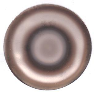
7 causing an increase in the diameter of the formed deposit. This is in agreement with that previously postulated by Nyaiesh 21. Plate (a) Plate (b) Plate (c) Plate (d) Plate (e) Plate (f) Fig. 4: Effects of gas type and target type on deposit diameter and colour due to sputtering the different targets at constant gas pressure of 0.05 mbar for 0.5 h: (a) Cu; (b) Ni; (c) Cu-10wt.%Ni (in dry Ar atmosphere). (d) Cu; (e) Ni; (f) Cu-10wt.%Ni (in dry 75%Ar+25%O 2 atmosphere). Plate (a) Plate (b) Plate (c) Plate (d) Plate (e) Plate (f) Fig. 5: Effects of gas type and target type on deposit diameter and colour due to sputtering the different targets at constant gas pressure of 0.1 mbar for 0.5 h: (a) Cu; (b) Ni; (c) Cu-10wt.%Ni (in dry Ar atmosphere). (d) Cu; (e) Ni; (f) Cu-10wt.%Ni (in dry 75%Ar+25%O 2 atmosphere). DOI: / Page
8 Figure No. Table 1: Deposit diameter (D) for the targets used (sputtering time = 0.5 h) Target Gas Type Gas Pressure (mbar) Deposit Diameter D (mm) Figure4. plate (a) Cu Ar Figure4. plate (b) Ni Ar Figure4. plate (c) Cu/Ni Ar Figure4. plate (d) Cu 75%Ar+25%O Figure4. plate (e) Ni 75%Ar+25%O Figure4. plate (f) Cu/Ni 75%Ar+25%O Figure5. plate (a) Cu Ar Figure5. plate (b) Ni Ar Figure5. plate (c) Cu/Ni Ar Figure5. plate (d) Cu 75%Ar+25%O Figure5. plate (e) Ni 75%Ar+25%O Figure5. plate (f) Cu/Ni 75%Ar+25%O VI. Conclusions: Different topics dealing with sputtering of Cu, Ni and Cu-10wt.%Ni targets in inert and active gas atmospheres using a dc planar magnetron sputtering system were conducted. The main conclusions were drawn as follows: I-V characteristics of Cu, Ni and Cu-Ni targets in dry atmospheres of Ar and Ar/O 2 showed that the Cu target gave greater current values at all values of applied voltages as compared with those of both Ni and Cu-Ni targets. I-V characteristics of the three targets in a gas mixture of Ar/O 2 at the same conditions of pressure and time showed hysteresis loops associated with higher current values than those obtained in dry Ar atmosphere. The area of the hysteresis loop (of each target) is related to the time period of the loop, it is larger at the lower time period and vice versa. Surface morphological features of sputtered Cu, Ni and Cu-Ni samples in dry Ar/O 2 atmosphere appeared to be more eroded than those observed in dry Ar atmosphere. The deposit diameter of the Cu/Ni target was larger than those obtained of both Cu and Ni targets, when sputtered separately under the same conditions. Adding oxygen gas (25%) to Ar glow discharge resulted in higher deposit diameters of the three targets than those obtained in Ar glow discharge. As the gas pressure was increased, the deposit diameter of each target was also increased. References [1]. Ohring, M., Materials science of thin films, 2nd edition, academic press, San Diego, New York, Boston, London. [2]. Kucharska, B. and E. Kulej, X-ray measurement of the Cu/Ni multilayer period. Archives of metallurgy and materials, 55, 1: [3]. Zhu, H.L., J. Y. Zhang, C. Z. Li, F. Pan, T. M. Wang, and B. B. Huang, Cu 2O thin films deposited by reactive direct current magnetron sputtering. Thin solid films, 517(19): [4]. Tvarozek, V., K. Shtereva, I. Novotny, J. Kovac, P. Sutta, R. Srnanek and A. Vincze, RF diode reactive sputtering of n-and p- type zinc oxide thin films. Vacuum, 82: [5]. Reddy, A.S., S. Uthanna and P.S. Reddy, Properties of dc magnetron sputtered Cu 2O films prepared at different sputtering pressures. Appl. Surf. Sci., 253(12): [6]. Jo, Y.D., K.N. Hui, K.S. Hui, Y.R. Cho and K.H. Kim, Microstructural, optical, and electrical properties of Ni Al co-doped ZnO films prepared by dc magnetron sputtering. Materials research bulletin, 51: [7]. Cen, J. and D. Wang, The metallization of PTC ceramic by magnetron sputtering. Physics procedia, 32: [8]. Mech, K., R. Kowalik and P. Zabinski, Cu thin films deposited by dc magnetron sputtering for contact surfaces on electronic components. Archives of metallurgy and materials, 56, 4: [9]. Kim, Nam-Hoon, Dong-Myong Na, Pil-Ju Ko, Jin-Seong Park and Woo-Sun Lee, Electrical and thermal properties of platinum thin films prepared by dc magnetron sputtering for micro-heater of microsensor applications after CMP process. Solid state phenomena vols., : [10]. Mugwang, F.K., P.K. Karimi, W.K. Njoroge, O. Omayio and S.M. Waita, Optical characterization of copper oxide thin films prepared by reactive dc magnetron sputtering for solar cell applications. Int. J. Thin Film Sci. Tec., 2 No. 1: [11]. Chernysh, V.S. and A.S. Patrakeev, Angular distribution of atoms sputtered from alloys. Nuclear instruments and methods in physics research B, 270: [12]. Wu, Chia-Che and Fan-Bean Wu, Microstructure and mechanical properties of magnetron co-sputtered Ni Al coatings. Surface & coatings technology, 204: DOI: / Page
9 [13]. Shulga, V.I., An attempt to solve andersen s puzzle in surface segregation during alloy sputtering. Nuclear instruments and methods in physics research B, 266: [14]. Soliman, H.N., H.M. Hosni and A. Rizk, Effects of physical sputtering and annealing temperature on surface behaviour of Cu-10wt.%Ni alloy, Accepted for publication in Egypt. J. Solids. [15]. Soliman, H.N. and A. Rizk, Effects of annealing temperatures on surface microtexturing and composition of Cu-10wt.%Ni- 2wt.%Sn alloy due to Ar + bombardment in a magnetron sputtering system. Current science international, 4: [16]. Carter, G. and J.S. Colligon, Ion bombardment of solids, New York, American Elsevier Pub. Co. [17]. Lam, N.Q. and K. Johannessen, Physical sputtering of Cu-Ni alloys: a molecular dynamics study. Nuclear instruments and methods in physics research B, 71: [18]. Kudriavtsev, Y., A. Villegas, A. Godines and R. Asomoza, Calculation of the surface binding energy for ion sputtered particles. Applied surface science, 239: [19]. Maniv, S. and W.D. Westwood, Discharge characteristics for magnetron sputtering of Al in Ar and Ar/O 2 mixtures. J. Vac. Sci.Technol., 17(3): 743. [20]. Rizk, N.S., A. Rizk and S.K. Habib, Redeposition of backscattered material in a dc magnetron sputtering system. Vacuum., 40(3): [21]. Nyaiesh, A.R., Target profile change during magnetron sputtering. Vacuum, 36(6): [22]. Nyaiesh, A.R. and L. Holland, Reactive magnetron sputtering of titanium and its oxides, J. Vac. Sci., Technol., 20: DOI: / Page
DEPOSITION OF THIN TiO 2 FILMS BY DC MAGNETRON SPUTTERING METHOD
 Chapter 4 DEPOSITION OF THIN TiO 2 FILMS BY DC MAGNETRON SPUTTERING METHOD 4.1 INTRODUCTION Sputter deposition process is another old technique being used in modern semiconductor industries. Sputtering
Gaetano L Episcopo. Scanning Electron Microscopy Focus Ion Beam and. Pulsed Plasma Deposition
 Gaetano L Episcopo Scanning Electron Microscopy Focus Ion Beam and Pulsed Plasma Deposition Hystorical background Scientific discoveries 1897: J. Thomson discovers the electron. 1924: L. de Broglie propose
A novel sputtering technique: Inductively Coupled Impulse Sputtering (ICIS)
") IOP Conference Series: Materials Science and Engineering A novel sputtering technique: Inductively Coupled Impulse Sputtering (ICIS) To cite this article: D A L Loch and A P Ehiasarian 2012 IOP Conf. Ser.:
IOP Conference Series: Materials Science and Engineering A novel sputtering technique: Inductively Coupled Impulse Sputtering (ICIS) To cite this article: D A L Loch and A P Ehiasarian 2012 IOP Conf. Ser.:
MICROCHIP MANUFACTURING by S. Wolf
 by S. Wolf Chapter 15 ALUMINUM THIN-FILMS and SPUTTER-DEPOSITION 2004 by LATTICE PRESS CHAPTER 15 - CONTENTS Aluminum Thin-Films Sputter-Deposition Process Steps Physics of Sputter-Deposition Magnetron-Sputtering
Metal Deposition. Filament Evaporation E-beam Evaporation Sputter Deposition
 Metal Deposition Filament Evaporation E-beam Evaporation Sputter Deposition 1 Filament evaporation metals are raised to their melting point by resistive heating under vacuum metal pellets are placed on
Plasma Deposition (Overview) Lecture 1
 Lecture 1") Plasma Deposition (Overview) Lecture 1 Material Processes Plasma Processing Plasma-assisted Deposition Implantation Surface Modification Development of Plasma-based processing Microelectronics needs (fabrication
Plasma Deposition (Overview) Lecture 1 Material Processes Plasma Processing Plasma-assisted Deposition Implantation Surface Modification Development of Plasma-based processing Microelectronics needs (fabrication
Combinatorial RF Magnetron Sputtering for Rapid Materials Discovery: Methodology and Applications
 Combinatorial RF Magnetron Sputtering for Rapid Materials Discovery: Methodology and Applications Philip D. Rack,, Jason D. Fowlkes,, and Yuepeng Deng Department of Materials Science and Engineering University
This is an author produced version of a paper presented at 2nd PATCMC, June 6th-8th 2011 Plzeň, Czech Republic.
 http://uu.diva-portal.org This is an author produced version of a paper presented at 2nd PATCMC, June 6th-8th 2011 Plzeň, Czech Republic. Kubart, T. 2011. Process modelling for reactive magnetron sputtering
TMT4320 Nanomaterials November 10 th, Thin films by physical/chemical methods (From chapter 24 and 25)
") 1 TMT4320 Nanomaterials November 10 th, 2015 Thin films by physical/chemical methods (From chapter 24 and 25) 2 Thin films by physical/chemical methods Vapor-phase growth (compared to liquid-phase growth)
1 TMT4320 Nanomaterials November 10 th, 2015 Thin films by physical/chemical methods (From chapter 24 and 25) 2 Thin films by physical/chemical methods Vapor-phase growth (compared to liquid-phase growth)
6.5 Optical-Coating-Deposition Technologies
 92 Chapter 6 6.5 Optical-Coating-Deposition Technologies The coating process takes place in an evaporation chamber with a fully controlled system for the specified requirements. Typical systems are depicted
Table of Content. Mechanical Removing Techniques. Ultrasonic Machining (USM) Sputtering and Focused Ion Beam Milling (FIB)
 Sputtering and Focused Ion Beam Milling (FIB)") Table of Content Mechanical Removing Techniques Ultrasonic Machining (USM) Sputtering and Focused Ion Beam Milling (FIB) Ultrasonic Machining In ultrasonic machining (USM), also called ultrasonic grinding,
Table of Content Mechanical Removing Techniques Ultrasonic Machining (USM) Sputtering and Focused Ion Beam Milling (FIB) Ultrasonic Machining In ultrasonic machining (USM), also called ultrasonic grinding,
Effects of plasma treatment on the precipitation of fluorine-doped silicon oxide
 ARTICLE IN PRESS Journal of Physics and Chemistry of Solids 69 (2008) 555 560 www.elsevier.com/locate/jpcs Effects of plasma treatment on the precipitation of fluorine-doped silicon oxide Jun Wu a,, Ying-Lang
Effect of Spiral Microwave Antenna Configuration on the Production of Nano-crystalline Film by Chemical Sputtering in ECR Plasma
 THE HARRIS SCIENCE REVIEW OF DOSHISHA UNIVERSITY, VOL. 56, No. 1 April 2015 Effect of Spiral Microwave Antenna Configuration on the Production of Nano-crystalline Film by Chemical Sputtering in ECR Plasma
Hysteresis-free reactive high power impulse magnetron sputtering
 Linköping University Postprint Hysteresis-free reactive high power impulse magnetron sputtering E. Wallin and U. Helmersson N.B.: When citing this work, cite the original article. Original publication:
Inductively Coupled Plasma Reactive Ion Etching of GeSbTe Thin Films in a HBr/Ar Gas
 Integrated Ferroelectrics, 90: 95 106, 2007 Copyright Taylor & Francis Group, LLC ISSN 1058-4587 print / 1607-8489 online DOI: 10.1080/10584580701249371 Inductively Coupled Plasma Reactive Ion Etching
 http://www.diva-portal.org This is the published version of a paper presented at Invited talk: 12th International Symposium on Sputtering and Plasma Processes, Kyoto, July 10-12, 2013. Citation for the
Sputter Ion Pump (Ion Pump) By Biswajit
 By Biswajit") Sputter Ion Pump (Ion Pump) By Biswajit 08-07-17 Sputter Ion Pump (Ion Pump) An ion pump is a type of vacuum pump capable of reaching pressures as low as 10 11 mbar under ideal conditions. An ion pump
Sputter Ion Pump (Ion Pump) By Biswajit 08-07-17 Sputter Ion Pump (Ion Pump) An ion pump is a type of vacuum pump capable of reaching pressures as low as 10 11 mbar under ideal conditions. An ion pump
PHYSICAL VAPOR DEPOSITION OF THIN FILMS
 PHYSICAL VAPOR DEPOSITION OF THIN FILMS JOHN E. MAHAN Colorado State University A Wiley-Interscience Publication JOHN WILEY & SONS, INC. New York Chichester Weinheim Brisbane Singapore Toronto CONTENTS
Lecture 6 Plasmas. Chapters 10 &16 Wolf and Tauber. ECE611 / CHE611 Electronic Materials Processing Fall John Labram 1/68
 Lecture 6 Plasmas Chapters 10 &16 Wolf and Tauber 1/68 Announcements Homework: Homework will be returned to you on Thursday (12 th October). Solutions will be also posted online on Thursday (12 th October)
Technology for Micro- and Nanostructures Micro- and Nanotechnology
 Lecture 10: Deposition Technology for Micro- and Nanostructures Micro- and Nanotechnology Peter Unger mailto: peter.unger @ uni-ulm.de Institute of Optoelectronics University of Ulm http://www.uni-ulm.de/opto
Modification of Thin Film Properties by Sputtered Particles
 1 Modification of Thin Film Properties by Sputtered Particles Yasunori Taga 1. Introduction The novelty of the functions provided by plasma-assisted physical vapor deposition films, together with their
Reactive magnetron sputter deposition: a journey from target to substrate
 Reactive magnetron sputter deposition: a journey from target to substrate D. Depla Dedicated Research on Advanced Films and Targets Ghent University Setting the scene Who? Some keywords Main features of
Some more equations describing reactive magnetron sputtering.
 Some more equations describing reactive magnetron sputtering D. Depla, S. Mahieu, W. Leroy, K. Van Aeken, J. Haemers, R. De Gryse www.draft.ugent.be discharge voltage (V) 44 4 36 32 28..5 1. 1.5 S (Pumping
Energy fluxes in plasmas for fabrication of nanostructured materials
 Energy fluxes in plasmas for fabrication of nanostructured materials IEAP, Universität Kiel 2nd Graduate Summer Institute "Complex Plasmas" August 5-13, 2010 in Greifswald (Germany) AG 1 Outline Motivation
Plasma processes under low and atmospheric pressure.
 Plasma processes under low and atmospheric pressure. O.Kylián, J. Hanuš, A. Choukourov, J. Kousal, A. Kuzminova, P. Solar, A. Shelemin, H. Biederman Charles University in Prague Faculty of Mathematics
1 EX/P4-8. Hydrogen Concentration of Co-deposited Carbon Films Produced in the Vicinity of Local Island Divertor in Large Helical Device
 1 EX/P4-8 Hydrogen Concentration of Co-deposited Carbon Films Produced in the Vicinity of Local Island Divertor in Large Helical Device T. Hino 1,2), T. Hirata 1), N. Ashikawa 2), S. Masuzaki 2), Y. Yamauchi
Inductively Coupled Plasma Etching of Ta, Co, Fe, NiFe, NiFeCo, and MnNi with Cl 2 /Ar Discharges
 Korean J. Chem. Eng., 21(6), 1235-1239 (2004) Inductively Coupled Plasma Etching of Ta, Co, Fe, NiFe, NiFeCo, and MnNi with Cl 2 /Ar Discharges Hyung Jo Park*, Hyun-Wook Ra, Kwang Sup Song** and Yoon-Bong
Repetition: Practical Aspects
 Repetition: Practical Aspects Reduction of the Cathode Dark Space! E x 0 Geometric limit of the extension of a sputter plant. Lowest distance between target and substrate V Cathode (Target/Source) - +
Highly stable and flexible Li-ion battery anodes based on TiO 2 coated
 Electronic Supplementary Material (ESI) for Journal of Materials Chemistry A. This journal is The Royal Society of Chemistry 2015 Supporting Information for Highly stable and flexible Li-ion battery anodes
ION BOMBARDMENT CHARACTERISTICS DURING THE GROWTH OF OPTICAL FILMS USING A COLD CATHODE ION SOURCE
 ION BOMBARDMENT CHARACTERISTICS DURING THE GROWTH OF OPTICAL FILMS USING A COLD CATHODE ION SOURCE O. Zabeida, J.E. Klemberg-Sapieha, and L. Martinu, Ecole Polytechnique, Department of Engineering Physics
PIC/MCC Simulation of Radio Frequency Hollow Cathode Discharge in Nitrogen
 PIC/MCC Simulation of Radio Frequency Hollow Cathode Discharge in Nitrogen HAN Qing ( ), WANG Jing ( ), ZHANG Lianzhu ( ) College of Physics Science and Information Engineering, Hebei Normal University,
Reduced preferential sputtering of TiO 2 (and Ta 2 O 5 ) thin films through argon cluster ion bombardment.
 thin films through argon cluster ion bombardment.") NATIOMEM Reduced preferential sputtering of TiO 2 (and Ta 2 O 5 ) thin films through argon cluster ion bombardment. R. Grilli *, P. Mack, M.A. Baker * * University of Surrey, UK ThermoFisher Scientific
NATIOMEM Reduced preferential sputtering of TiO 2 (and Ta 2 O 5 ) thin films through argon cluster ion bombardment. R. Grilli *, P. Mack, M.A. Baker * * University of Surrey, UK ThermoFisher Scientific
LECTURE 5 SUMMARY OF KEY IDEAS
 LECTURE 5 SUMMARY OF KEY IDEAS Etching is a processing step following lithography: it transfers a circuit image from the photoresist to materials form which devices are made or to hard masking or sacrificial
Surface Characteristics of a Polyimide Film Treated with a Dielectric Barrier Discharge Plasma
 Journal of the Korean Physical Society, Vol. 54, No. 3, March 2009, pp. 11561160 Surface Characteristics of a Polyimide Film Treated with a Dielectric Barrier Discharge Plasma S. M. Kang, W. J. Park and
Section 5: Thin Film Deposition part 1 : sputtering and evaporation. Jaeger Chapter 6. EE143 Ali Javey
 Section 5: Thin Film Deposition part 1 : sputtering and evaporation Jaeger Chapter 6 Vacuum Basics 1. Units 1 atmosphere = 760 torr = 1.013x10 5 Pa 1 bar = 10 5 Pa = 750 torr 1 torr = 1 mm Hg 1 mtorr =
Secondary ion mass spectrometry (SIMS)
") Secondary ion mass spectrometry (SIMS) ELEC-L3211 Postgraduate Course in Micro and Nanosciences Department of Micro and Nanosciences Personal motivation and experience on SIMS Offers the possibility to
Secondary ion mass spectrometry (SIMS) ELEC-L3211 Postgraduate Course in Micro and Nanosciences Department of Micro and Nanosciences Personal motivation and experience on SIMS Offers the possibility to
Auger Electron Spectroscopy (AES) Prof. Paul K. Chu
 Prof. Paul K. Chu") Auger Electron Spectroscopy (AES) Prof. Paul K. Chu Auger Electron Spectroscopy Introduction Principles Instrumentation Qualitative analysis Quantitative analysis Depth profiling Mapping Examples The Auger
Auger Electron Spectroscopy (AES) Prof. Paul K. Chu Auger Electron Spectroscopy Introduction Principles Instrumentation Qualitative analysis Quantitative analysis Depth profiling Mapping Examples The Auger
Auger Electron Spectroscopy
 Auger Electron Spectroscopy Auger Electron Spectroscopy is an analytical technique that provides compositional information on the top few monolayers of material. Detect all elements above He Detection
PHYSICAL AND CHEMICAL PROPERTIES OF ATMOSPHERIC PRESSURE PLASMA POLYMER FILMS
 PHYSICAL AND CHEMICAL PROPERTIES OF ATMOSPHERIC PRESSURE PLASMA POLYMER FILMS O. Goossens, D. Vangeneugden, S. Paulussen and E. Dekempeneer VITO Flemish Institute for Technological Research, Boeretang
Modelling of the Target Voltage Behaviour in Reactive Sputtering R. De Gryse*, D. Depla University Ghent, Krijgslaan 281/S1, B-9000 GENT, Belgium
 Modelling of the Target Voltage Behaviour in Reactive Sputtering R. De Gryse*, D. Depla University Ghent, Krijgslaan 28/S, B-9 GENT, Belgium Abstract It has been shown that at least two mechanisms are
Nova 600 NanoLab Dual beam Focused Ion Beam IITKanpur
 Nova 600 NanoLab Dual beam Focused Ion Beam system @ IITKanpur Dual Beam Nova 600 Nano Lab From FEI company (Dual Beam = SEM + FIB) SEM: The Electron Beam for SEM Field Emission Electron Gun Energy : 500
EE143 Fall 2016 Microfabrication Technologies. Lecture 6: Thin Film Deposition Reading: Jaeger Chapter 6
 EE143 Fall 2016 Microfabrication Technologies Lecture 6: Thin Film Deposition Reading: Jaeger Chapter 6 Prof. Ming C. Wu wu@eecs.berkeley.edu 511 Sutardja Dai Hall (SDH) 1 Vacuum Basics Units 1 atmosphere
Electron beam scanning
 Electron beam scanning The Electron beam scanning operates through an electro-optical system which has the task of deflecting the beam Synchronously with cathode ray tube which create the image, beam moves
Contents. Bibliografische Informationen digitalisiert durch
 1 Simulation of the Sputtering Process T. Ono, T. Kenmotsu, and T. Muramoto 1 1.1 Introduction 1 1.2 Computer Simulation Codes 2 1.3 Total Sputtering Yield 5 1.3.1 Incident-Energy Dependence of Sputtering
Solutions for Assignment-6
 Solutions for Assignment-6 Q1. What is the aim of thin film deposition? [1] (a) To maintain surface uniformity (b) To reduce the amount (or mass) of light absorbing materials (c) To decrease the weight
Applications of Micro-Area Analysis Used by JPS-9200 X-ray Photoelectron Spectrometer
 Applications of Micro-Area Analysis Used by JPS-9200 X-ray Photoelectron Spectrometer Yoshitoki Iijima Application & Research Center, JEOL Ltd. Introduction Recently, with advances in the development of
Improvement of MgO Characteristics Using RF-Plasma Treatment in AC Plasma Display Panel
 Mol. Cryst. Liq. Cryst., Vol. 531: pp. 73=[373] 81=[381], 2010 Copyright # Taylor & Francis Group, LLC ISSN: 1542-1406 print=1563-5287 online DOI: 10.1080/15421406.2010.499331 Improvement of MgO Characteristics
The Computational Simulation of the Positive Ion Propagation to Uneven Substrates
 WDS' Proceedings of Contributed Papers, Part II, 5 9,. ISBN 978-8-778-85-9 MATFYZPRESS The Computational Simulation of the Positive Ion Propagation to Uneven Substrates V. Hrubý and R. Hrach Charles University,
Bi-directional phase transition of Cu/6H SiC( ) system discovered by positron beam study
 system discovered by positron beam study") Applied Surface Science 194 (2002) 278 282 Bi-directional phase transition of Cu/6H SiC(0 0 0 1) system discovered by positron beam study J.D. Zhang a,*, H.M. Weng b, Y.Y. Shan a, H.M. Ching a, C.D. Beling
Applied Surface Science 194 (2002) 278 282 Bi-directional phase transition of Cu/6H SiC(0 0 0 1) system discovered by positron beam study J.D. Zhang a,*, H.M. Weng b, Y.Y. Shan a, H.M. Ching a, C.D. Beling
Supplementary Figure 1 Detailed illustration on the fabrication process of templatestripped
 Supplementary Figure 1 Detailed illustration on the fabrication process of templatestripped gold substrate. (a) Spin coating of hydrogen silsesquioxane (HSQ) resist onto the silicon substrate with a thickness
Electrochemical Deposition of Iron Nanoparticles on PPY and H terminated Si substrates. Karan Sukhija Co-op Term # 1 April 28 th, 2005
 Electrochemical Deposition of Iron Nanoparticles on PPY and H terminated Si substrates Karan Sukhija Co-op Term # 1 April 28 th, 2005 Future Suggested Experiments Acknowledgments Presentation Outline Background
Quasi-periodic nanostructures grown by oblique angle deposition
 JOURNAL OF APPLIED PHYSICS VOLUME 94, NUMBER 12 15 DECEMBER 2003 Quasi-periodic nanostructures grown by oblique angle deposition T. Karabacak, a) G.-C. Wang, and T.-M. Lu Department of Physics, Applied
Appearance Potential Spectroscopy
 Appearance Potential Spectroscopy Submitted by Sajanlal P. R CY06D009 Sreeprasad T. S CY06D008 Dept. of Chemistry IIT MADRAS February 2006 1 Contents Page number 1. Introduction 3 2. Theory of APS 3 3.
TOPOGRAPHY STUDIES OF A MAGNETRON REACTIVE SPUTTERED COATING
 U.P.B. Sci. Bull., Series B, Vol. 75, Iss. 3, 2013 ISSN 1454-2331 TOPOGRAPHY STUDIES OF A MAGNETRON REACTIVE SPUTTERED COATING Ileana ŞTEFĂNESCU 1, Ion CIUCĂ 2 The present paper shows changes of the morphological
Fig 1: Auger Electron Generation (a) Step 1 and (b) Step 2
 Step 1 and (b) Step 2") Auger Electron Spectroscopy (AES) Physics of AES: Auger Electrons were discovered in 1925 but were used in surface analysis technique in 1968. Auger Electron Spectroscopy (AES) is a very effective method
Auger Electron Spectroscopy (AES) Physics of AES: Auger Electrons were discovered in 1925 but were used in surface analysis technique in 1968. Auger Electron Spectroscopy (AES) is a very effective method
Simulation of the cathode surface damages in a HOPFED during ion bombardment
 Simulation of the cathode surface damages in a HOPFED during ion bombardment Hongping Zhao, Wei Lei, a Xiaobing Zhang, Xiaohua Li, and Qilong Wang Department of Electronic Engineering, Southeast University,
THE PROPERTIES OF THIN FILM DIELECTRIC LAYERS PREPARED BY SPUTTERING
 THE PROPERTIES OF THIN FILM DIELECTRIC LAYERS PREPARED BY SPUTTERING Ivana BESHAJOVÁ PELIKÁNOVÁ a, Libor VALENTA a a KATEDRA ELEKTROTECHNOLOGIE, ČVUT FEL, Technická 2, 166 27 Praha 6, Česká republika,
Etching Issues - Anisotropy. Dry Etching. Dry Etching Overview. Etching Issues - Selectivity
 Etching Issues - Anisotropy Dry Etching Dr. Bruce K. Gale Fundamentals of Micromachining BIOEN 6421 EL EN 5221 and 6221 ME EN 5960 and 6960 Isotropic etchants etch at the same rate in every direction mask
Soft X-ray multilayer mirrors by ion assisted sputter deposition
 Soft X-ray multilayer mirrors by ion assisted sputter deposition Valentino Rigato INFN Laboratori Nazionali di Legnaro Bologna, September 21, 2010 Source: INFN-LNL-2009 V. RIGATO 1 SIF- Bologna September
Control of Optical Properties by the Stepwise Chemical and Plasma Spray Treatment of Polycarbonate
 Appl. Sci. Converg. Technol. 27(6): 135-139 (2018) https://doi.org/10.5757/asct.2018.27.6.135 Research Paper Control of Optical Properties by the Stepwise Chemical and Plasma Spray Treatment of Polycarbonate
UNIT 3. By: Ajay Kumar Gautam Asst. Prof. Dev Bhoomi Institute of Technology & Engineering, Dehradun
 UNIT 3 By: Ajay Kumar Gautam Asst. Prof. Dev Bhoomi Institute of Technology & Engineering, Dehradun 1 Syllabus Lithography: photolithography and pattern transfer, Optical and non optical lithography, electron,
The role of recycling in pulsed sputtering magnetrons
 The role of recycling in pulsed sputtering magnetrons Jón Tómas Guðmundsson 1,2,3, Daniel Lundin 3, Michael A. Raadu 1, Thomas J. Petty 3, Tiberiu M. Minea 3, and Nils Brenning 1 1 Department of Space
Repetition: Ion Plating
 Repetition: Ion Plating Substrate HV (bis ca. 1kV) Optional ionization system Source Ionized filling gas Source material, ionized or neutral Repetition: Ion Plating Ion Species Separated ion source Ions
PRINCIPLES OF PLASMA DISCHARGES AND MATERIALS PROCESSING
 PRINCIPLES OF PLASMA DISCHARGES AND MATERIALS PROCESSING Second Edition MICHAEL A. LIEBERMAN ALLAN J, LICHTENBERG WILEY- INTERSCIENCE A JOHN WILEY & SONS, INC PUBLICATION CONTENTS PREFACE xrrii PREFACE
Introduction to Thin Film Processing
 Introduction to Thin Film Processing Deposition Methods Many diverse techniques available Typically based on three different methods for providing a flux of atomic or molecular material Evaporation Sputtering
Electrical Discharges Characterization of Planar Sputtering System
 International Journal of Recent Research and Review, Vol. V, March 213 ISSN 2277 8322 Electrical Discharges Characterization of Planar Sputtering System Bahaa T. Chaid 1, Nathera Abass Ali Al-Tememee 2,
Song Fengqi, Zhang Lu, Zhu Lianzhong, Ge Jun, Wang Guanghou *
 Low energy cluster beam deposited BN films as the cascade for Field Emission 一 Song Fengqi, Zhang Lu, Zhu Lianzhong, Ge Jun, Wang Guanghou * National laboratory of Solid State Microstructures, Department
Effect of Sample Configuration on Droplet-Particles of TiN Films Deposited by Pulse Biased Arc Ion Plating
 J. Mater. Sci. Technol., Vol.25 No.5, 29 681 Effect of Sample Configuration on Droplet-Particles of TiN Films Deposited by Pulse Biased Arc Ion Plating Yanhui Zhao 1), Guoqiang Lin 2), Jinquan Xiao 1),
CHAPTER 6: Etching. Chapter 6 1
 Chapter 6 1 CHAPTER 6: Etching Different etching processes are selected depending upon the particular material to be removed. As shown in Figure 6.1, wet chemical processes result in isotropic etching
X-ray photoelectron spectroscopic characterization of molybdenum nitride thin films
 Korean J. Chem. Eng., 28(4), 1133-1138 (2011) DOI: 10.1007/s11814-011-0036-2 INVITED REVIEW PAPER X-ray photoelectron spectroscopic characterization of molybdenum nitride thin films Jeong-Gil Choi Department
Supporting Information for. Selectivity and Activity in Catalytic Methanol Oxidation in the Gas Phase
 1 / 5 Supporting Information for The Influence of Size-Induced Oxidation State of Platinum Nanoparticles on Selectivity and Activity in Catalytic Methanol Oxidation in the Gas Phase Hailiang Wang, Yihai
ION Pumps for UHV Systems, Synchrotrons & Particle Accelerators. Mauro Audi, Academic, Government & Research Marketing Manager
 ION Pumps for UHV Systems, Synchrotrons & Particle Accelerators Mauro Audi, Academic, Government & Research Marketing Manager ION Pumps Agilent Technologies 1957-59 Varian Associates invents the first
Off-axis unbalanced magnetron sputtering of YBa2Cu307 thin films
 ELSEVIER Materials Chemistry and Physics 49 (1997) 229-233 MATERIALS CHEMISTRYAND PHYSICS Off-axis unbalanced magnetron sputtering of YBa2Cu307 thin films Wen-Chou Tsai, Tseung-Yuen Tseng * Institute of
Competitive Advantages of Ontos7 Atmospheric Plasma
 Competitive Advantages of Ontos7 Atmospheric Plasma Eric Schulte Matt Phillips Keith Cooper SETNA Proprietary 1 Advantages of Ontos7 Atmospheric Plasma Process over Vacuum RIE Plasma for Die/Wafer Surface
Keywords. 1=magnetron sputtering, 2= rotatable cathodes, 3=substrate temperature, 4=anode. Abstract
 Managing Anode Effects and Substrate Heating from Rotatable Sputter Targets. F. Papa*, V. Bellido-Gonzalez**, Alex Azzopardi**, Dr. Dermot Monaghan**, *Gencoa Technical & Business Support in US, Davis,
Simulation of Metal TRAnport. SIMTRA : a tool to predict and understand deposition. K. Van Aeken, S. Mahieu, D. Depla.
 Simulation of Metal TRAnport SIMTRA : a tool to predict and understand deposition K. Van Aeken, S. Mahieu, D. Depla www.draft.ugent.be 1) : Why do we calculate? ) Scientific background : How do we calculate?
Thin Film Bi-based Perovskites for High Energy Density Capacitor Applications
 ..SKELETON.. Thin Film Bi-based Perovskites for High Energy Density Capacitor Applications Colin Shear Advisor: Dr. Brady Gibbons 2010 Table of Contents Chapter 1 Introduction... 1 1.1 Motivation and Objective...
Gold nanothorns macroporous silicon hybrid structure: a simple and ultrasensitive platform for SERS
 Supporting Information Gold nanothorns macroporous silicon hybrid structure: a simple and ultrasensitive platform for SERS Kamran Khajehpour,* a Tim Williams, b,c Laure Bourgeois b,d and Sam Adeloju a
Nanostructure. Materials Growth Characterization Fabrication. More see Waser, chapter 2
 Nanostructure Materials Growth Characterization Fabrication More see Waser, chapter 2 Materials growth - deposition deposition gas solid Physical Vapor Deposition Chemical Vapor Deposition Physical Vapor
Scaling during shadowing growth of isolated nanocolumns
 Scaling during shadowing growth of isolated nanocolumns T. Karabacak, J. P. Singh, Y.-P. Zhao, G.-C. Wang, and T.-M. Lu Department of Physics, Applied Physics and Astronomy, Rensselaer Polytechnic Institute,
Auger Electron Spectroscopy Overview
 Auger Electron Spectroscopy Overview Also known as: AES, Auger, SAM 1 Auger Electron Spectroscopy E KLL = E K - E L - E L AES Spectra of Cu EdN(E)/dE Auger Electron E N(E) x 5 E KLL Cu MNN Cu LMM E f E
- A spark is passed through the Argon in the presence of the RF field of the coil to initiate the plasma
 THE PLASMA Inductively Coupled Plasma Mass Spectrometry (ICP-MS) What is a Plasma? - The magnetic field created by a RF (radio frequency) coil produces a current within a stream of Argon (Ar) gas, which
Large Scale Direct Synthesis of Graphene on Sapphire and Transfer-free Device Fabrication
 Supplementary Information Large Scale Direct Synthesis of Graphene on Sapphire and Transfer-free Device Fabrication Hyun Jae Song a, Minhyeok Son a, Chibeom Park a, Hyunseob Lim a, Mark P. Levendorf b,
Depth Distribution Functions of Secondary Electron Production and Emission
 Depth Distribution Functions of Secondary Electron Production and Emission Z.J. Ding*, Y.G. Li, R.G. Zeng, S.F. Mao, P. Zhang and Z.M. Zhang Hefei National Laboratory for Physical Sciences at Microscale
Fabrication Technology, Part I
 EEL5225: Principles of MEMS Transducers (Fall 2004) Fabrication Technology, Part I Agenda: Microfabrication Overview Basic semiconductor devices Materials Key processes Oxidation Thin-film Deposition Reading:
Ionization Techniques Part IV
 Ionization Techniques Part IV CU- Boulder CHEM 5181 Mass Spectrometry & Chromatography Presented by Prof. Jose L. Jimenez High Vacuum MS Interpretation Lectures Sample Inlet Ion Source Mass Analyzer Detector
Chapter 3 Engineering Science for Microsystems Design and Fabrication
 Lectures on MEMS and MICROSYSTEMS DESIGN and MANUFACTURE Chapter 3 Engineering Science for Microsystems Design and Fabrication In this Chapter, we will present overviews of the principles of physical and
Defense Technical Information Center Compilation Part Notice
 UNCLASSIFIED Defense Technical Information Center Compilation Part Notice ADP012830 TITLE: XPS Study of Cu-Clusters and Atoms in Cu/SiO2 Composite Films DISTRIBUTION: Approved for public release, distribution
Auger Electron Spectroscopy (AES)
") 1. Introduction Auger Electron Spectroscopy (AES) Silvia Natividad, Gabriel Gonzalez and Arena Holguin Auger Electron Spectroscopy (Auger spectroscopy or AES) was developed in the late 1960's, deriving
1. Introduction Auger Electron Spectroscopy (AES) Silvia Natividad, Gabriel Gonzalez and Arena Holguin Auger Electron Spectroscopy (Auger spectroscopy or AES) was developed in the late 1960's, deriving
Supporting Information. Temperature dependence on charge transport behavior of threedimensional
 Supporting Information Temperature dependence on charge transport behavior of threedimensional superlattice crystals A. Sreekumaran Nair and K. Kimura* University of Hyogo, Graduate School of Material
Atomic layer deposition of titanium nitride
 Atomic layer deposition of titanium nitride Jue Yue,version4, 04/26/2015 Introduction Titanium nitride is a hard and metallic material which has found many applications, e.g.as a wear resistant coating[1],
ELEMENT2 High Resolution- ICP-MS INSTRUMENT OVERVIEW
 ELEMENT2 High Resolution- ICP-MS INSTRUMENT OVERVIEW Inductively Coupled Plasma Mass Spectrometry (ICP-MS) What is a Plasma? - The magnetic field created by a RF (radio frequency) coil produces
Ion sputtering yield coefficients from In thin films bombarded by different energy Ar + ions
 Ion sputtering yield coefficients from thin films bombarded by different energy Ar + ions MJ Madito, H Swart and JJ Terblans 1 Department of Physics, University of the Free State, P.. Box 339, Bloemfontein,
High-Current Y-Ba-Cu-O Coated Conductor using Metal Organic Chemical-Vapor Deposition and Ion-Beam-Assisted Deposition
 SP-T-152 High-Current Y-Ba-Cu-O Coated Conductor using Metal Organic Chemical-Vapor Deposition and Ion-Beam-Assisted Deposition V. Selvamanickam, G. Carota, M. Funk, N. Vo, and P. Haldar U. Balachandran,
ARGON RF PLASMA TREATMENT OF PET FILMS FOR SILICON FILMS ADHESION IMPROVEMENT
 Journal of Optoelectronics and Advanced Materials Vol. 7, No. 5, October 2005, p. 2529-2534 ARGON RF PLASMA TREATMENT OF FILMS FOR SILICON FILMS ADHESION IMPROVEMENT I. A. Rusu *, G. Popa, S. O. Saied
PHI 5000 Versaprobe-II Focus X-ray Photo-electron Spectroscopy
 PHI 5000 Versaprobe-II Focus X-ray Photo-electron Spectroscopy The very basic theory of XPS XPS theroy Surface Analysis Ultra High Vacuum (UHV) XPS Theory XPS = X-ray Photo-electron Spectroscopy X-ray
Electrodeposited nickel hydroxide on nickel foam with ultrahigh. capacitance
 Electrodeposited nickel hydroxide on nickel foam with ultrahigh capacitance Guang-Wu Yang, Cai-Ling Xu* and Hu-Lin Li* College of Chemistry and Chemical Engineering, Lanzhou University, 73 (PR China) 1.
QUESTIONS AND ANSWERS
 QUESTIONS AND ANSWERS (1) For a ground - state neutral atom with 13 protons, describe (a) Which element this is (b) The quantum numbers, n, and l of the inner two core electrons (c) The stationary state
Effect of Electrolyte Concentration during Solution Plasma on Copper Nanoparticle Size
 IOP Conference Series: Materials Science and Engineering PAPER OPEN ACCESS Effect of Electrolyte Concentration during Solution Plasma on Copper Nanoparticle Size To cite this article: M H S Al Anbouri
Electrostatic Bonding of Silicon-to-ITO coated #7059 Glass using Li-doped Oxide Interlayer
 Journal of the Korean Physical Society, Vol. 33, No., November 1998, pp. S406 S410 Electrostatic Bonding of Silicon-to-ITO coated #7059 Glass using Li-doped Oxide Interlayer Jee-Won Jeong, Byeong-Kwon