My Research. Adam Rosowski. Photonic in Engineering GROUP
|
|
|
- Angela Johnston
- 5 years ago
- Views:
Transcription
1 My Research Adam Rosowski Photonic in Engineering
2 Photo onic in Engineering Motivation Chemical etching process Direct laser process HCL Technology Therahertz spectroskopy Physics

3 Motivation Photonic in Engineering
4 Motivation Photo onic in Engineering MEMS elements: Size: 1-200µm Materials: semicondutors (Si, SiC, GaAS, etc.), ceramics, glass, polymers Structures: membrans, cantilevers, channels, blades and another microdetails
5 State of art Photo onic in Engineering Present technologies: Wet chemical etching in solution (eg. KOH, NaOH, HNO 3 + HF) Dry physical etching (eg. RIE, laser)
6 Photo onic in Engineering Motivation Chemical etching process Direct laser process HCL Technology Therahertz spectroskopy Physics
7 Chemical etching in base Photo onic in Engineering Basic process: Si + 2(OH) - + 4H 2 O Si(OH) H 2 Speed of etching: V E = a V0 exp kt
8 Chemical etching in base Etch rate (µm/min) Photo onic in Engineering Echant Temperature Si (100) Si (110) Si (111) % KOH % KOH % KOH
9 Chemical etching Photo onic in Engineering Advantages: High quality of etched structures Batch-process low cost of one unit Disadvantages: Low speed of etching Lithography processes Difficulties with complex structures and different materials
10 Photo onic in Engineering Motivation Chemical etching process Direct laser process HCL Technology Therahertz spectroskopy Physics
11 Direct laser process Photo onic in Engineering Advantages: High speed of etching Direct process without lithography Simple for diffrent materials Disadvantages: Poor quality Difficulties with batch-process


12 Experimental setup Photo onic in Engineering SPI G3: 1070nm, ns, kHz Coherent Avia: 355nm, 30ns, kHz Spectra-Physics Pantera: 355nm, 50ps, 80MHz


13 Direct laser process Photonic in Engineering
14 Photo onic in Engineering Motivation Chemical etching process Direct laser process HCL Technology Therahertz spectroskopy Physics
15 HCL technology Photo onic in Engineering Connection between chemical and laser etching: Laser direct processing and post-processing in solution; Laser ablation in solution; Chemical process activated and assited with laser beam: Laser beam increases local temperature of liquid and surface (higher etching rate) Laser beam decreases chemical activation energy locally Solution etches locally (high quality) Laser beam increases reactivity of OH - ions
16 HCL technology Photo onic in Engineering Advanatages: High quality High etching speed Direct process without lithography Simple for different materials (wide band gap semiconductors) and difficult structures Disadvanatages: Problems with batch-process
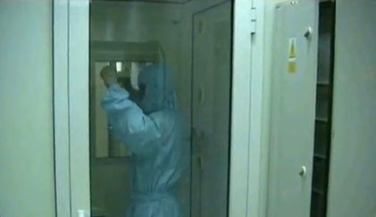
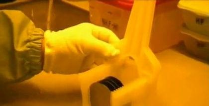
17 Experimental setup Photo onic in Engineering Processing chamber Pumping system Temperature control Scan head Laser: SPI G3 Specra Physics Pantera / Coherent Avia Diode laser Solution: KOH/NaOH
18 Results Chemical etching HCL technology Photonic in Engineering
19 Results Photo onic in Engineering Direct laser process HCL technology

20 Results - mistakes Photonic in Engineering
21 Photo onic in Engineering Motivation Chemical etching process Direct laser process HCL Technology Therahertz spectroskopy Physics


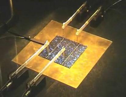
22 Terahertz radiation Photonic in Engineering
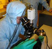
23 Art spectroscopy Photonic in Engineering Dr Michael Panzner
24 Time-domain spectroscopy Photonic in Engineering
25 Software Photonic in Engineering With Dr Michael Panzner
26 Results Photonic in Engineering With Dr Michael Panzner
27 Photo onic in Engineering Places of my research: Fraunhofer IWS, Dresden, Germany: 2008, 2009, 2011, 2012 Lappenranta Laser Processing Centre (VTT and University of Technology), Lappeenranta, Finland, 2009, 2010 Photonics in Engineering Group, Liverpool John Moores University, Liverpool, UK, 2010
28 Photo onic in Engineering Motivation Chemical etching process Direct laser process HCL Technology Therahertz spectroskopy Physics
29 onic in Engineering Relativistic transformation Lorenz transformation: where: Conclusions: ( ) = = 2 ' ' c vx t t vt x x γ c v = = β β γ, ; v l l t t = = Photo How???? ; 1 c l l c v t = = β β = = = T T T T T T
30 Maxwell vs Jüttner Distribution Photo onic in Engineering We cannot measure (the black holes, the centre of stars, etc.)
31 Confirmation Photo onic in Engineering Computer simulation only 1D and 2D gases were done; 3D Monte Carlo only Problems: Huge number of balls Relativistic transformation (!) Definition of temperature Program: Method: deterministic model Environment: MatLab It has to work with huge numbers of balls Extreme optimisation of memory use and processor utilisation
32 Results Photonic in Engineering
33 Photo onic in Engineering Thank you for your attention Adam Rosowski
UNIT 3. By: Ajay Kumar Gautam Asst. Prof. Dev Bhoomi Institute of Technology & Engineering, Dehradun
 UNIT 3 By: Ajay Kumar Gautam Asst. Prof. Dev Bhoomi Institute of Technology & Engineering, Dehradun 1 Syllabus Lithography: photolithography and pattern transfer, Optical and non optical lithography, electron,
Free-Space MEMS Tunable Optical Filter in (110) Silicon
 Silicon") Free-Space MEMS Tunable Optical Filter in (110) Silicon Ariel Lipson & Eric M. Yeatman Optical & Semiconductor Group Outline Device - Optical Filter Optical analysis Fabrication Schematic Fabricated 2
Free-Space MEMS Tunable Optical Filter in (110) Silicon Ariel Lipson & Eric M. Yeatman Optical & Semiconductor Group Outline Device - Optical Filter Optical analysis Fabrication Schematic Fabricated 2
Etching: Basic Terminology
 Lecture 7 Etching Etching: Basic Terminology Introduction : Etching of thin films and sometimes the silicon substrate are very common process steps. Usually selectivity, and directionality are the first
EE 527 MICROFABRICATION. Lecture 24 Tai-Chang Chen University of Washington
 EE 527 MICROFABRICATION Lecture 24 Tai-Chang Chen University of Washington EDP ETCHING OF SILICON - 1 Ethylene Diamine Pyrocatechol Anisotropy: (100):(111) ~ 35:1 EDP is very corrosive, very carcinogenic,
Self-Assembled InAs Quantum Dots
 Self-Assembled InAs Quantum Dots Steve Lyon Department of Electrical Engineering What are semiconductors What are semiconductor quantum dots How do we make (grow) InAs dots What are some of the properties
CHAPTER 6: Etching. Chapter 6 1
 Chapter 6 1 CHAPTER 6: Etching Different etching processes are selected depending upon the particular material to be removed. As shown in Figure 6.1, wet chemical processes result in isotropic etching
Development and characterization of 3D semiconductor X-rays detectors for medical imaging
 Development and characterization of 3D semiconductor X-rays detectors for medical imaging Marie-Laure Avenel, Eric Gros d Aillon CEA-LETI, DETectors Laboratory marie-laure.avenel@cea.fr Outlines Problematic
Wet and Dry Etching. Theory
 Wet and Dry Etching Theory 1. Introduction Etching techniques are commonly used in the fabrication processes of semiconductor devices to remove selected layers for the purposes of pattern transfer, wafer
Lithography and Etching
 Lithography and Etching Victor Ovchinnikov Chapters 8.1, 8.4, 9, 11 Previous lecture Microdevices Main processes: Thin film deposition Patterning (lithography) Doping Materials: Single crystal (monocrystal)
LECTURE 5 SUMMARY OF KEY IDEAS
 LECTURE 5 SUMMARY OF KEY IDEAS Etching is a processing step following lithography: it transfers a circuit image from the photoresist to materials form which devices are made or to hard masking or sacrificial
Supplementary Information Our InGaN/GaN multiple quantum wells (MQWs) based one-dimensional (1D) grating structures
 based one-dimensional (1D) grating structures") Polarized white light from hybrid organic/iii-nitrides grating structures M. Athanasiou, R. M. Smith, S. Ghataora and T. Wang* Department of Electronic and Electrical Engineering, University of Sheffield,
Polarized white light from hybrid organic/iii-nitrides grating structures M. Athanasiou, R. M. Smith, S. Ghataora and T. Wang* Department of Electronic and Electrical Engineering, University of Sheffield,
4FNJDPOEVDUPS 'BCSJDBUJPO &UDI
 2010.5.4 1 Major Fabrication Steps in CMOS Process Flow UV light oxygen Silicon dioxide Silicon substrate Oxidation (Field oxide) photoresist Photoresist Coating Mask exposed photoresist Mask-Wafer Exposed
Supplementary Figure 1 Detailed illustration on the fabrication process of templatestripped
 Supplementary Figure 1 Detailed illustration on the fabrication process of templatestripped gold substrate. (a) Spin coating of hydrogen silsesquioxane (HSQ) resist onto the silicon substrate with a thickness
DQN Positive Photoresist
 UNIVESITY OF CALIFONIA, BEKELEY BEKELEY DAVIS IVINE LOS ANGELES IVESIDE SAN DIEGO SAN FANCISCO SANTA BABAA SANTA CUZ DEPATMENT OF BIOENGINEEING 94720-1762 BioE 121 Midterm #1 Solutions BEKELEY, CALIFONIA
Supplementary Figure 1 Comparison of single quantum emitters on two type of substrates:
 Supplementary Figure 1 Comparison of single quantum emitters on two type of substrates: a, Photoluminescence (PL) spectrum of localized excitons in a WSe 2 monolayer, exfoliated onto a SiO 2 /Si substrate
High Laser Pulse Repetition Rate Ablation of the CIGS Thin-Film Solar Cells
 High Laser Pulse Repetition Rate Ablation of the CIGS Thin-Film Solar Cells E. Markauskas, P. Gečys, G. Račiukaitis Center for Physical Sciences and Technology, Savanoriu Ave. 231, LT-02300, Vilnius, Lithuania
Understanding Semiconductor Lasers
 27 April 2010 age 1 of 8 Experiment II Understanding Semiconductor Lasers The purpose of this experiment is to explore the basic characteristics of semiconductor lasers. We will measure and calculate the
The intense, pulsed positron source EPOS at the Research Centre Dresden-Rossendorf
 The intense, pulsed positron source EPOS at the Research Centre Dresden-Rossendorf The EPOS Team and R. Krause-Rehberg Martin-Luther University, Halle-Wittenberg, Dept. of Physics, 06099 Halle / Germany
EE 143 MICROFABRICATION TECHNOLOGY FALL 2014 C. Nguyen PROBLEM SET #7. Due: Friday, Oct. 24, 2014, 8:00 a.m. in the EE 143 homework box near 140 Cory
 Issued: Tuesday, Oct. 14, 2014 PROBLEM SET #7 Due: Friday, Oct. 24, 2014, 8:00 a.m. in the EE 143 homework box near 140 Cory Electroplating 1. Suppose you want to fabricate MEMS clamped-clamped beam structures
Light Emission. Today s Topics. Excitation/De-Excitation 10/26/2008. Excitation Emission Spectra Incandescence
 Light Emission Excitation Emission Spectra Incandescence Absorption Spectra Today s Topics Excitation/De-Excitation Electron raised to higher energy level Electron emits photon when it drops back down
Recap of Lecture #13: Thermodynamics III
 Recap of Lecture #13: Thermodynamics III For a spontaneous process, ΔG = W max = The maximum work that can be obtained from a process at constant T and p For a non-spontaneous process, ΔG = W min = The
Electrochemically Synthesized Multi-block
 Electrochemically Synthesized Multi-block Nanorods Sungho Park SungKyunKwan University, Department of Chemistry & SKKU Advanced Institute of Nanotechnology (SAINT) J. Am. Chem. Soc. 2003, 125, 2282-2290
Lecture 15 Etching. Chapters 15 & 16 Wolf and Tauber. ECE611 / CHE611 Electronic Materials Processing Fall John Labram 1/76
 Lecture 15 Etching Chapters 15 & 16 Wolf and Tauber 1/76 Announcements Term Paper: You are expected to produce a 4-5 page term paper on a selected topic (from a list). Term paper contributes 25% of course
Chemistry Instrumental Analysis Lecture 17. Chem 4631
 Chemistry 4631 Instrumental Analysis Lecture 17 Introduction to Optical Atomic Spectrometry From molecular to elemental analysis there are three major techniques used for elemental analysis: Optical spectrometry
ELEC 7364 Lecture Notes Summer Etching. by STELLA W. PANG. from The University of Michigan, Ann Arbor, MI, USA
 ELEC 7364 Lecture Notes Summer 2008 Etching by STELLA W. PANG from The University of Michigan, Ann Arbor, MI, USA Visiting Professor at The University of Hong Kong The University of Michigan on Visiting
Chapter 2 FABRICATION PROCEDURE AND TESTING SETUP. Our group has been working on the III-V epitaxy light emitting materials which could be
 Chapter 2 7 FABRICATION PROCEDURE AND TESTING SETUP 2.1 Introduction In this chapter, the fabrication procedures and the testing setups for the sub-micrometer lasers, the submicron disk laser and the photonic
The Stanford Nanofabrication Facility. Etch Area Overview. May 21, 2013
 The Stanford Nanofabrication Facility Etch Area Overview May 21, 2013 High Density Plasma Systems Etcher Materials Etched Gases available Wafer Size Applied Materials P5000 MRIE ChA Applied Materials P5000
New Concept of EPOS Progress of the Mono-energetic Positron Beam (MePS) Gamma-induced Positron Spectroscopy (GiPS)
 Gamma-induced Positron Spectroscopy (GiPS)") Progress of the EPOS Project: Gamma Induced Positron Spectroscopy (GiPS) R. Krause-Rehberg 1,*,W.Anwand 2,G.Brauer 2, M. Butterling 1,T.Cowan 2,M. Jungmann 1, A. Krille 1, R. Schwengner 2, A. Wagner 2
Progress of the EPOS Project: Gamma Induced Positron Spectroscopy (GiPS) R. Krause-Rehberg 1,*,W.Anwand 2,G.Brauer 2, M. Butterling 1,T.Cowan 2,M. Jungmann 1, A. Krille 1, R. Schwengner 2, A. Wagner 2
III V Semiconductor Etching Process Quality Rather Than Quantity. Alan Webb. (formally of Plessey, GEC, Marconi, Bookham, Oclaro etc...
 III V Semiconductor Etching Process Quality Rather Than Quantity Alan Webb (formally of Plessey, GEC, Marconi, Bookham, Oclaro etc... ) Wednesday 12 th October 2016 Ricoh Arena, Coventry, UK Part of The
Measuring the Effects of Ion Implantation on the Photoinduced Carrier Lifetime of Semiconductor Materials
 Measuring the Effects of Ion Implantation on the Photoinduced Carrier Lifetime of Semiconductor Materials Mario Johnson (Southern University and A&M College, Baton Rouge, LA 70813) Tony Clevenger and Stephen
FRAUNHOFER IISB STRUCTURE SIMULATION
 FRAUNHOFER IISB STRUCTURE SIMULATION Eberhard Bär eberhard.baer@iisb.fraunhofer.de Page 1 FRAUNHOFER IISB STRUCTURE SIMULATION Overview SiO 2 etching in a C 2 F 6 plasma Ga ion beam sputter etching Ionized
Light emission from strained germanium
 Light emission from strained germanium Supplementary information P. Boucaud, 1, a) M. El Kurdi, 1 S. Sauvage, 1 M. de Kersauson, 1 A. Ghrib, 1 and X. Checoury 1 Institut d Electronique Fondamentale, CNRS
Nova 600 NanoLab Dual beam Focused Ion Beam IITKanpur
 Nova 600 NanoLab Dual beam Focused Ion Beam system @ IITKanpur Dual Beam Nova 600 Nano Lab From FEI company (Dual Beam = SEM + FIB) SEM: The Electron Beam for SEM Field Emission Electron Gun Energy : 500
Pulsed Laser Deposition; laser ablation. Final apresentation for TPPM Diogo Canavarro, MEFT
 Pulsed Laser Deposition; laser ablation Final apresentation for TPPM Diogo Canavarro, 56112 MEFT Summary What is PLD? What is the purpose of PLD? How PLD works? Experimental Setup Processes in PLD The
Robust energy enhancement of ultra-short pulse laser accelerated protons from reduced mass targets
 Robust energy enhancement of ultra-short pulse laser accelerated protons from reduced mass targets K. Zeil, J. Metzkes, T. Kluge, M. Bussmann, T. E. Cowan, S. D. Kraft, R. Sauerbrey, B. Schmidt, M. Zier,
Outlook: Application of Positron Annihilation for defects investigations in thin films. Introduction to Positron Annihilation Methods
 Application of Positron Annihilation for defects investigations in thin films V. Bondarenko, R. Krause-Rehberg Martin-Luther-University Halle-Wittenberg, Halle, Germany Outlook: Introduction to Positron
Modern optics Lasers
 Chapter 13 Phys 322 Lecture 36 Modern optics Lasers Reminder: Please complete the online course evaluation Last lecture: Review discussion (no quiz) LASER = Light Amplification by Stimulated Emission of
Boosting Transport Distances for Molecular Excitons within Photo-excited Metal Organic Framework Films
 Supporting Information Boosting Transport Distances for Molecular Excitons within Photo-excited Metal Organic Framework Films Subhadip Goswami, a Michelle Chen, a Michael R. Wasielewski, a Omar K. Farha,
3.1 Absorption and Transparency
 3.1 Absorption and Transparency 3.1.1 Optical Devices (definitions) 3.1.2 Photon and Semiconductor Interactions 3.1.3 Photon Intensity 3.1.4 Absorption 3.1 Absorption and Transparency Objective 1: Recall
LASERS. Dr D. Arun Kumar Assistant Professor Department of Physical Sciences Bannari Amman Institute of Technology Sathyamangalam
 LASERS Dr D. Arun Kumar Assistant Professor Department of Physical Sciences Bannari Amman Institute of Technology Sathyamangalam General Objective To understand the principle, characteristics and types
Microfabricação em materiais poliméricos usando laser de femtossegundos
 Microfabricação em materiais poliméricos usando laser de femtossegundos Prof. Cleber R. Mendonça http://www.fotonica.ifsc.usp.br University of Sao Paulo - Brazil students 77.000 52.000 undergrad. 25.000
Industrial Applications of Ultrafast Lasers: From Photomask Repair to Device Physics
 Industrial Applications of Ultrafast Lasers: From Photomask Repair to Device Physics Richard Haight IBM TJ Watson Research Center PO Box 218 Yorktown Hts., NY 10598 Collaborators Al Wagner Pete Longo Daeyoung
EE C245 ME C218 Introduction to MEMS Design Fall 2007
 EE C245 ME C218 Introduction to MEMS Design Fall 2007 Prof. Clark T.-C. Nguyen Dept. of Electrical Engineering & Computer Sciences University of California at Berkeley Berkeley, CA 94720 Lecture 11: Bulk
Timing and cross-talk properties of BURLE multi-channel MCP-PMTs
 Timing and cross-talk properties of BURLE multi-channel MCP-PMTs, Peter Križan, Rok Pestotnik University of Maribor, University of Ljubljana and Jožef Stefan Institute Outline of the talk: Motivation:
Photonics applications 5: photoresists
 IMI-NFG s Mini Course on Chalcogenide Glasses Lecture 11 Photonics applications 5: photoresists Himanshu Jain Department of Materials Science & Engineering Lehigh University, Bethlehem, PA 18015 H.Jain@Lehigh.edu
3.46 PHOTONIC MATERIALS AND DEVICES Lecture 15: III-V Processing
 3.46 PHOTONIC MATERIALS AND DEVICES 15: III-V Processing Double Hetero structure laser (band structure engineering) AlGaAs GaAs AlGaAs e - E n hν P h + X n x I d < 1 μm 1. Large refractive index active
Solid State Device Fundamentals
 Solid State Device Fundamentals ENS 345 Lecture Course by Alexander M. Zaitsev alexander.zaitsev@csi.cuny.edu Tel: 718 982 2812 Office 4N101b 1 Outline - Goals of the course. What is electronic device?
Introduction into Positron Annihilation
 Introduction into Positron Annihilation Introduction (How to get positrons? What is special about positron annihilation?) The methods of positron annihilation (positron lifetime, Doppler broadening, ACAR...)
University of Louisville - Department of Chemistry, Louisville, KY; 2. University of Louisville Conn Center for renewable energy, Louisville, KY; 3
 Ultrafast transient absorption spectroscopy investigations of charge carrier dynamics of methyl ammonium lead bromide (CH 3 NH 3 PbBr 3 ) perovskite nanostructures Hamzeh Telfah 1 ; Abdelqader Jamhawi
Mapping the potential within a nanoscale undoped GaAs region using. a scanning electron microscope
 Mapping the potential within a nanoscale undoped GaAs region using a scanning electron microscope B. Kaestner Microelectronics Research Centre, Cavendish Laboratory, University of Cambridge, Madingley
UNIVERSITY OF CALIFORNIA College of Engineering Department of Electrical Engineering and Computer Sciences. Professor Ali Javey. Spring 2009.
 UNIVERSITY OF CALIFORNIA College of Engineering Department of Electrical Engineering and Computer Sciences EE143 Professor Ali Javey Spring 2009 Exam 1 Name: SID: Closed book. One sheet of notes is allowed.
SUPPLEMENTARY INFORMATION
 doi:10.1038/nature12036 We provide in the following additional experimental data and details on our demonstration of an electrically pumped exciton-polariton laser by supplementing optical and electrical
Lecture 15: Optoelectronic devices: Introduction
 Lecture 15: Optoelectronic devices: Introduction Contents 1 Optical absorption 1 1.1 Absorption coefficient....................... 2 2 Optical recombination 5 3 Recombination and carrier lifetime 6 3.1
Ms. Monika Srivastava Doctoral Scholar, AMR Group of Dr. Anurag Srivastava ABV-IIITM, Gwalior
 By Ms. Monika Srivastava Doctoral Scholar, AMR Group of Dr. Anurag Srivastava ABV-IIITM, Gwalior Unit 2 Laser acronym Laser Vs ordinary light Characteristics of lasers Different processes involved in lasers
ETCHING Chapter 10. Mask. Photoresist
 ETCHING Chapter 10 Mask Light Deposited Substrate Photoresist Etch mask deposition Photoresist application Exposure Development Etching Resist removal Etching of thin films and sometimes the silicon substrate
Simple strategy for enhancing terahertz emission from coherent longitudinal optical phonons using undoped GaAs/n-type GaAs epitaxial layer structures
 Presented at ISCS21 June 4, 21 Session # FrP3 Simple strategy for enhancing terahertz emission from coherent longitudinal optical phonons using undoped GaAs/n-type GaAs epitaxial layer structures Hideo
Cantilever enhanced tunable diode laser photoacoustic spectroscopy in gas purity measurement case study: acetylene in ethylene
 Cantilever enhanced tunable diode laser photoacoustic spectroscopy in gas purity measurement case study: acetylene in ethylene Juho Uotila, Jussi Raittila, Ismo Kauppinen ¹Gasera Ltd., Tykistökatu 4, 20520
UNIVERSITY OF CALIFORNIA College of Engineering Department of Electrical Engineering and Computer Sciences. Professor Ali Javey. Fall 2009.
 UNIVERSITY OF CALIFORNIA College of Engineering Department of Electrical Engineering and Computer Sciences EE143 Professor Ali Javey Fall 2009 Exam 1 Name: SID: Closed book. One sheet of notes is allowed.
Lecture 11. Etching Techniques Reading: Chapter 11. ECE Dr. Alan Doolittle
 Lecture 11 Etching Techniques Reading: Chapter 11 Etching Techniques Characterized by: 1.) Etch rate (A/minute) 2.) Selectivity: S=etch rate material 1 / etch rate material 2 is said to have a selectivity
Modification and Machining on Back Surface of a Silicon Substrate by Femtosecond Laser Pulses at 1552 nm
 Modification and Machining on Back Surface of a Silicon Substrate by Femtosecond Laser Pulses at 1552 nm Yoshiro ITO*, Hiroki SAKASHITA, Ryosuke SUZUKI, Mitsuru UEWADA, Khanh Phu LUONG and Rie TANABE Department
AN ULTRA-HIGH RESOLUTION PULSED-WIRE MAGNET MEASUREMENT SYSTEM. Alex D Audney Thesis Defense Colorado State University
 AN ULTRA-HIGH RESOLUTION PULSED-WIRE MAGNET MEASUREMENT SYSTEM Alex D Audney Thesis Defense Colorado State University 1 Overview Introduction and Background Pulsed-Wire Method Overview The CSU Undulator
KEY NOTE TALK 2: NON-DESTRUCTIVE TESTING FOR COMPOSITE MATERIALS FROM LABORATORY FEASIBILITY STUDIES TO INDUSTRIAL PROOFED SOLUTIONS
 KEY NOTE TALK 2: NON-DESTRUCTIVE TESTING FOR COMPOSITE MATERIALS FROM LABORATORY FEASIBILITY STUDIES TO INDUSTRIAL PROOFED SOLUTIONS The name giver: Joseph von Fraunhofer (1787 1826) Deutsches Museum Researcher
Carrier dynamics of rubrene single-crystals revealed by transient broadband terahertz
 Supplemental Material Carrier dynamics of rubrene single-crystals revealed by transient broadband terahertz spectroscopy H. Yada 1, R. Uchida 1, H. Sekine 1, T. Terashige 1, S. Tao 1, Y. Matsui 1, N. Kida
3.155J/6.152J Microelectronic Processing Technology Fall Term, 2004
 3.155J/6.152J Microelectronic Processing Technology Fall Term, 2004 Bob O'Handley Martin Schmidt Quiz Nov. 17, 2004 Ion implantation, diffusion [15] 1. a) Two identical p-type Si wafers (N a = 10 17 cm
NANONICS IMAGING FOUNTAIN PEN
 NANONICS IMAGING FOUNTAIN PEN NanoLithography Systems Methods of Nanochemical Lithography Fountain Pen NanoLithography A. Lewis et al. Appl. Phys. Lett. 75, 2689 (1999) FPN controlled etching of chrome.
What do we study and do?
 What do we study and do? Light comes from electrons transitioning from higher energy to lower energy levels. Wave-particle nature of light Wave nature: refraction, diffraction, interference (labs) Particle
Basics and Means of Positron Annihilation
 Basics and Means of Positron Annihilation Positron history Means of positron annihilation positron lifetime spectroscopy angular correlation Doppler-broadening spectroscopy Near-surface positron experiments:
Exploring different speckle reduction techniques for double pass ocular imaging. Donatus Halpaap Advisers: Meritxell Vilaseca, Cristina Masoller
 Exploring different speckle reduction techniques for double pass ocular imaging Donatus Halpaap Advisers: Meritxell Vilaseca, Cristina Masoller Biophysics by the Sea, Alcúdia, Mallorca, October 12, 2018
Effects of Thermochemical Treatment on CuSbS 2. Photovoltaic Absorber Quality and Solar Cell. Reproducibility
 SUPPORTING INFORMATION Effects of Thermochemical Treatment on CuSbS 2 Photovoltaic Absorber Quality and Solar Cell Reproducibility Francisco Willian de Souza Lucas, [a],[b] Adam W. Welch, [a],[c] Lauryn
Etching Capabilities at Harvard CNS. March 2008
 Etching Capabilities at Harvard CNS March 2008 CNS: A shared use facility for the Harvard Community and New England CNS Provides technical support, equipment and staff. Explicitly multi-disciplinary w/
Characterization of 3D thermal neutron semiconductor detectors
 Characterization of 3D thermal neutron semiconductor detectors J.Uher 1, C.Fröjdh 2, J.Jakůbek 1, C.Kenney 3, Z.Kohout 4, V.Linhart 1, S.Parker 5, S.Petersson 2, S.Pospíšil 1, G.Thungström 2 (1),, Czech
Research Center Dresden Rossendorf
 News of the EPOS Project at the ELBE Radiation Source in the Research Center Dresden Rossendorf EPOS-Team & R. Krause-Rehberg Extended Concept of EPOS Progress of the mono-energetic Positron Beam (MePS)
Structuring and bonding of glass-wafers. Dr. Anke Sanz-Velasco
 Structuring and bonding of glass-wafers Dr. Anke Sanz-Velasco Outline IMT Why glass? Components for life science Good bond requirements and evaluation Wafer bonding 1. Fusion bonding 2. UV-adhesive bonding
Near-Infrared Spectroscopy of Nitride Heterostructures EMILY FINAN ADVISOR: DR. OANA MALIS PURDUE UNIVERSITY REU PROGRAM AUGUST 2, 2012
 Near-Infrared Spectroscopy of Nitride Heterostructures EMILY FINAN ADVISOR: DR. OANA MALIS PURDUE UNIVERSITY REU PROGRAM AUGUST 2, 2012 Introduction Experimental Condensed Matter Research Study of large
Optical and Photonic Glasses. Lecture 30. Femtosecond Laser Irradiation and Acoustooptic. Professor Rui Almeida
 Optical and Photonic Glasses : Femtosecond Laser Irradiation and Acoustooptic Effects Professor Rui Almeida International Materials Institute For New Functionality in Glass Lehigh University Femto second
Spontaneous Raman Scattering Spectroscopy of a Resistojet Plume in a Vacuum Environment
 Spontaneous Raman Scattering Spectroscopy of a Resistojet Plume in a Vacuum Environment Alfredo D. Tuesta Postdoctoral Researcher IEPC-2017-544 Brian T. Fisher Chemistry Division US Naval Research Laboratory
EXPERIMENTAL INVESTIGATIONS OF SYNCHROTRON RADIATION AT THE ONSET OF THE QUANTUM REGIME
 EXPERIMENTAL INVESTIGATIONS OF SYNCHROTRON RADIATION AT THE ONSET OF THE QUANTUM REGIME DEPARTMENT OF PHYSICS AND ASTRONOMY, AARHUS UNIVERSITY MOTIVATION Test of quantum mechanical calculations of synchrotron
LASER. Light Amplification by Stimulated Emission of Radiation
 LASER Light Amplification by Stimulated Emission of Radiation Laser Fundamentals The light emitted from a laser is monochromatic, that is, it is of one color/wavelength. In contrast, ordinary white light
LASER. Light Amplification by Stimulated Emission of Radiation
 LASER Light Amplification by Stimulated Emission of Radiation Energy Level, Definitions The valence band is the highest filled band The conduction band is the next higher empty band The energy gap has
PHI 5000 Versaprobe-II Focus X-ray Photo-electron Spectroscopy
 PHI 5000 Versaprobe-II Focus X-ray Photo-electron Spectroscopy The very basic theory of XPS XPS theroy Surface Analysis Ultra High Vacuum (UHV) XPS Theory XPS = X-ray Photo-electron Spectroscopy X-ray
Semiconductor X-Ray Detectors. Tobias Eggert Ketek GmbH
 Semiconductor X-Ray Detectors Tobias Eggert Ketek GmbH Semiconductor X-Ray Detectors Part A Principles of Semiconductor Detectors 1. Basic Principles 2. Typical Applications 3. Planar Technology 4. Read-out
Present status of 200keV polarized electron gun at Nagoya University
 Present status of 200keV polarized electron gun at Nagoya University Nagoya University Masahiro Yamamoto, N. Yamamoto, T. Nakanishi, S. Okumi, F. Furuta, M. Miyamoto, M. Kuwahara, K. Naniwa, K. Yasui KEK
X-Rays From Laser Plasmas
 X-Rays From Laser Plasmas Generation and Applications I. C. E. TURCU CLRC Rutherford Appleton Laboratory, UK and J. B. DANCE JOHN WILEY & SONS Chichester New York Weinheim Brisbane Singapore Toronto Contents
GaN for use in harsh radiation environments
 4 th RD50 - Workshop on radiation hard semiconductor devices for very high luminosity colliders GaN for use in harsh radiation environments a (W Cunningham a, J Grant a, M Rahman a, E Gaubas b, J Vaitkus
Interested in exploring science or math teaching as a career?
 Interested in exploring science or math teaching as a career? Start with Step 1: EDUC 2020 (1 credit) Real experience teaching real kids! No commitment to continue with education courses Registration priority
Theory of Electrical Characterization of Semiconductors
 Theory of Electrical Characterization of Semiconductors P. Stallinga Universidade do Algarve U.C.E.H. A.D.E.E.C. OptoElectronics SELOA Summer School May 2000, Bologna (It) Overview Devices: bulk Schottky
Supplementary Figure 1: Reflectivity under continuous wave excitation.
 SUPPLEMENTARY FIGURE 1 Supplementary Figure 1: Reflectivity under continuous wave excitation. Reflectivity spectra and relative fitting measured for a bias where the QD exciton transition is detuned from
Chapter 17. λ 2 = 1.24 = 6200 Å. λ 2 cutoff at too short a wavelength λ 1 cutoff at to long a wavelength (increases bandwidth for noise reduces S/N).
.") 70 Chapter 17 17.1 We wish to use a photodiode as a detector for a signal of 9000 Å wavelength. Which would be the best choice of material for the photodiode, a semiconductor of bandgap = 0.5 ev, bandgap
70 Chapter 17 17.1 We wish to use a photodiode as a detector for a signal of 9000 Å wavelength. Which would be the best choice of material for the photodiode, a semiconductor of bandgap = 0.5 ev, bandgap
High Efficiency Triple-Junction Solar Cells Employing Biomimetic Antireflective Structures
 High Efficiency Triple-Junction Solar Cells Employing Biomimetic Antireflective Structures M.Y. Chiu, C.-H. Chang, F.-Y. Chang, and Peichen Yu, Green Photonics Laboratory Department of Photonics National
From nanophysics research labs to cell phones. Dr. András Halbritter Department of Physics associate professor
 From nanophysics research labs to cell phones Dr. András Halbritter Department of Physics associate professor Curriculum Vitae Birth: 1976. High-school graduation: 1994. Master degree: 1999. PhD: 2003.
Deliverable D1.3 Demonstration of patterning processes allowing to
 D.3 H2020-LCE-205- CHEOPS Production technology to achieve low Cost and Highly Efficient photovoltaic Perovskite Solar cells Deliverable D.3 WP Perovskite single junction development Authors: Soo-Jin Moon
Micro- and Nano-Technology... for Optics
 Micro- and Nano-Technology...... for Optics U.D. Zeitner Fraunhofer Institut für Angewandte Optik und Feinmechanik Jena Today: 1. Introduction E. Bernhard Kley Institute of Applied Physics Friedrich-Schiller
Optical Emission Spectroscopy of Diffuse Coplanar Surface Barrier Discharge
 WDS'13 Proceedings of Contributed Papers, Part II, 144 148, 2013. ISBN 978-80-7378-251-1 MATFYZPRESS Optical Emission Spectroscopy of Diffuse Coplanar Surface Barrier Discharge Z. Tučeková, 1 A. Zahoranová,
Crystal Properties. MS415 Lec. 2. High performance, high current. ZnO. GaN
 Crystal Properties Crystal Lattices: Periodic arrangement of atoms Repeated unit cells (solid-state) Stuffing atoms into unit cells Determine mechanical & electrical properties High performance, high current
ALIGNMENT ACCURACY IN A MA/BA8 GEN3 USING SUBSTRATE CONFORMAL IMPRINT LITHOGRAPHY (SCIL)
") ALIGNMENT ACCURACY IN A MA/BA8 GEN3 USING SUBSTRATE CONFORMAL IMPRINT LITHOGRAPHY (SCIL) Robert Fader Fraunhofer Institute for Integrated Systems and Device Technology (IISB) Germany Ulrike Schömbs SUSS
ALIGNMENT ACCURACY IN A MA/BA8 GEN3 USING SUBSTRATE CONFORMAL IMPRINT LITHOGRAPHY (SCIL) Robert Fader Fraunhofer Institute for Integrated Systems and Device Technology (IISB) Germany Ulrike Schömbs SUSS
Characterisation of mesopores - ortho-positronium lifetime measurement as a porosimetry technique
 Characterisation of mesopores - ortho-positronium lifetime measurement as a porosimetry technique S. Thraenert 1, E. M. Hassan 1, D. Enke 2, R. Krause-Rehberg 1 Martin-Luther-Universität Halle-Wittenberg
Hussein Ayedh. PhD Studet Department of Physics
 Hussein Ayedh PhD Studet Department of Physics OUTLINE Introduction Semiconductors Basics DLTS Theory DLTS Requirements Example Summary Introduction Energetically "deep trapping levels in semiconductor
Nanocomposite photonic crystal devices
 Nanocomposite photonic crystal devices Xiaoyong Hu, Cuicui Lu, Yulan Fu, Yu Zhu, Yingbo Zhang, Hong Yang, Qihuang Gong Department of Physics, Peking University, Beijing, P. R. China Contents Motivation
FINE PATTERN ETCHING OF SILICON USING SR-ASSISTED IONIZATION OF CF4 GAS
 Technical Paper Journal of Photopolymer Science and Technology Volume 6, Number 4(1993) 617-624 1993TAPJ FINE PATTERN ETCHING OF SILICON USING SR-ASSISTED IONIZATION OF CF4 GAS YASUO NARA, YosHIHto SUGITA,
Coulomb crystal extraction from an ion trap for application to nano-beam source"
 Coulomb crystal extraction from an ion trap for application to nano-beam source" K. Ito, K. Izawa, H. Higaki and H. Okamoto,! Aadvanced Sciences of Matter, Hiroshima University,! 1-3-1 Kagamiyama, Higashi-Hiroshima,