Free-Space MEMS Tunable Optical Filter in (110) Silicon
|
|
|
- Lily Bryant
- 6 years ago
- Views:
Transcription
1 Free-Space MEMS Tunable Optical Filter in (110) Silicon Ariel Lipson & Eric M. Yeatman Optical & Semiconductor Group


2 Outline Device - Optical Filter Optical analysis Fabrication Schematic Fabricated 2
3 Device Application Optical Communication Network Broadcast System Lasers Fibre 400 channels Tunable receiver Spectrometer Sensor 3
4 Device Configuration 1D Photonic band gap Two alternating materials Dimensions are in the order of ¼ of a wavelength (or odd multiples) Multiple reflections and phase matching create a wavelength selective mirror Two mirrors form a Fabry-Perot filter 4

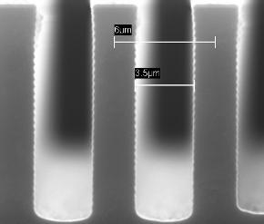
5 Device Configuration 1D PBG structure 3 silicon bar mirrors and a cavity Fabry Perot Dimensions ~2µm thick x 25µm deep Lensed Fiber Light beam 150µm 5 λ 2 4n L n 21 4n H λ 2 L Oxide λ Silicon Air Lensed Fiber Collimating Lensed fibers 9µm radius Gaussian beam 200µm Alignment grooves & springs created with an additional etch step Tuning by varying the centre cavity width Alignment Springs Filter 5
6 Optical Analysis The ideal case Transfer matrix formulation M ( λφ, ).. φ.. nh. dl... nl = nh nl..... ( λφ, ) ( λφ, ), ( λφ, ) M r t Gaussian beam input Plane wave expansion of Gaussian beam using spatial Fourier transform ( ) ( ) ixk kx E λφ, = E λ, x e dx, sinφ= k Mode overlap integral with the exit fiber 2 E out, E fiber η ( λ ) =, E1, E2 E1E2 dφ E, E E, E = φ out out fiber fiber n L r 1,t 1 (λ,φ) n H m air ¼λ c m gap ½λ c m si ¼λ c 6
7 Optical Analysis The ideal case Collimation decreases losses Loss [db] Gaussian Beam Width 4 µm 9 µm 31 µm Thin layers m=[1 1 1] Thick layers m=[21 5 2] Layer thickness effects losses and pass band Optical communication systems need narrow pass bands ~100GHz 4 si layers -30 m=[1 1 1] Freq [THz] 7
8 Optical Analysis The non-ideal case Due to imperfect deep etching, angles are introduced Fabry-Perot cavity analysis for a wedged cavity with a PBG mirror on either side ~ E out ~ p 1 2 p2 [ 2 q2 1 q1 ] i klp 2 i k ( Lq 2 + Lq1 ) ( λ, φ) = E ( λ, φ) t ( λ, φ) t ( λ, φ ) e r ( λ, φ ) r ( λ, φ ) e in 1 p= 0 q= 0 r 1,t 1 (λ,φ) ϑ r 2,t 2 (λ,φ) L 01 φ L p2 L p1 m air ¼λ c m gap ½λ c m si ¼λ c 8
9 Optical Analysis The non-ideal case Simulation for an 9µm Gaussian beam with different etching angles 0-10 Angle [deg] Ripples appear at high frequencies Loss [db] Above >0.001 deg we get excess loss and pass band widening Freq [THz] vertical etching! 9
10 Fabrication Deep Reactive Ion Etching (DRIE): Suitable for all silicon orientations Scalloping and 1-2 deg sidewall angle. KOH etching in (110) silicon (Kendall 1979): Vertical etching, but limited by etch ratio between (111):(110) Smooth surfaces Not suitable for non (111) planes Depth limited by width and length DRIE followed by short KOH etching in (110) silicon: Vertical etching Smooth surfaces If kept short, does not effect too much other orientations 10
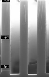
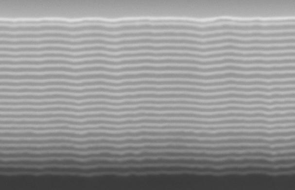
11 Fabrication 2nd DRIE etch DRIE (111) 1st etch + KOH smoothing KOH wet etching Initial scalloping DRIE + KOH 11
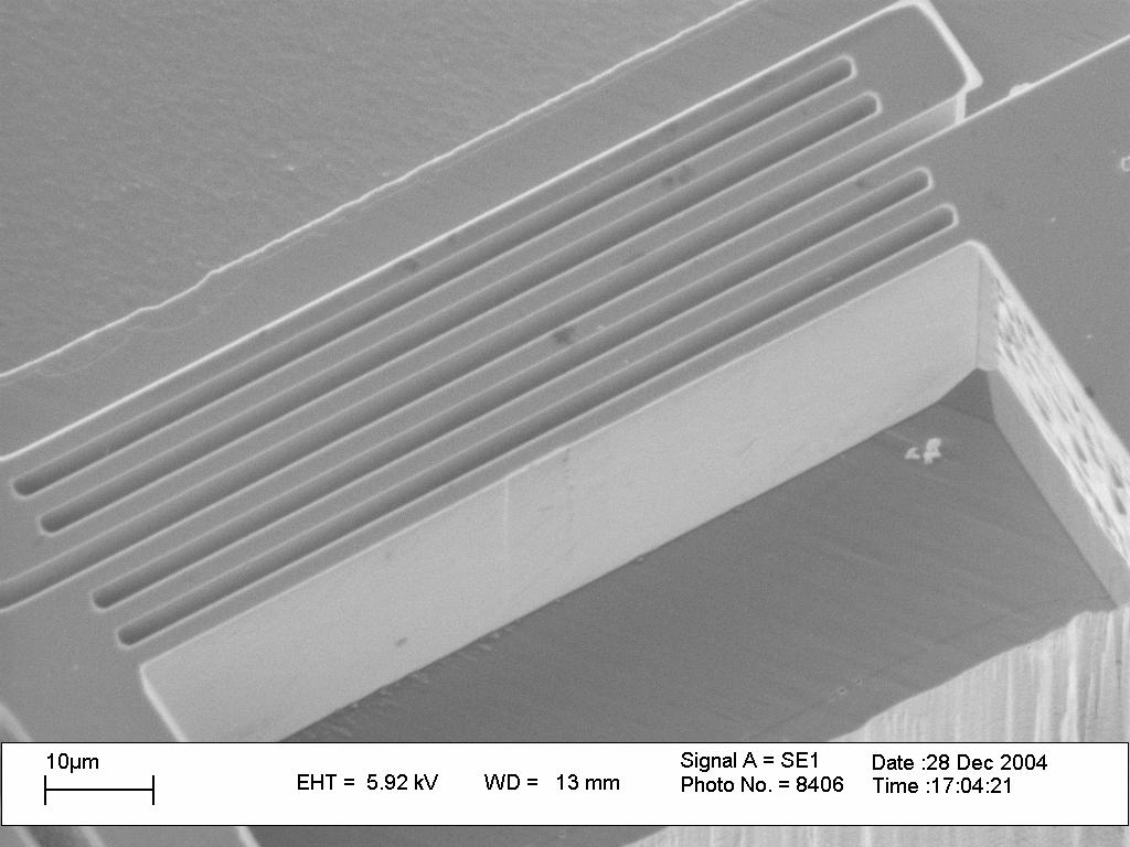
12 Fabrication Process Flow 1. Oxide + Photoresist 5. Thick Photoresist Photo resist Oxide Silicon Gold 2 DRIE 6. DRIE 3. Quick KOH dip 7. Sputter Gold 4. Oxidation + RIE 8. HF Release Fiber 12


![[deg] 0.005 0.01 Exp.](/docs-images/79/79910177/images/13-2.jpg "MEMS tuning mechanisms <0.")
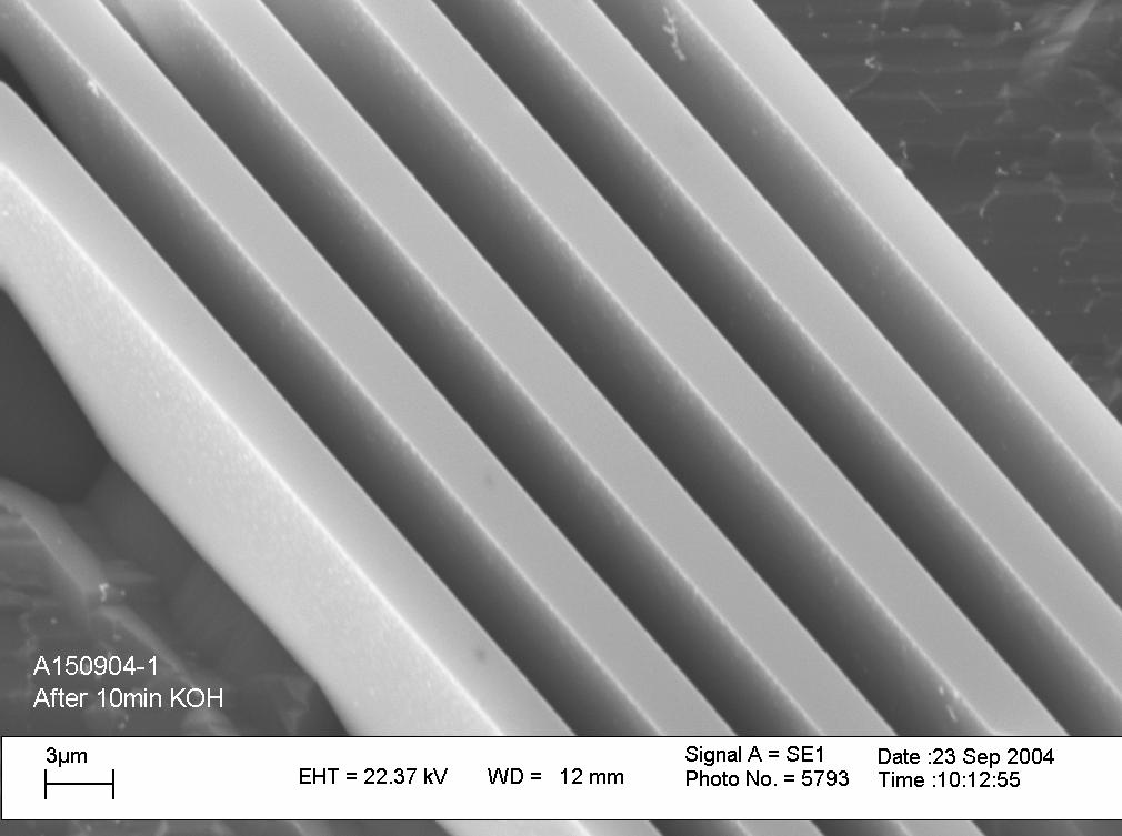
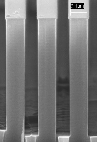
13 Fabrication Results 0.65nm pass band, -10.5dB loss and a 200Ghz channel spacing Loss [db] Angle [deg] Exp. MEMS tuning mechanisms <0.01 deg verticality Freq [THz] 13
![0 Filter Tunability +150 nm 0nm -150 nm Fabrication Tunability Loss [db] -5-10 -15-20 Mechanical movement large tuning range for the whole C & L bands ( λ=~70nm) -25 1510 1530 1550](/docs-images/79/79910177/images/14-1.jpg "1570 1590 Wavelength [nm] Use of BSOI to release moving structures: HF etched or Back etch release Downside are speed and settling time But proper design can reach µs timescales.")
14 0 Filter Tunability +150 nm 0nm -150 nm Fabrication Tunability Loss [db] Mechanical movement large tuning range for the whole C & L bands ( λ=~70nm) Wavelength [nm] Use of BSOI to release moving structures: HF etched or Back etch release Downside are speed and settling time But proper design can reach µs timescales. 14
15 Future Work Complete a tunable device Work on designs with fast response time and lower loss Reshape the band pass by passing the light twice through the cavity Loss [db] 0 1 pass 3-layers -5 1 pass 2-layers 2 pass 2-layers Freq [THz] 15
16 Summary 1D PBG filter was fabricated for DWDM networks with db fiber to fiber losses, 200 Ghz channel spacing. Combined DRIE + KOH wet etching on (110) silicon wafers for very vertical (<0.01 ) and smooth surfaces. On going work on tunability using MEMS techniques. 16
17 Acknowledgments We would like to thank the UPC, Lambdax and Coventor for their support. Thanks to Dr. John Stagg, Dr. Munir Ahmad and Michael Larsson for their kind help. Further information: 17
Study on Semiconductor Lasers of Circular Structures Fabricated by EB Lithography
 Study on Semiconductor Lasers of Circular Structures Fabricated by EB Lithography Ashim Kumar Saha (D3) Supervisor: Prof. Toshiaki Suhara Doctoral Thesis Defense Quantum Engineering Design Course Graduate
Resonator Fabrication for Cavity Enhanced, Tunable Si/Ge Quantum Cascade Detectors
 Resonator Fabrication for Cavity Enhanced, Tunable Si/Ge Quantum Cascade Detectors M. Grydlik 1, P. Rauter 1, T. Fromherz 1, G. Bauer 1, L. Diehl 2, C. Falub 2, G. Dehlinger 2, H. Sigg 2, D. Grützmacher
1. Narrative Overview Questions
 Homework 4 Due Nov. 16, 010 Required Reading: Text and Lecture Slides on Downloadable from Course WEB site: http://courses.washington.edu/overney/nme498.html 1. Narrative Overview Questions Question 1
SURFACE TENSION POWERED SELF-ASSEMBLY OF 3D MOEMS DEVICES USING DRIE OF BONDED SILICON-ON-INSULATOR WAFERS INTRODUCTION
 SURFACE TENSION POWERED SELF-ASSEMBLY OF 3D MOEMS DEVICES USING DRIE OF BONDED SILICON-ON-INSULATOR WAFERS R.R.A Syms, C. Gormley and S. Blackstone Dept. of Electrical and Electronic Engineering, Imperial
Supporting information. Unidirectional Doubly Enhanced MoS 2 Emission via
 Supporting information Unidirectional Doubly Enhanced MoS 2 Emission via Photonic Fano Resonances Xingwang Zhang, Shinhyuk Choi, Dake Wang, Carl H. Naylor, A. T. Charlie Johnson, and Ertugrul Cubukcu,,*
SUPPLEMENTARY INFORMATION
 In the format provided by the authors and unedited. DOI: 10.1038/NPHOTON.2016.254 Measurement of non-monotonic Casimir forces between silicon nanostructures Supplementary information L. Tang 1, M. Wang
MEMS Tuning-Fork Gyroscope Mid-Term Report Amanda Bristow Travis Barton Stephen Nary
 MEMS Tuning-Fork Gyroscope Mid-Term Report Amanda Bristow Travis Barton Stephen Nary Abstract MEMS based gyroscopes have gained in popularity for use as rotation rate sensors in commercial products like
EE 527 MICROFABRICATION. Lecture 25 Tai-Chang Chen University of Washington
 EE 527 MICROFABRICATION Lecture 25 Tai-Chang Chen University of Washington ION MILLING SYSTEM Kaufmann source Use e-beam to strike plasma A magnetic field applied to increase ion density Drawback Low etch
Micro Capacitive Tilt Sensor for Human Body Movement Detection
 Micro Capacitive Tilt Sensor for Human Body Movement Detection L. Zhao, E. M. Yeatman Optical and Semiconductor Devices Group, Department of Electrical & Electronic Engineering Imperial College London,
Chapter 3. Design for manufacture of Fabry-Perot cavity sensors
 Chapter 3 Design for manufacture of Fabry-Perot cavity sensors When Fabry-Perot cavity sensors are manufactured, the thickness of each layer must be tightly controlled to achieve the target performance
EE C247B / ME C218 INTRODUCTION TO MEMS DESIGN SPRING 2016 C. NGUYEN PROBLEM SET #4
 Issued: Wednesday, March 4, 2016 PROBLEM SET #4 Due: Monday, March 14, 2016, 8:00 a.m. in the EE C247B homework box near 125 Cory. 1. This problem considers bending of a simple cantilever and several methods
Dielectric Meta-Reflectarray for Broadband Linear Polarization Conversion and Optical Vortex Generation
 Supporting Information Dielectric Meta-Reflectarray for Broadband Linear Polarization Conversion and Optical Vortex Generation Yuanmu Yang, Wenyi Wang, Parikshit Moitra, Ivan I. Kravchenko, Dayrl P. Briggs,
EE 143 MICROFABRICATION TECHNOLOGY FALL 2014 C. Nguyen PROBLEM SET #7. Due: Friday, Oct. 24, 2014, 8:00 a.m. in the EE 143 homework box near 140 Cory
 Issued: Tuesday, Oct. 14, 2014 PROBLEM SET #7 Due: Friday, Oct. 24, 2014, 8:00 a.m. in the EE 143 homework box near 140 Cory Electroplating 1. Suppose you want to fabricate MEMS clamped-clamped beam structures
OPTI510R: Photonics. Khanh Kieu College of Optical Sciences, University of Arizona Meinel building R.626
 OPTI510R: Photonics Khanh Kieu College of Optical Sciences, University of Arizona kkieu@optics.arizona.edu Meinel building R.626 Important announcements Homework #1 is due. Homework #2 is assigned, due
Introduction to Microeletromechanical Systems (MEMS) Lecture 9 Topics. MEMS Overview
 Lecture 9 Topics. MEMS Overview") Introduction to Microeletromechanical Systems (MEMS) Lecture 9 Topics MicroOptoElectroMechanical Systems (MOEMS) Grating Light Valves Corner Cube Reflector (CCR) MEMS Light Modulator Optical Switch Micromirrors
Introduction to Microeletromechanical Systems (MEMS) Lecture 9 Topics MicroOptoElectroMechanical Systems (MOEMS) Grating Light Valves Corner Cube Reflector (CCR) MEMS Light Modulator Optical Switch Micromirrors
My Research. Adam Rosowski. Photonic in Engineering GROUP
 My Research Adam Rosowski Photonic in Engineering Photo onic in Engineering Motivation Chemical etching process Direct laser process HCL Technology Therahertz spectroskopy Physics Motivation Photonic in
EE C245 ME C218 Introduction to MEMS Design Fall 2007
 EE C245 ME C218 Introduction to MEMS Design Fall 2007 Prof. Clark T.-C. Nguyen Dept. of Electrical Engineering & Computer Sciences University of California at Berkeley Berkeley, CA 94720 Lecture 11: Bulk
MSN551 LITHOGRAPHY II
 MSN551 Introduction to Micro and Nano Fabrication LITHOGRAPHY II E-Beam, Focused Ion Beam and Soft Lithography Why need electron beam lithography? Smaller features are required By electronics industry:
EE 472 Solutions to some chapter 4 problems
 EE 472 Solutions to some chapter 4 problems 4.4. Erbium doped fiber amplifier An EDFA is pumped at 1480 nm. N1 and N2 are the concentrations of Er 3+ at the levels E 1 and E 2 respectively as shown in
Regents of the University of California
 Deep Reactive-Ion Etching (DRIE) DRIE Issues: Etch Rate Variance The Bosch process: Inductively-coupled plasma Etch Rate: 1.5-4 μm/min Two main cycles in the etch: Etch cycle (5-15 s): SF 6 (SF x+ ) etches
GRATING CLASSIFICATION
 GRATING CLASSIFICATION SURFACE-RELIEF GRATING TYPES GRATING CLASSIFICATION Transmission or Reflection Classification based on Regime DIFFRACTION BY GRATINGS Acousto-Optics Diffractive Optics Integrated
EE C245 ME C218 Introduction to MEMS Design Fall 2007
 EE C245 ME C218 Introduction to MEMS Design Fall 2007 Prof. Clark T.-C. Nguyen Dept. of Electrical Engineering & Computer Sciences University of California at Berkeley Berkeley, CA 94720 Lecture 12: Mechanics
Astronomical frequency comb for calibration of low and medium resolution spectrographs
 Astronomical frequency comb for calibration of low and medium resolution spectrographs innofspec at AIP has several years expertise in astronomical instrumentation. innofspec succesfully developed a new
b. The displacement of the mass due to a constant acceleration a is x=
 EE147/247A Final, Fall 2013 Page 1 /35 2 /55 NO CALCULATORS, CELL PHONES, or other electronics allowed. Show your work, and put final answers in the boxes provided. Use proper units in all answers. 1.
Edward S. Rogers Sr. Department of Electrical and Computer Engineering. ECE318S Fundamentals of Optics. Final Exam. April 16, 2007.
 Edward S. Rogers Sr. Department of Electrical and Computer Engineering ECE318S Fundamentals of Optics Final Exam April 16, 2007 Exam Type: D (Close-book + two double-sided aid sheets + a non-programmable
Understanding Semiconductor Lasers
 27 April 2010 age 1 of 8 Experiment II Understanding Semiconductor Lasers The purpose of this experiment is to explore the basic characteristics of semiconductor lasers. We will measure and calculate the
Progress In Electromagnetics Research Letters, Vol. 33, 27 35, 2012
 Progress In Electromagnetics Research Letters, Vol. 33, 27 35, 2012 TUNABLE WAVELENGTH DEMULTIPLEXER FOR DWDM APPLICATION USING 1-D PHOTONIC CRYSTAL A. Kumar 1, B. Suthar 2, *, V. Kumar 3, Kh. S. Singh
4FNJDPOEVDUPS 'BCSJDBUJPO &UDI
 2010.5.4 1 Major Fabrication Steps in CMOS Process Flow UV light oxygen Silicon dioxide Silicon substrate Oxidation (Field oxide) photoresist Photoresist Coating Mask exposed photoresist Mask-Wafer Exposed
Lecture 23 Optical MEMS (5)
") EEL6935 Advanced MEMS (Spring 2005) Instructor: Dr. Huikai Xie Lecture 23 Optical MEMS (5) Agenda: Microlenses Diffractive Microgratings Example Devices Reference: S. Sinzinger and J. Jahns, Chapter 6
EEL6935 Advanced MEMS (Spring 2005) Instructor: Dr. Huikai Xie Lecture 23 Optical MEMS (5) Agenda: Microlenses Diffractive Microgratings Example Devices Reference: S. Sinzinger and J. Jahns, Chapter 6
UNIVERSITY OF CALIFORNIA. College of Engineering. Department of Electrical Engineering and Computer Sciences. Professor Ali Javey.
 UNIVERSITY OF CALIFORNIA College of Engineering Department of Electrical Engineering and Computer Sciences EE 143 Professor Ali Javey Spring 2009 Exam 2 Name: SID: Closed book. One sheet of notes is allowed.
Self-Phase Modulation in Optical Fiber Communications: Good or Bad?
 1/100 Self-Phase Modulation in Optical Fiber Communications: Good or Bad? Govind P. Agrawal Institute of Optics University of Rochester Rochester, NY 14627 c 2007 G. P. Agrawal Outline Historical Introduction
E SC 412 Nanotechnology: Materials, Infrastructure, and Safety Wook Jun Nam
 E SC 412 Nanotechnology: Materials, Infrastructure, and Safety Wook Jun Nam Lecture 10 Outline 1. Wet Etching/Vapor Phase Etching 2. Dry Etching DC/RF Plasma Plasma Reactors Materials/Gases Etching Parameters
SUPPLEMENTARY NOTES Supplementary Note 1: Fabrication of Scanning Thermal Microscopy Probes
 SUPPLEMENTARY NOTES Supplementary Note 1: Fabrication of Scanning Thermal Microscopy Probes Fabrication of the scanning thermal microscopy (SThM) probes is summarized in Supplementary Fig. 1 and proceeds
Deformable MEMS grating for wide tunability and high operating speed
 Deformable MEMS grating for wide tunability and high operating speed Maurizio Tormen (1), Yves-Alain Peter (2), Philippe Niedermann (1), Arno Hoogerwerf (1), Herbert Shea (3) and Ross Stanley (1) 1 Centre
Ultra-narrow-band tunable laserline notch filter
 Appl Phys B (2009) 95: 597 601 DOI 10.1007/s00340-009-3447-6 Ultra-narrow-band tunable laserline notch filter C. Moser F. Havermeyer Received: 5 December 2008 / Revised version: 2 February 2009 / Published
EECS C245 ME C218 Midterm Exam
 University of California at Berkeley College of Engineering EECS C245 ME C218 Midterm Eam Fall 2003 Prof. Roger T. Howe October 15, 2003 Dr. Thara Srinivasan Guidelines Your name: SOLUTIONS Circle your
>> D-5006 CWDM components for 40 G and 100 G Transceivers
 >> D-5006 CWDM components for 40 G and 100 G Transceivers Introduction In this White paper the principals of Cube s Thin Film Filter design and their performance with regard to construction tolerances
ECE 484 Semiconductor Lasers
 ECE 484 Semiconductor Lasers Dr. Lukas Chrostowski Department of Electrical and Computer Engineering University of British Columbia January, 2013 Module Learning Objectives: Understand the importance of
Development and Characterization of High Frequency Bulk Mode Resonators
 Excerpt from the Proceedings of the COMSOL Conference 008 Hannover Development and Characterization of High Frequency Bulk Mode Resonators Hossein Pakdast 1*, Zachary James Davis 1 1 DTU Nanotech, Technical
UNIVERSITY OF CALIFORNIA College of Engineering Department of Electrical Engineering and Computer Sciences. Professor Chenming Hu.
 UNIVERSITY OF CALIFORNIA College of Engineering Department of Electrical Engineering and Computer Sciences EECS 130 Spring 2009 Professor Chenming Hu Midterm I Name: Closed book. One sheet of notes is
Micro- and Nano-Technology... for Optics
 Micro- and Nano-Technology...... for Optics U.D. Zeitner Fraunhofer Institut für Angewandte Optik und Feinmechanik Jena Today: 1. Introduction E. Bernhard Kley Institute of Applied Physics Friedrich-Schiller
Refractive Index Measurement by Gain- or Loss-Induced Resonance
 Refractive Index Measurement by Gain- or Loss-Induced Resonance 59 Refractive Index Measurement by Gain- or Loss-Induced Resonance Markus Miller Using a semiconductor optical resonator consisting of a
UNIT 3. By: Ajay Kumar Gautam Asst. Prof. Dev Bhoomi Institute of Technology & Engineering, Dehradun
 UNIT 3 By: Ajay Kumar Gautam Asst. Prof. Dev Bhoomi Institute of Technology & Engineering, Dehradun 1 Syllabus Lithography: photolithography and pattern transfer, Optical and non optical lithography, electron,
Wet and Dry Etching. Theory
 Wet and Dry Etching Theory 1. Introduction Etching techniques are commonly used in the fabrication processes of semiconductor devices to remove selected layers for the purposes of pattern transfer, wafer
DESIGN AND FABRICATION OF THE MICRO- ACCELEROMETER USING PIEZOELECTRIC THIN FILMS
 DESIGN AND FABRICATION OF THE MICRO- ACCELEROMETER USING PIEZOELECTRIC THIN FILMS JYH-CHENG YU and FU-HSIN LAI Department of Mechanical Engineering National Taiwan University of Science and Technology
Supplementary Figure 1: Reflectivity under continuous wave excitation.
 SUPPLEMENTARY FIGURE 1 Supplementary Figure 1: Reflectivity under continuous wave excitation. Reflectivity spectra and relative fitting measured for a bias where the QD exciton transition is detuned from
CHARACTERIZATION OF DEEP REACTIVE ION ETCHING (DRIE) PROCESS FOR ELECTRICAL THROUGH-WAFER INTERCONNECTS FOR PIEZORESISTIVE INERTIAL SENSORS
 PROCESS FOR ELECTRICAL THROUGH-WAFER INTERCONNECTS FOR PIEZORESISTIVE INERTIAL SENSORS") CHARACTERIZATION OF DEEP REACTIVE ION ETCHING (DRIE) PROCESS FOR ELECTRICAL THROUGH-WAFER INTERCONNECTS FOR PIEZORESISTIVE INERTIAL SENSORS Maria Suggs, Physics Major, Southern Polytechnic State University
CHARACTERIZATION OF DEEP REACTIVE ION ETCHING (DRIE) PROCESS FOR ELECTRICAL THROUGH-WAFER INTERCONNECTS FOR PIEZORESISTIVE INERTIAL SENSORS Maria Suggs, Physics Major, Southern Polytechnic State University
Laser Types Two main types depending on time operation Continuous Wave (CW) Pulsed operation Pulsed is easier, CW more useful
 Pulsed operation Pulsed is easier, CW more useful") Main Requirements of the Laser Optical Resonator Cavity Laser Gain Medium of 2, 3 or 4 level types in the Cavity Sufficient means of Excitation (called pumping) eg. light, current, chemical reaction Population
Main Requirements of the Laser Optical Resonator Cavity Laser Gain Medium of 2, 3 or 4 level types in the Cavity Sufficient means of Excitation (called pumping) eg. light, current, chemical reaction Population
EE C245 / ME C218 INTRODUCTION TO MEMS DESIGN FALL 2009 PROBLEM SET #7. Due (at 7 p.m.): Thursday, Dec. 10, 2009, in the EE C245 HW box in 240 Cory.
: Thursday, Dec. 10, 2009, in the EE C245 HW box in 240 Cory.") Issued: Thursday, Nov. 24, 2009 PROBLEM SET #7 Due (at 7 p.m.): Thursday, Dec. 10, 2009, in the EE C245 HW box in 240 Cory. 1. Gyroscopes are inertial sensors that measure rotation rate, which is an extremely
Issued: Thursday, Nov. 24, 2009 PROBLEM SET #7 Due (at 7 p.m.): Thursday, Dec. 10, 2009, in the EE C245 HW box in 240 Cory. 1. Gyroscopes are inertial sensors that measure rotation rate, which is an extremely
Chemistry Instrumental Analysis Lecture 5. Chem 4631
 Chemistry 4631 Instrumental Analysis Lecture 5 Light Amplification by Stimulated Emission of Radiation High Intensities Narrow Bandwidths Coherent Outputs Applications CD/DVD Readers Fiber Optics Spectroscopy
Fabrication Technology, Part I
 EEL5225: Principles of MEMS Transducers (Fall 2004) Fabrication Technology, Part I Agenda: Microfabrication Overview Basic semiconductor devices Materials Key processes Oxidation Thin-film Deposition Reading:
U-Shaped Nano-Apertures for Enhanced Optical Transmission and Resolution
 U-Shaped Nano-Apertures for Enhanced Optical Transmission and Resolution Mustafa Turkmen 1,2,3, Serap Aksu 3,4, A. Engin Çetin 2,3, Ahmet A. Yanik 2,3, Alp Artar 2,3, Hatice Altug 2,3,4, * 1 Electrical
Blue-green Emitting Semiconductor Disk Lasers with Intra-Cavity Frequency Doubling
 Blue-green Emitting Semiconductor Disk Lasers with Intra-Cavity Frequency Doubling Eckart Schiehlen and Michael Riedl Diode-pumped semiconductor disk lasers, also referred to as VECSEL (Vertical External
Alignment of Liquid Crystals by Ion Etched Grooved Glass Surfaces. Yea-Feng Lin, Ming-Chao Tsou, and Ru-Pin Pan
 CHINESE JOURNAL OF PHYSICS VOL. 43, NO. 6 DECEMBER 2005 Alignment of Liquid Crystals by Ion Etched Grooved Glass Surfaces Yea-Feng Lin, Ming-Chao Tsou, and Ru-Pin Pan Department of Electrophysics, National
Optimum Access Waveguide Width for 1xN Multimode. Interference Couplers on Silicon Nanomembrane
 Optimum Access Waveguide Width for 1xN Multimode Interference Couplers on Silicon Nanomembrane Amir Hosseini 1,*, Harish Subbaraman 2, David Kwong 1, Yang Zhang 1, and Ray T. Chen 1,* 1 Microelectronic
Nanomaterials and their Optical Applications
 Nanomaterials and their Optical Applications Winter Semester 2012 Lecture 08 rachel.grange@uni-jena.de http://www.iap.uni-jena.de/multiphoton Outline: Photonic crystals 2 1. Photonic crystals vs electronic
Supplementary Methods A. Sample fabrication
 Supplementary Methods A. Sample fabrication Supplementary Figure 1(a) shows the SEM photograph of a typical sample, with three suspended graphene resonators in an array. The cross-section schematic is
Second-Harmonic Generation Studies of Silicon Interfaces
 Second-Harmonic Generation Studies of Silicon Interfaces Z. Marka 1, Y. D. Glinka 1, Y. Shirokaya 1, M. Barry 1, S. N. Rashkeev 1, W. Wang 1, R. D. Schrimpf 2,D. M. Fleetwood 2 and N. H. Tolk 1 1 Department
SUPPLEMENTARY FIGURES
 SUPPLEMENTARY FIGURES a b c Supplementary Figure 1 Fabrication of the near-field radiative heat transfer device. a, Main fabrication steps for the bottom Si substrate. b, Main fabrication steps for the
Supplementary Information Our InGaN/GaN multiple quantum wells (MQWs) based one-dimensional (1D) grating structures
 based one-dimensional (1D) grating structures") Polarized white light from hybrid organic/iii-nitrides grating structures M. Athanasiou, R. M. Smith, S. Ghataora and T. Wang* Department of Electronic and Electrical Engineering, University of Sheffield,
Polarized white light from hybrid organic/iii-nitrides grating structures M. Athanasiou, R. M. Smith, S. Ghataora and T. Wang* Department of Electronic and Electrical Engineering, University of Sheffield,
Etching: Basic Terminology
 Lecture 7 Etching Etching: Basic Terminology Introduction : Etching of thin films and sometimes the silicon substrate are very common process steps. Usually selectivity, and directionality are the first
SUPPLEMENTARY INFORMATION
 SUPPLEMENTARY INFORMATION Supplementary Information I. Schematic representation of the zero- n superlattices Schematic representation of a superlattice with 3 superperiods is shown in Fig. S1. The superlattice
Lecture 18: Microfluidic MEMS, Applications
 MECH 466 Microelectromechanical Systems University of Victoria Dept. of Mechanical Engineering Lecture 18: Microfluidic MEMS, Applications 1 Overview Microfluidic Electrokinetic Flow Basic Microfluidic
EE-612: Lecture 22: CMOS Process Steps
 EE-612: Lecture 22: CMOS Process Steps Mark Lundstrom Electrical and Computer Engineering Purdue University West Lafayette, IN USA Fall 2006 NCN www.nanohub.org Lundstrom EE-612 F06 1 outline 1) Unit Process
Figure 1: Graphene release, transfer and stacking processes. The graphene stacking began with CVD
 Supplementary figure 1 Graphene Growth and Transfer Graphene PMMA FeCl 3 DI water Copper foil CVD growth Back side etch PMMA coating Copper etch in 0.25M FeCl 3 DI water rinse 1 st transfer DI water 1:10
Surface plasmon waveguides
 Surface plasmon waveguides Introduction Size Mismatch between Scaled CMOS Electronics and Planar Photonics Photonic integrated system with subwavelength scale components CMOS transistor: Medium-sized molecule
produced a sputter rate of 0.9 nm/s for the radially profiled, un-etched wires. A slightly
 Supporting Information: Beam Current and Sputtering Rate: Using a 16 kev Cs + primary ion beam and a 1 µm 2 rastered area, a 10 pa beam current produced a sputter rate of 0.9 nm/s for the radially profiled,
Edward S. Rogers Sr. Department of Electrical and Computer Engineering. ECE426F Optical Engineering. Final Exam. Dec. 17, 2003.
 Edward S. Rogers Sr. Department of Electrical and Computer Engineering ECE426F Optical Engineering Final Exam Dec. 17, 2003 Exam Type: D (Close-book + one 2-sided aid sheet + a non-programmable calculator)
Integrating MEMS Electro-Static Driven Micro-Probe and Laser Doppler Vibrometer for Non-Contact Vibration Mode SPM System Design
 Tamkang Journal of Science and Engineering, Vol. 12, No. 4, pp. 399 407 (2009) 399 Integrating MEMS Electro-Static Driven Micro-Probe and Laser Doppler Vibrometer for Non-Contact Vibration Mode SPM System
Modelling of temperature profiles in Nd:YAG laser annealed GaAs/AlGaAs quantum well microstructures
 Modelling of temperature profiles in Nd:YG laser annealed Gas/lGas quantum well microstructures Radoslaw Stanowski Ph.D. O. Voznyy prof. J J. Dubowski 1 Outline 1. Motivation 2. Transient temperature analysis
= nm. = nm. = nm
 Chemistry 60 Analytical Spectroscopy PROBLEM SET 5: Due 03/0/08 1. At a recent birthday party, a young friend (elementary school) noticed that multicolored rings form across the surface of soap bubbles.
Oscillateur paramétrique optique en
 C. Ozanam 1, X. Lafosse 2, I. Favero 1, S. Ducci 1, G. Leo 1 1 Université Paris Diderot, Sorbonne Paris Cité, Laboratoire MPQ, CNRS-UMR 7162, Paris, France, 2 Laboratoire de Photonique et Nanostructures,
Some Topics in Optics
 Some Topics in Optics The HeNe LASER The index of refraction and dispersion Interference The Michelson Interferometer Diffraction Wavemeter Fabry-Pérot Etalon and Interferometer The Helium Neon LASER A
Principles of Mode-Hop Free Wavelength Tuning
 Principles of Mode-Hop Free Wavelength Tuning Table of Contents 1. Introduction... 2 2. Tunable Diode Lasers in Littrow Cavity Design... 5 2.1 Pivot Point Requirements... 5 2.2 Realization according to
EE C245 ME C218 Introduction to MEMS Design
 EE C245 ME C218 Introduction to MEMS Design Fall 2007 Prof. Clark T.-C. Nguyen Dept. of Electrical Engineering & Computer Sciences University of California at Berkeley Berkeley, CA 94720 Lecture 21: Gyros
3.1 Absorption and Transparency
 3.1 Absorption and Transparency 3.1.1 Optical Devices (definitions) 3.1.2 Photon and Semiconductor Interactions 3.1.3 Photon Intensity 3.1.4 Absorption 3.1 Absorption and Transparency Objective 1: Recall
The Stanford Nanofabrication Facility. Etch Area Overview. May 21, 2013
 The Stanford Nanofabrication Facility Etch Area Overview May 21, 2013 High Density Plasma Systems Etcher Materials Etched Gases available Wafer Size Applied Materials P5000 MRIE ChA Applied Materials P5000
Lecture 0: Introduction
 Lecture 0: Introduction Introduction q Integrated circuits: many transistors on one chip q Very Large Scale Integration (VLSI): bucketloads! q Complementary Metal Oxide Semiconductor Fast, cheap, low power
CBSE PHYSICS QUESTION PAPER (2005)
") CBSE PHYSICS QUESTION PAPER (2005) (i) (ii) All questions are compulsory. There are 30 questions in total. Questions 1 to 8 carry one mark each, Questions 9 to 18 carry two marks each, Question 19 to 27
CBSE PHYSICS QUESTION PAPER (2005) (i) (ii) All questions are compulsory. There are 30 questions in total. Questions 1 to 8 carry one mark each, Questions 9 to 18 carry two marks each, Question 19 to 27
What Makes a Laser Light Amplification by Stimulated Emission of Radiation Main Requirements of the Laser Laser Gain Medium (provides the light
 What Makes a Laser Light Amplification by Stimulated Emission of Radiation Main Requirements of the Laser Laser Gain Medium (provides the light amplification) Optical Resonator Cavity (greatly increase
Tunable GaN-Based Laser Diode
 Tunable GaN-Based Laser Diode Christoph Eichler We have investigated the wavelength tuning characteristics of a GaN-based cw-laser diode with an emission wavelength of 425 nm. Temperature dependent spectra
Well resolved measurements of turbulent fluxes in the atmospheric surface layer
 Well resolved measurements of turbulent fluxes in the atmospheric surface layer M. Hultmark, G. Arwatz, M. Vallikivi, Y. Fan and C. Bahri Princeton University Department of Mechanical and Aerospace Engineering
Chapter-4 Stimulated emission devices LASERS
 Semiconductor Laser Diodes Chapter-4 Stimulated emission devices LASERS The Road Ahead Lasers Basic Principles Applications Gas Lasers Semiconductor Lasers Semiconductor Lasers in Optical Networks Improvement
Where are the Fringes? (in a real system) Div. of Amplitude - Wedged Plates. Fringe Localisation Double Slit. Fringe Localisation Grating
 Div. of Amplitude - Wedged Plates. Fringe Localisation Double Slit. Fringe Localisation Grating") Where are the Fringes? (in a real system) Fringe Localisation Double Slit spatial modulation transverse fringes? everywhere or well localised? affected by source properties: coherence, extension Plane
Where are the Fringes? (in a real system) Fringe Localisation Double Slit spatial modulation transverse fringes? everywhere or well localised? affected by source properties: coherence, extension Plane
Fabrication and optical measurements of silicon on insulator photonic nanostructures
 Microelectronic Engineering 61 62 (2002) 529 536 www.elsevier.com/ locate/ mee Fabrication and optical measurements of silicon on insulator photonic nanostructures * M. Agio, L.C. Andreani, E. Silberstein,
Section 3: Etching. Jaeger Chapter 2 Reader
 Section 3: Etching Jaeger Chapter 2 Reader Etch rate Etch Process - Figures of Merit Etch rate uniformity Selectivity Anisotropy d m Bias and anisotropy etching mask h f substrate d f d m substrate d f
Midterm I - Solutions
 UNIVERSITY OF CALIFORNIA College of Engineering Department of Electrical Engineering and Computer Sciences EECS 130 Spring 2008 Professor Chenming Hu Midterm I - Solutions Name: SID: Grad/Undergrad: Closed
Refraction and Dispersion in Nonlinear Photonic Crystal Superlattices
 Refraction and Dispersion in Nonlinear Photonic Crystal Superlattices LEOS 18 th Annual Meeting Sydney, Australia Monday, 24 October 2005 Curtis W. Neff, Tsuyoshi Yamashita and Christopher J. Summers Presented
A Micromechanical Red-Shifting Tunable Vertical Cavity Filter. Steven Michael Chase. B.S. (California Institute of Technology) 1997
 1997") A Micromechanical Red-Shifting Tunable Vertical Cavity Filter by Steven Michael Chase B.S. (California Institute of Technology) 1997 A thesis submitted in partial satisfaction of the requirements for the
A Micromechanical Red-Shifting Tunable Vertical Cavity Filter by Steven Michael Chase B.S. (California Institute of Technology) 1997 A thesis submitted in partial satisfaction of the requirements for the
EE C245 ME C218 Introduction to MEMS Design Fall 2010
 Lecture Outline EE C245 ME C28 Introduction to MEMS Design Fall 200 Prof. Clark T.-C. Nguyen Dept. of Electrical Engineering & Computer Sciences University of California at Berkeley Berkeley, CA 94720
Nanostructures Fabrication Methods
 Nanostructures Fabrication Methods bottom-up methods ( atom by atom ) In the bottom-up approach, atoms, molecules and even nanoparticles themselves can be used as the building blocks for the creation of
Reactive Ion Etching (RIE)
") Reactive Ion Etching (RIE) RF 13.56 ~ MHz plasma Parallel-Plate Reactor wafers Sputtering Plasma generates (1) Ions (2) Activated neutrals Enhance chemical reaction 1 2 Remote Plasma Reactors Plasma Sources
Reactive Ion Etching (RIE) RF 13.56 ~ MHz plasma Parallel-Plate Reactor wafers Sputtering Plasma generates (1) Ions (2) Activated neutrals Enhance chemical reaction 1 2 Remote Plasma Reactors Plasma Sources
Resonant terahertz absorption by plasmons in grating-gate GaN HEMT structures
 Resonant terahertz absorption by plasmons in grating-gate GaN HEMT structures A.V. Muravjov* a, D.B. Veksler a, X. Hu b, R. Gaska b, N. Pala c, H. Saxena d, R.E. Peale d, M.S. Shur a a ECSE Department,
Laser Types Two main types depending on time operation Continuous Wave (CW) Pulsed operation Pulsed is easier, CW more useful
 Pulsed operation Pulsed is easier, CW more useful") What Makes a Laser Light Amplification by Stimulated Emission of Radiation Main Requirements of the Laser Laser Gain Medium (provides the light amplification) Optical Resonator Cavity (greatly increase
What Makes a Laser Light Amplification by Stimulated Emission of Radiation Main Requirements of the Laser Laser Gain Medium (provides the light amplification) Optical Resonator Cavity (greatly increase
REFRACTORY METAL OXIDES: FABRICATION OF NANOSTRUCTURES, PROPERTIES AND APPLICATIONS
 REFRACTORY METAL OXIDES: FABRICATION OF NANOSTRUCTURES, PROPERTIES AND APPLICATIONS S.K. Lazarouk, D.A. Sasinovich BELARUSIAN STATE UNIVERSITY OF INFORMATICS AND RADIOELECTRONICS Outline: -- experimental
Infrastructure of Thin Films Laboratory in Institute of Molecular Physics Polish Academy of Sciences
 Infrastructure of Thin Films Laboratory in Institute of Molecular Physics Polish Academy of Sciences Outline Sample preparation Magnetron sputtering Ion-beam sputtering Pulsed laser deposition Electron-beam
S. Blair September 27,
 S. Blair September 7, 010 54 4.3. Optical Resonators With Spherical Mirrors Laser resonators have the same characteristics as Fabry-Perot etalons. A laser resonator supports longitudinal modes of a discrete
UNIVERSITY OF CALIFORNIA College of Engineering Department of Electrical Engineering and Computer Sciences. Professor Ali Javey. Fall 2009.
 UNIVERSITY OF CALIFORNIA College of Engineering Department of Electrical Engineering and Computer Sciences EE143 Professor Ali Javey Fall 2009 Exam 1 Name: SID: Closed book. One sheet of notes is allowed.
Signal regeneration - optical amplifiers
 Signal regeneration - optical amplifiers In any atom or solid, the state of the electrons can change by: 1) Stimulated absorption - in the presence of a light wave, a photon is absorbed, the electron is
Appendix. Photonic crystal lasers: future integrated devices
 91 Appendix Photonic crystal lasers: future integrated devices 5.1 Introduction The technology of photonic crystals has produced a large variety of new devices. However, photonic crystals have not been