III V Semiconductor Etching Process Quality Rather Than Quantity. Alan Webb. (formally of Plessey, GEC, Marconi, Bookham, Oclaro etc...
|
|
|
- Junior Hensley
- 6 years ago
- Views:
Transcription
1 III V Semiconductor Etching Process Quality Rather Than Quantity Alan Webb (formally of Plessey, GEC, Marconi, Bookham, Oclaro etc... ) Wednesday 12 th October 2016 Ricoh Arena, Coventry, UK Part of The 7 th Vacuum Symposium UK
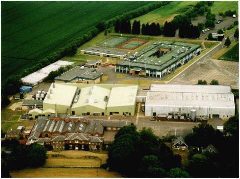
2 Caswell, Northamptonshire

3 Caswell Science and Technology Park
4 Optoelectronics Lasers Modulators Amplifiers Detectors


5 Laser Fabrication 3 wafer: ~2500 die Plan view of chip Completed Laser Chip Bar Cleave / Facet coating Wafer Thinning Metal Deposition Etch & Dep Tools Cross section of Ridge Photolithography Dielectric Deposition & Etch Bare Wafer Gratings fabrication MOVPE Overgrowth MOVPE Reactor Photolithography Tracks MOVPE Growth (2stages) Purchased bare wafer

6 A Bonded Chip
7 III V Dry Etching GaInAsP material system grown on InP Halogens : eg. Cl Br I or CH 4 / H 2
8 Developing the Process It is difficult to develop a process progressing through several different material structures and maintain complete control. It is even more difficult with the restraint of the peripheral architecture on the rest of the wafer. However, it can be done.

9 HBr Test Structure
10 HBr Ridge Etch

11 Cl 2 / N 2 Etch
12


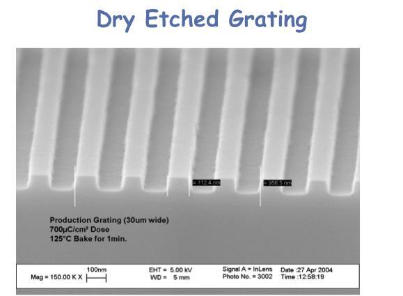
13 Grating Fabrication Low power oxygen RIE to de-scum AFM used to assess mark space ratio prior to etch Target mark/space is 1±0.3

14 TEM micrograph showing an overgrown DFB laser grating (grating period ~240nm)
15 Dry Etch Requirements Gentle Precise Controllable Physical + chemical Methane (CH 4 ) + Hydrogen (H 2 )
16 Etch Mechanism Etching and Deposition Polymer formation Polymer removal Gas mixture critical Elimination of residuals Vacuum quality
17 CH 4 + H 2 Large amount of H 2 to initiate breakdown Cracking of CH 4 results in polymer Contamination control Vacuum quality Low power plasma dimension control
18 Processes to Consider Simplified with no other interference!!! O 2 RIE 4C + 3O 2 2CO 2 + 2CO CH 3 + 2C + 3O 2 H 2 O + OH + 2CO 2 + 2CO The III V semiconductor reaction : InP + CH 4 + H 2 methyl / ethyl (Gp III) + PH 3 InP + 3CH 4 + H 2 In(CH 3 ) 3 + PH 3 + H 2 GaAs etc
19 Residual Gases The number of unwanted atoms and molecules within the environment can have a detrimental effect on dry processing. Both gas phase and surface effects can occur, which produce unwanted results. Poor quality etching could be the result.
20 Contamination Control Unwanted Reactions OH H 2 O O O 2 CO Monitor N 2 and Ar
21 In Situ Monitoring
22 Mass Spectrometry Raw Data High resolution Mass Scan High Resolution Mass Scan 1.00E-06 residual gases - air leak 1.00E-07 pp 1.00E E m / q
23 Species to Monitor? Species Mass H H 2 CH O O CH 3 COH SiH OH H 2 O CO CO 2 SiO Ar 40
24 Species to Monitor? Dominant species from etchant or reactions or important species to realise precise control? Are they the same?
25 In-situ Process Monitoring 1.00E-05 Polymer removal B412 # E-06 mtorr 1.00E E-08 H H2 He CH3 O OH H2O CO COH O2 Ar CO2 1.00E Time (mins)
26 In Situ Plasma Monitoring 1.00E-05 Polymer Removal (O2 RIE) 1.00E-06 Signal 1.00E E E Time (mins)
27 A Methane (CH4) Hydrogen (H2) Etch Process In - situ Process Monitoring 1.00E E-06 H2 O2 H H2 P H He CH3 CH4 / O 1.00E-07 CH4 CH3 O OH H2O N2 / CO 1.00E-08 N2 CO CO2 H2 H COH / SiH O2 Ar / SiC CO2 / SiO 1.00E time (mins)

28 HBr Ridge Etch
29 High resolution Mass Scan HBr chemistry 1.00E-06 H H2 Bromine has 2 stable isotopes: 79Br (50.69 %) and 81Br (49.31%). single scan 1.00E-07 Br HBr I He 1.00E-08 PH PHx Br2+ HBr E E m / q
30 High resolution Mass Scan 1.00E-06 Mass scan Thurs 14th Oct 2010 H2 He j = 6 sccm 1.00E-07 Br + HBr P 1.00E-08 P (Br + HBr)2+ P2 1.00E-09 PO 1.00E m / q
31 HBr scan during process HBr chemistry - ridge etch 1.00E-06 Bromine has 2 stable isotopes: 79Br (50.69 %) and 81Br (49.31%). 1.00E-07 p single scan 1.00E E E m / q
32 Developing the Process for Manufacture Developing a process is even more difficult for reproducibility and repeatability, such that it is the same for wafer to wafer, for batch to batch, hour by hour, day by day, because that is what manufacturing demands!!!
33 HBr Batch Processing Etch process stablisation 1.00E E-06 P 1.00E E-08 H H2 He CH3 CH4 / O OH H2O CO/ N2 O2 / PH Ar Br HBr 1.00E time

34 Complex Features Realised
35 Requirements Precise control of the vacuum, residual gas and the plasma environment are all important in being able to reliably reproduce complex features within optoelectronic devices. These are the fundamental building blocks of many types of integrated chips.

36 Chip-on-tile for angled waveguide output
37 Questions?
Effect of Gas Flow Rate and Gas Composition in Ar/CH 4 Inductively Coupled Plasmas
 COMSOL CONFERENCE BOSTON 2011 Effect of Gas Flow Rate and Gas Composition in Ar/CH 4 Inductively Coupled Plasmas Keisoku Engineering System Co., Ltd., JAPAN Dr. Lizhu Tong October 14, 2011 1 Contents 1.
Section 3: Etching. Jaeger Chapter 2 Reader
 Section 3: Etching Jaeger Chapter 2 Reader Etch rate Etch Process - Figures of Merit Etch rate uniformity Selectivity Anisotropy d m Bias and anisotropy etching mask h f substrate d f d m substrate d f
Figure 1: Graphene release, transfer and stacking processes. The graphene stacking began with CVD
 Supplementary figure 1 Graphene Growth and Transfer Graphene PMMA FeCl 3 DI water Copper foil CVD growth Back side etch PMMA coating Copper etch in 0.25M FeCl 3 DI water rinse 1 st transfer DI water 1:10
Dry Etching Zheng Yang ERF 3017, MW 5:15-6:00 pm
 Dry Etching Zheng Yang ERF 3017, email: yangzhen@uic.edu, MW 5:15-6:00 pm Page 1 Page 2 Dry Etching Why dry etching? - WE is limited to pattern sizes above 3mm - WE is isotropic causing underetching -
Etching Capabilities at Harvard CNS. March 2008
 Etching Capabilities at Harvard CNS March 2008 CNS: A shared use facility for the Harvard Community and New England CNS Provides technical support, equipment and staff. Explicitly multi-disciplinary w/
SUPPLEMENTARY INFORMATION
 SUPPLEMENTARY INFORMATION Electroluminescence from a single nanotube-molecule-nanotube junction Christoph W. Marquardt, Sergio Grunder, Alfred Błaszczyk, Simone Dehm, Frank Hennrich, Hilbert v. Löhneysen,
Plasma Deposition (Overview) Lecture 1
 Lecture 1") Plasma Deposition (Overview) Lecture 1 Material Processes Plasma Processing Plasma-assisted Deposition Implantation Surface Modification Development of Plasma-based processing Microelectronics needs (fabrication
Plasma Deposition (Overview) Lecture 1 Material Processes Plasma Processing Plasma-assisted Deposition Implantation Surface Modification Development of Plasma-based processing Microelectronics needs (fabrication
4FNJDPOEVDUPS 'BCSJDBUJPO &UDI
 2010.5.4 1 Major Fabrication Steps in CMOS Process Flow UV light oxygen Silicon dioxide Silicon substrate Oxidation (Field oxide) photoresist Photoresist Coating Mask exposed photoresist Mask-Wafer Exposed
Extrel Application Note
 Extrel Application Note Real-Time Plasma Monitoring and Detection of Trace H 2 O and HF Species in an Argon Based Plasma Jian Wei, 575 Epsilon Drive, Pittsburgh, PA 15238. (Presented at the 191st Electrochemical
Defining an optimal plasma processing toolkit for Indium Phosphide (InP) laser diode production
 laser diode production") White Paper Defining an optimal plasma processing toolkit for Indium Phosphide (InP) laser diode production The properties of InP which combine a wide band gap with high electron mobility, make it a desirable
White Paper Defining an optimal plasma processing toolkit for Indium Phosphide (InP) laser diode production The properties of InP which combine a wide band gap with high electron mobility, make it a desirable
A Novel Approach to the Layer Number-Controlled and Grain Size- Controlled Growth of High Quality Graphene for Nanoelectronics
 Supporting Information A Novel Approach to the Layer Number-Controlled and Grain Size- Controlled Growth of High Quality Graphene for Nanoelectronics Tej B. Limbu 1,2, Jean C. Hernández 3, Frank Mendoza
Etching: Basic Terminology
 Lecture 7 Etching Etching: Basic Terminology Introduction : Etching of thin films and sometimes the silicon substrate are very common process steps. Usually selectivity, and directionality are the first
Supplementary Figure 1 Detailed illustration on the fabrication process of templatestripped
 Supplementary Figure 1 Detailed illustration on the fabrication process of templatestripped gold substrate. (a) Spin coating of hydrogen silsesquioxane (HSQ) resist onto the silicon substrate with a thickness
Plasma etching. Bibliography
 Plasma etching Bibliography 1. B. Chapman, Glow discharge processes, (Wiley, New York, 1980). - Classical plasma processing of etching and sputtering 2. D. M. Manos and D. L. Flamm, Plasma etching; An
UNIT 3. By: Ajay Kumar Gautam Asst. Prof. Dev Bhoomi Institute of Technology & Engineering, Dehradun
 UNIT 3 By: Ajay Kumar Gautam Asst. Prof. Dev Bhoomi Institute of Technology & Engineering, Dehradun 1 Syllabus Lithography: photolithography and pattern transfer, Optical and non optical lithography, electron,
Competitive Advantages of Ontos7 Atmospheric Plasma
 Competitive Advantages of Ontos7 Atmospheric Plasma Eric Schulte Matt Phillips Keith Cooper SETNA Proprietary 1 Advantages of Ontos7 Atmospheric Plasma Process over Vacuum RIE Plasma for Die/Wafer Surface
Supplementary Information. Rapid Stencil Mask Fabrication Enabled One-Step. Polymer-Free Graphene Patterning and Direct
 Supplementary Information Rapid Stencil Mask Fabrication Enabled One-Step Polymer-Free Graphene Patterning and Direct Transfer for Flexible Graphene Devices Keong Yong 1,, Ali Ashraf 1,, Pilgyu Kang 1,
Chapter 6. Summary and Conclusions
 Chapter 6 Summary and Conclusions Plasma deposited amorphous hydrogenated carbon films (a-c:h) still attract a lot of interest due to their extraordinary properties. Depending on the deposition conditions
Case Study of Electronic Materials Packaging with Poor Metal Adhesion and the Process for Performing Root Cause Failure Analysis
 Case Study of Electronic Materials Packaging with Poor Metal Adhesion and the Process for Performing Root Cause Failure Analysis Dr. E. A. Leone BACKGRUND ne trend in the electronic packaging industry
ETCHING Chapter 10. Mask. Photoresist
 ETCHING Chapter 10 Mask Light Deposited Substrate Photoresist Etch mask deposition Photoresist application Exposure Development Etching Resist removal Etching of thin films and sometimes the silicon substrate
CHAPTER 6: Etching. Chapter 6 1
 Chapter 6 1 CHAPTER 6: Etching Different etching processes are selected depending upon the particular material to be removed. As shown in Figure 6.1, wet chemical processes result in isotropic etching
LECTURE 5 SUMMARY OF KEY IDEAS
 LECTURE 5 SUMMARY OF KEY IDEAS Etching is a processing step following lithography: it transfers a circuit image from the photoresist to materials form which devices are made or to hard masking or sacrificial
INTRODUCTION TO THE HYBRID PLASMA EQUIPMENT MODEL
 INTRODUCTION TO THE HYBRID PLASMA EQUIPMENT MODEL Prof. Mark J. Kushner Department of Electrical and Computer Engineering 1406 W. Green St. Urbana, IL 61801 217-144-5137 mjk@uiuc.edu http://uigelz.ece.uiuc.edu
Plasma Chemistry Study in an Inductively Coupled Dielectric Etcher
 Plasma Chemistry Study in an Inductively Coupled Dielectric Etcher Chunshi Cui, John Trow, Ken Collins, Betty Tang, Luke Zhang, Steve Shannon, and Yan Ye Applied Materials, Inc. October 26, 2000 10/28/2008
Introducing the RoVaCBE Flagship project: Roll-to-roll Vacuum-processed Carbon Based Electronics. Dr Hazel Assender, University of Oxford
 Introducing the RoVaCBE Flagship project: Roll-to-roll Vacuum-processed Carbon Based Electronics Dr Hazel Assender, University of Oxford DALMATIAN TECHNOLOGY 21 st Sept 2010 1 Organic electronics Opportunity
Lecture 6 Plasmas. Chapters 10 &16 Wolf and Tauber. ECE611 / CHE611 Electronic Materials Processing Fall John Labram 1/68
 Lecture 6 Plasmas Chapters 10 &16 Wolf and Tauber 1/68 Announcements Homework: Homework will be returned to you on Thursday (12 th October). Solutions will be also posted online on Thursday (12 th October)
Large Scale Direct Synthesis of Graphene on Sapphire and Transfer-free Device Fabrication
 Supplementary Information Large Scale Direct Synthesis of Graphene on Sapphire and Transfer-free Device Fabrication Hyun Jae Song a, Minhyeok Son a, Chibeom Park a, Hyunseob Lim a, Mark P. Levendorf b,
Gas utilization in remote plasma cleaning and stripping applications
 Gas utilization in remote plasma cleaning and stripping applications B. E. E. Kastenmeier IBM Semiconductor Research and Development Center, 2070 Rt. 52, Zip E40, Hopewell Junction, New York 12533 G. S.
Production of Graphite Chloride and Bromide Using Microwave Sparks
 Supporting Information Production of Graphite Chloride and Bromide Using Microwave Sparks Jian Zheng, Hongtao Liu, Bin Wu, Chong-an Di, Yunlong Guo, Ti Wu, Gui Yu, Yunqi Liu, * and Daoben Zhu Key Laboratory
Lecture 150 Basic IC Processes (10/10/01) Page ECE Analog Integrated Circuits and Systems P.E. Allen
 Page ECE Analog Integrated Circuits and Systems P.E. Allen") Lecture 150 Basic IC Processes (10/10/01) Page 1501 LECTURE 150 BASIC IC PROCESSES (READING: TextSec. 2.2) INTRODUCTION Objective The objective of this presentation is: 1.) Introduce the fabrication of
Lecture 150 Basic IC Processes (10/10/01) Page 1501 LECTURE 150 BASIC IC PROCESSES (READING: TextSec. 2.2) INTRODUCTION Objective The objective of this presentation is: 1.) Introduce the fabrication of
Scaling up Chemical Vapor Deposition Graphene to 300 mm Si substrates
 Scaling up Chemical Vapor Deposition Graphene to 300 mm Si substrates Co- Authors Aixtron Alex Jouvray Simon Buttress Gavin Dodge Ken Teo The work shown here has received partial funding from the European
NNCI ETCH WORKSHOP - STANFORD NNCI PLASMA ETCH OVERVIEW. Usha Raghuram Stanford Nanofabrication Facility Stanford, CA May 24, 2016
 NNCI ETCH WORKSHOP - STANFORD NNCI PLASMA ETCH OVERVIEW Usha Raghuram Stanford Nanofabrication Facility Stanford, CA May 24, 2016 NNCI AT STANFORD Four labs under NNCI Umbrella at Stanford SNSF Stanford
Device Fabrication: Etch
 Device Fabrication: Etch 1 Objectives Upon finishing this course, you should able to: Familiar with etch terminology Compare wet and dry etch processes processing and list the main dry etch etchants Become
Improvement of MgO Characteristics Using RF-Plasma Treatment in AC Plasma Display Panel
 Mol. Cryst. Liq. Cryst., Vol. 531: pp. 73=[373] 81=[381], 2010 Copyright # Taylor & Francis Group, LLC ISSN: 1542-1406 print=1563-5287 online DOI: 10.1080/15421406.2010.499331 Improvement of MgO Characteristics
Oxidation of Si. Why spend a whole lecture on oxidation of Si? GaAs has high m and direct band no oxide
 Oxidation of Why spend a whole lecture on oxidation of? Ge has high m e, m h, Ge stable but no oxide GaAs has high m and direct band no oxide e Why? is stable down to 10-9 Torr, T > 900 C can be etched
Mass Spectrometry for Equipment, Process and Wafer State Sensing and Control
 Mass Spectrometry for Equipment, Process and Wafer State Sensing and Control Laura L. Tedder, G. Brian Lu and Gary W. Rubloff laura_tedder@ucsd.edu brian_lu@ncsu.edu gary_rubloff@ncsu.edu NSF Engineering
Synthesis and Sustainable Chemistry
 Synthesis and Sustainable Chemistry Considering % yield and % Atom Economy: high % yield means very efficient conversion from reactants to products increasing % yield means more efficient use of starting
UNIVERSITY OF CALIFORNIA College of Engineering Department of Electrical Engineering and Computer Sciences. Fall Exam 1
 UNIVERSITY OF CALIFORNIA College of Engineering Department of Electrical Engineering and Computer Sciences EECS 143 Fall 2008 Exam 1 Professor Ali Javey Answer Key Name: SID: 1337 Closed book. One sheet
(a) Give the general formula that applies to both alkenes and cycloalkanes. (1)
 Give the general formula that applies to both alkenes and cycloalkanes. (1)") 1 Alkenes and cycloalkanes have the same general formula, but react very differently with halogens. (a) Give the general formula that applies to both alkenes and cycloalkanes. (b) Using structural formulae,
1 Alkenes and cycloalkanes have the same general formula, but react very differently with halogens. (a) Give the general formula that applies to both alkenes and cycloalkanes. (b) Using structural formulae,
Removal of Cu Impurities on a Si Substrate by Using (H 2 O 2 +HF) and (UV/O 3 +HF)
 and (UV/O 3 +HF)") Journal of the Korean Physical Society, Vol. 33, No. 5, November 1998, pp. 579 583 Removal of Cu Impurities on a Si Substrate by Using (H 2 O 2 +HF) and (UV/O 3 +HF) Baikil Choi and Hyeongtag Jeon School
Journal of the Korean Physical Society, Vol. 33, No. 5, November 1998, pp. 579 583 Removal of Cu Impurities on a Si Substrate by Using (H 2 O 2 +HF) and (UV/O 3 +HF) Baikil Choi and Hyeongtag Jeon School
3.2 Alkanes. Refining crude oil. N Goalby chemrevise.org 40 C 110 C 180 C. 250 C fuel oil 300 C 340 C. Fractional Distillation: Industrially
 3.2 Alkanes Refining crude oil Fractional Distillation: Industrially Petroleum is a mixture consisting mainly of alkane hydrocarbons Petroleum fraction: mixture of hydrocarbons with a similar chain length
Supplementary Figure 1 Dark-field optical images of as prepared PMMA-assisted transferred CVD graphene films on silicon substrates (a) and the one
 and the one") Supplementary Figure 1 Dark-field optical images of as prepared PMMA-assisted transferred CVD graphene films on silicon substrates (a) and the one after PBASE monolayer growth (b). 1 Supplementary Figure
Supplementary Figure 1 Dark-field optical images of as prepared PMMA-assisted transferred CVD graphene films on silicon substrates (a) and the one after PBASE monolayer growth (b). 1 Supplementary Figure
UHF-ECR Plasma Etching System for Dielectric Films of Next-generation Semiconductor Devices
 UHF-ECR Plasma Etching System for Dielectric Films of Next-generation Semiconductor Devices 1 UHF-ECR Plasma Etching System for Dielectric Films of Next-generation Semiconductor Devices Katsuya Watanabe
1. What is the difference between intermolecular forces and intramolecular bonds? Variations in the Boiling Point of Noble Gases
 NAME: DATE: Chemical Bonding Forces Assignment 1. What is the difference between intermolecular forces and intramolecular bonds? 2. Use your data booklet to fill in the following chart Variations in the
Mass Spectrometry. Introduction EI-MS and CI-MS Molecular mass & formulas Principles of fragmentation Fragmentation patterns Isotopic effects
 Mass Spectrometry Introduction EI-MS and CI-MS Molecular mass & formulas Principles of fragmentation Fragmentation patterns Isotopic effects 1 Introduction to MS Mass spectrometry is the method of analysis
Self-Assembled InAs Quantum Dots on Patterned InP Substrates
 Self-Assembled InAs Quantum Dots on Patterned InP Substrates J. Lefebvre, P.J. Poole, J. Fraser, G.C. Aers, D. Chithrani, and R.L. Williams Institute for Microstructural Sciences, National Research Council
Secondaryionmassspectrometry
 Secondaryionmassspectrometry (SIMS) 1 Incident Ion Techniques for Surface Composition Analysis Mass spectrometric technique 1. Ionization -Electron ionization (EI) -Chemical ionization (CI) -Field ionization
Cl 2 -Based Dry Etching of GaN and InGaN Using Inductively Coupled Plasma
 Journal of The Electrochemical Society, 147 (5) 1859-1863 (2000) 1859 Cl 2 -Based Dry Etching of GaN and InGaN Using Inductively Coupled Plasma The Effects of Gas Additives Ji-Myon Lee, Ki-Myung Chang,
Analyses of LiNbO 3 wafer surface etched by ECR plasma of CHF 3 & CF 4
 1998 DRY PROCESS SYMPOSIUM VI - 3 Analyses of LiNbO 3 wafer surface etched by ECR plasma of CHF 3 & CF 4 Naoki Mitsugi, Kaori Shima, Masumi Ishizuka and Hirotoshi Nagata New Technology Research Laboratories,
Application note. Trace level analysis of sulfur, phosphorus, silicon and chlorine in NMP using the Agilent 8800 Triple Quadrupole ICP-MS
 Trace level analysis of sulfur, phosphorus, silicon and chlorine in NMP using the Agilent 8800 Triple Quadrupole ICP-MS Application note Semiconductor Author Naoki Sugiyama Agilent Technologies, Tokyo,
Introduction to Photolithography
 http://www.ichaus.de/news/72 Introduction to Photolithography Photolithography The following slides present an outline of the process by which integrated circuits are made, of which photolithography is
7. How many moles of hydrogen sulfide are contained in a 35.0-g sample of this gas? [A] 2.16 mol [B] 7.43 mol [C] 6.97 mol [D] 10.4 mol [E] 1.
![7. How many moles of hydrogen sulfide are contained in a 35.0-g sample of this gas? [A] 2.16 mol [B] 7.43 mol [C] 6.97 mol [D] 10.4 mol [E] 1.](/thumbs/74/71034449.jpg "7. How many moles of hydrogen sulfide are contained in a 35.0-g sample of this gas? [A] 2.16 mol [B] 7.43 mol [C] 6.97 mol [D] 10.4 mol [E] 1.") 1. Bromine exists naturally as a mixture of bromine-79 and bromine-81 isotopes. An atom of bromine-79 contains [A] 35 protons, 44 neutrons, 35 electrons. [B] 79 protons, 79 electrons, and 35 neutrons.
1. Bromine exists naturally as a mixture of bromine-79 and bromine-81 isotopes. An atom of bromine-79 contains [A] 35 protons, 44 neutrons, 35 electrons. [B] 79 protons, 79 electrons, and 35 neutrons.
MODELING OF AN ECR SOURCE FOR MATERIALS PROCESSING USING A TWO DIMENSIONAL HYBRID PLASMA EQUIPMENT MODEL. Ron L. Kinder and Mark J.
 TECHCON 98 Las Vegas, Nevada September 9-11, 1998 MODELING OF AN ECR SOURCE FOR MATERIALS PROCESSING USING A TWO DIMENSIONAL HYBRID PLASMA EQUIPMENT MODEL Ron L. Kinder and Mark J. Kushner Department of
Supplementary Figure S1. AFM images of GraNRs grown with standard growth process. Each of these pictures show GraNRs prepared independently,
 Supplementary Figure S1. AFM images of GraNRs grown with standard growth process. Each of these pictures show GraNRs prepared independently, suggesting that the results is reproducible. Supplementary Figure
School of Electrical and Computer Engineering, Cornell University. ECE 5330: Semiconductor Optoelectronics. Fall Due on Nov 20, 2014 by 5:00 PM
 School of Electrical and Computer Engineering, Cornell University ECE 533: Semiconductor Optoelectronics Fall 14 Homewor 8 Due on Nov, 14 by 5: PM This is a long -wee homewor (start early). It will count
Passionately Innovating With Customers To Create A Connected World
 Passionately Innovating With Customers To Create A Connected World Multi Die Integration Can Material Suppliers Meet the Challenge? Nov 14, 2012 Jeff Calvert - R&D Director, Advanced Packaging Technologies
Anisotropic and Smooth Inductively Coupled Plasma (ICP) Etching of III-V Laser Waveguides using HBr-O 2 Chemistry
 Etching of III-V Laser Waveguides using HBr-O 2 Chemistry") Anisotropic and Smooth Inductively Coupled Plasma (ICP) Etching of III-V Laser Waveguides using HBr-O 2 Chemistry S. Bouchoule a), S. Azouigui, S. Guilet, G. Patriarche, L. Largeau, A. Martinez, L. Le
Anisotropic and Smooth Inductively Coupled Plasma (ICP) Etching of III-V Laser Waveguides using HBr-O 2 Chemistry S. Bouchoule a), S. Azouigui, S. Guilet, G. Patriarche, L. Largeau, A. Martinez, L. Le
Characterization of Post-etch Residue Clean By Chemical Bonding Transformation Mapping
 Characterization of Post-etch Residue Clean By Chemical Bonding Transformation Mapping Muthappan Asokan, Oliver Chyan*, Interfacial Electrochemistry and Materials Research Lab, University of North Texas
Wafer Scale Homogeneous Bilayer Graphene Films by. Chemical Vapor Deposition
 Supporting Information for Wafer Scale Homogeneous Bilayer Graphene Films by Chemical Vapor Deposition Seunghyun Lee, Kyunghoon Lee, Zhaohui Zhong Department of Electrical Engineering and Computer Science,
DOE WEB SEMINAR,
 DOE WEB SEMINAR, 2013.03.29 Electron energy distribution function of the plasma in the presence of both capacitive field and inductive field : from electron heating to plasma processing control 1 mm PR
Segmented 1.55um Laser with 400% Differential Quantum Efficiency J. Getty, E. Skogen, L. Coldren, University of California, Santa Barbara, CA.
 Segmented 1.55um Laser with 400% Differential Quantum Efficiency J. Getty, E. Skogen, L. Coldren, University of California, Santa Barbara, CA. Abstract: By electrically segmenting, and series-connecting
Clean-Room microfabrication techniques. Francesco Rizzi Italian Institute of Technology
 Clean-Room microfabrication techniques Francesco Rizzi Italian Institute of Technology Miniaturization The first transistor Miniaturization The first transistor Miniaturization The first transistor Miniaturization
Supporting Online Material for
 www.sciencemag.org/cgi/content/full/327/5966/662/dc Supporting Online Material for 00-GHz Transistors from Wafer-Scale Epitaxial Graphene Y.-M. Lin,* C. Dimitrakopoulos, K. A. Jenkins, D. B. Farmer, H.-Y.
Advances in Back-side Via Etching of SiC for GaN Device Applications
 Advances in Back-side Via Etching of SiC for GaN Device Applications Anthony Barker, Kevin Riddell, Huma Ashraf & Dave Thomas SPTS Technologies, Ringland Way, Newport NP18 2TA, UK, dave.thomas@spts.com,
DEPOSITION OF THIN TiO 2 FILMS BY DC MAGNETRON SPUTTERING METHOD
 Chapter 4 DEPOSITION OF THIN TiO 2 FILMS BY DC MAGNETRON SPUTTERING METHOD 4.1 INTRODUCTION Sputter deposition process is another old technique being used in modern semiconductor industries. Sputtering
Supplementary Information. Room-temperature fabrication of three-dimensional porous silicon
 Electronic Supplementary Material (ESI) for ChemComm. This journal is The Royal Society of Chemistry 2017 Supplementary Information Room-temperature fabrication of three-dimensional porous silicon framework
Thin Wafer Handling Challenges and Emerging Solutions
 1 Thin Wafer Handling Challenges and Emerging Solutions Dr. Shari Farrens, Mr. Pete Bisson, Mr. Sumant Sood and Mr. James Hermanowski SUSS MicroTec, 228 Suss Drive, Waterbury Center, VT 05655, USA 2 Thin
Chapter 2: Acids and Bases
 1. Which of the following statements is a correct definition for a Brønsted-Lowry acid? A) Proton acceptor C) Electron pair acceptor B) Electron pair donor D) Proton donor 2. Which of the following statements
Chapter 2 FABRICATION PROCEDURE AND TESTING SETUP. Our group has been working on the III-V epitaxy light emitting materials which could be
 Chapter 2 7 FABRICATION PROCEDURE AND TESTING SETUP 2.1 Introduction In this chapter, the fabrication procedures and the testing setups for the sub-micrometer lasers, the submicron disk laser and the photonic
DEPOSITION AND COMPOSITION OF POLYMER FILMS IN FLUOROCARBON PLASMAS*
 DEPOSITION AND COMPOSITION OF POLYMER FILMS IN FLUOROCARBON PLASMAS* Kapil Rajaraman and Mark J. Kushner 1406 W. Green St. Urbana, IL 61801 rajaramn@uiuc.edu mjk@uiuc.edu http://uigelz.ece.uiuc.edu November
Lecture 15 Etching. Chapters 15 & 16 Wolf and Tauber. ECE611 / CHE611 Electronic Materials Processing Fall John Labram 1/76
 Lecture 15 Etching Chapters 15 & 16 Wolf and Tauber 1/76 Announcements Term Paper: You are expected to produce a 4-5 page term paper on a selected topic (from a list). Term paper contributes 25% of course
Inductively Coupled Plasma Reactive Ion Etching of GeSbTe Thin Films in a HBr/Ar Gas
 Integrated Ferroelectrics, 90: 95 106, 2007 Copyright Taylor & Francis Group, LLC ISSN 1058-4587 print / 1607-8489 online DOI: 10.1080/10584580701249371 Inductively Coupled Plasma Reactive Ion Etching
Si/GaAs heterostructures fabricated by direct wafer bonding
 Mat. Res. Soc. Symp. Proc. Vol. 681E 2001 Materials Research Society Si/GaAs heterostructures fabricated by direct wafer bonding Viorel Dragoi, Marin Alexe, Manfred Reiche, Ionut Radu, Erich Thallner 1,
Subtrac(ve Etching of Cu with Hydrogen- Based Plasmas
 Subtrac(ve Etching of Cu with Hydrogen- Based Plasmas Fangyu Wu, Galit Levi1n, Dennis W. Hess School of Chemical & Biomolecular Engineering, Georgia Ins1tute of Technology February 22, 2011 Outline Introduc1on
Quadrupole Mass Spectrometry Concepts. Mass spectrometers for residual gas analysis: Intermediate Level Users Guide
 Quadrupole Mass Spectrometry Concepts Mass spectrometers for residual gas analysis: Intermediate Level Users Guide What does Residual Gas Analysis allow us to do? RGA is the examination of the molecular
Supplementary Information Our InGaN/GaN multiple quantum wells (MQWs) based one-dimensional (1D) grating structures
 based one-dimensional (1D) grating structures") Polarized white light from hybrid organic/iii-nitrides grating structures M. Athanasiou, R. M. Smith, S. Ghataora and T. Wang* Department of Electronic and Electrical Engineering, University of Sheffield,
Polarized white light from hybrid organic/iii-nitrides grating structures M. Athanasiou, R. M. Smith, S. Ghataora and T. Wang* Department of Electronic and Electrical Engineering, University of Sheffield,
CHEMISTRY Topic #3: Using Spectroscopy to Identify Molecules: Radicals and Mass Spectrometry (MS) Spring 2018 Dr.
 Spring 2018 Dr.") CHEMISTRY 2600 Topic #3: Using Spectroscopy to Identify Molecules: Radicals and Mass Spectrometry (MS) Spring 2018 Dr. Susan Findlay Mass Spectrometry: How Does It Work? In CHEM 1000, you saw that mass
CHEMISTRY 2600 Topic #3: Using Spectroscopy to Identify Molecules: Radicals and Mass Spectrometry (MS) Spring 2018 Dr. Susan Findlay Mass Spectrometry: How Does It Work? In CHEM 1000, you saw that mass
DO NOT WRITE YOUR NAME OR KAUST ID NUMBER ON THIS PAGE OR ANY OTHER PAGE PUT YOUR EXAM ID NUMBER ON THIS PAGE AND EVERY OTHER PAGE YOU SUBMIT
 DO NOT WRITE YOUR NAME OR KAUST ID NUMBER ON THIS PAGE OR ANY OTHER PAGE PUT YOUR EXAM ID NUMBER ON THIS PAGE AND EVERY OTHER PAGE YOU SUBMIT WRITE YOUR SOLUTIONS ON ONLY ONE SIDE OF EMPTY SOLUTION SHEETS
The Stanford Nanofabrication Facility. Etch Area Overview. May 21, 2013
 The Stanford Nanofabrication Facility Etch Area Overview May 21, 2013 High Density Plasma Systems Etcher Materials Etched Gases available Wafer Size Applied Materials P5000 MRIE ChA Applied Materials P5000
FRAUNHOFER IISB STRUCTURE SIMULATION
 FRAUNHOFER IISB STRUCTURE SIMULATION Eberhard Bär eberhard.baer@iisb.fraunhofer.de Page 1 FRAUNHOFER IISB STRUCTURE SIMULATION Overview SiO 2 etching in a C 2 F 6 plasma Ga ion beam sputter etching Ionized
Review Package #3 Atomic Models and Subatomic Particles The Periodic Table Chemical Bonding
 Chemistry 11 Review Package #3 Atomic Models and Subatomic Particles The Periodic Table Chemical Bonding 1. Atomic Models and Subatomic Particles: A. Subatomic Particles and Average Atomic Mass: - Subatomic
Novel materials and nanostructures for advanced optoelectronics
 Novel materials and nanostructures for advanced optoelectronics Q. Zhuang, P. Carrington, M. Hayne, A Krier Physics Department, Lancaster University, UK u Brief introduction to Outline Lancaster University
Multilayer Wiring Technology with Grinding Planarization of Dielectric Layer and Via Posts
 Tani et al.: Multilayer Wiring Technology with Grinding Planarization (1/6) [Technical Paper] Multilayer Wiring Technology with Grinding Planarization of Dielectric Layer and Via Posts Motoaki Tani, Kanae
MOCVD Carrier Emissivity and Temperature Uniformity Characterization
 Carrier emissivity and temperature maps reveal carrier micro cracks and emissivity variation that can directly affect thin-film deposition and device performance Introduction and Motivation MOCVD wafer
Dynamic Strain of Ultrasonic Cu and Au Ball Bonding Measured In-Situ by Using Silicon Piezoresistive Sensor
 2017 IEEE 67th Electronic Components and Technology Conference Dynamic Strain of Ultrasonic Cu and Au Ball Bonding Measured In-Situ by Using Silicon Piezoresistive Sensor Keiichiro Iwanabe, Kenichi Nakadozono,
Industrial Applications of Ultrafast Lasers: From Photomask Repair to Device Physics
 Industrial Applications of Ultrafast Lasers: From Photomask Repair to Device Physics Richard Haight IBM TJ Watson Research Center PO Box 218 Yorktown Hts., NY 10598 Collaborators Al Wagner Pete Longo Daeyoung
Signal regeneration - optical amplifiers
 Signal regeneration - optical amplifiers In any atom or solid, the state of the electrons can change by: 1) Stimulated absorption - in the presence of a light wave, a photon is absorbed, the electron is
CHEM 241 UNIT 5: PART A DETERMINATION OF ORGANIC STRUCTURES BY SPECTROSCOPIC METHODS [MASS SPECTROMETRY]
![CHEM 241 UNIT 5: PART A DETERMINATION OF ORGANIC STRUCTURES BY SPECTROSCOPIC METHODS [MASS SPECTROMETRY]](/thumbs/83/88348834.jpg "CHEM 241 UNIT 5: PART A DETERMINATION OF ORGANIC STRUCTURES BY SPECTROSCOPIC METHODS [MASS SPECTROMETRY]") CHEM 241 UNIT 5: PART A DETERMINATION OF ORGANIC STRUCTURES BY SPECTROSCOPIC METHODS [MASS SPECTROMETRY] 1 Introduction Outline Mass spectrometry (MS) 2 INTRODUCTION The analysis of the outcome of a reaction
CHEM 241 UNIT 5: PART A DETERMINATION OF ORGANIC STRUCTURES BY SPECTROSCOPIC METHODS [MASS SPECTROMETRY] 1 Introduction Outline Mass spectrometry (MS) 2 INTRODUCTION The analysis of the outcome of a reaction
ESH Benign Processes for he Integration of Quantum Dots (QDs)
") ESH Benign Processes for he Integration of Quantum Dots (QDs) PIs: Karen K. Gleason, Department of Chemical Engineering, MIT Graduate Students: Chia-Hua Lee: PhD Candidate, Department of Material Science
ESH Benign Processes for he Integration of Quantum Dots (QDs) PIs: Karen K. Gleason, Department of Chemical Engineering, MIT Graduate Students: Chia-Hua Lee: PhD Candidate, Department of Material Science
Continuous room-temperature operation of optically pumped InGaAs/InGaAsP microdisk lasers
 Continuous room-temperature operation of optically pumped InGaAs/InGaAsP microdisk lasers S. M. K. Thiyagarajan, A. F. J. Levi, C. K. Lin, I. Kim, P. D. Dapkus, and S. J. Pearton + Department of Electrical
The effect of the chamber wall on fluorocarbonassisted atomic layer etching of SiO 2 using cyclic Ar/C 4 F 8 plasma
 The effect of the chamber wall on fluorocarbonassisted atomic layer etching of SiO 2 using cyclic Ar/C 4 F 8 plasma Running title: The effect of the chamber wall on FC assisted atomic layer etching of
Atoms & Their Interactions
 Lecture 2 Atoms & Their Interactions Si: the heart of electronic materials Intel, 300mm Si wafer, 200 μm thick and 48-core CPU ( cloud computing on a chip ) Twin Creeks Technologies, San Jose, Si wafer,
Characteristics of Neutral Beam Generated by a Low Angle Reflection and Its Etch Characteristics by Halogen-Based Gases
 Characteristics of Neutral Beam Generated by a Low Angle Reflection and Its Etch Characteristics by Halogen-Based Gases Geun-Young Yeom SungKyunKwan University Problems of Current Etch Technology Scaling
Wet and Dry Etching. Theory
 Wet and Dry Etching Theory 1. Introduction Etching techniques are commonly used in the fabrication processes of semiconductor devices to remove selected layers for the purposes of pattern transfer, wafer
Intrinsic Electronic Transport Properties of High. Information
 Intrinsic Electronic Transport Properties of High Quality and MoS 2 : Supporting Information Britton W. H. Baugher, Hugh O. H. Churchill, Yafang Yang, and Pablo Jarillo-Herrero Department of Physics, Massachusetts
Film Deposition Part 1
 1 Film Deposition Part 1 Chapter 11 : Semiconductor Manufacturing Technology by M. Quirk & J. Serda Spring Semester 2013 Saroj Kumar Patra Semidonductor Manufacturing Technology, Norwegian University of
Supporting Information
 Electronic Supplementary Material (ESI) for ChemComm. This journal is The Royal Society of Chemistry 2014 Supporting Information Controllable Atmospheric Pressure Growth of Mono-layer, Bi-layer and Tri-layer
Research Article Isolation of III-V/Ge Multijunction Solar Cells by Wet Etching
 Photoenergy Volume 2013, Article ID 583867, 7 pages http://dx.doi.org/10.1155/2013/583867 Research Article Isolation of III-V/Ge Multijunction Solar Cells by Wet Etching A. Turala, 1,2 A. Jaouad, 1,2 D.
Chapter 20. Mass Spectroscopy
 Chapter 20 Mass Spectroscopy Mass Spectrometry (MS) Mass spectrometry is a technique used for measuring the molecular weight and determining the molecular formula of an organic compound. Mass Spectrometry
Chapter 7 Plasma Basic
 Chapter 7 Plasma Basic Hong Xiao, Ph. D. hxiao89@hotmail.com www2.austin.cc.tx.us/hongxiao/book.htm Hong Xiao, Ph. D. www2.austin.cc.tx.us/hongxiao/book.htm 1 Objectives List at least three IC processes