Ferroelectrics. Spartak Gevorgian. Department of Microtechnology and Nanoscience Chalmers University of Technology Gothenburg, Sweden
|
|
|
- Hope Lloyd
- 5 years ago
- Views:
Transcription
1 Ferroelectrics Material Properties, Processing, and Microwave Applications Spartak Gevorgian Department of Microtechnology and Nanoscience Chalmers University of Technology Gothenburg, Sweden Norwegian IEEE MTT/AP Chapter SINTEF, Trondheim, March, 2006
2 Outline Introduction Materials (Bulk, Thick and thin Film) Devices and Circuit Applications Concluding Remarks: Problems and Perspectives

3 What is this about? Wired Communication New York 1921

4 Wireless Communication Gothenburg, Sweden 2001
5 Electronics DNA: Search for components with enhanced performances
6 Ferroelectrics: Multifunctional Dielectrics Electrode Dielectric with electric field dependent permttivity Electrode Electrode Electrode
7 Ferroelectric Compositions Considered for Microwave Applications ABO 3 Perovskites: Ca x Sr 1-x TiO 3 K x Li 1-x TaO 3 K x Na 1-x NbO 3 Pb x Zr 1-x TiO3 Ba x Sr 1-x TiO 3 x=0-1 Ferroelectric (polar) and paraelectric phases


8 Polarization of Paraelectric Perovskites Nonlinear polarization A B P O E E Field dependent permittivity ε T = ε ( 0 ) ε ( ε ( 0 ) E ) E
9 Ba x Sr 1-x TiO 3 (BST) at Room Temperature x= Dielectric constant, ε b) Temperature, K Smolensky & Isupov (1954)
10 Ba 0.8 Sr 0.2 TiO 3 +MgO. MgO: 0-10% From Doping to Composite Permittivity % 4% 2% Composite 1.5% Doping 1% 0.5% 0% Temperature, C Su & Button (2004)
11 Ferroelectrics- Features Attractive for Microwave Applications-1 Dielectric properties: Permittivity ε ( ) - small size devices: Size ~1/ ε Electric field dependent - tuneable and nonlinear devices Loss tangent tanδ- typically Tuning speed- < 1.0 ns
12 Ferroelectrics- Features Attractive for Microwave Applications-2 Electrical properties: Resistivity- Leakage currents- Breakedown field- Metalic conductivity- Bandgap- Mobility- undoped > Ohm cm extremely low > kv/cm if highly doped (transparent electrode) Eg>3.0 ev 2D electron gas at low temperature-15000cm 2 /Vs
13 Ferroelectric Material Technologies Considered for Microwave Device Fabrication Bulk- single crystal and ceramics Thick film- HTCC, LTCC Thin film- single crystal polycrystalline
14 Bulk Single Crystal (SrTiO3)

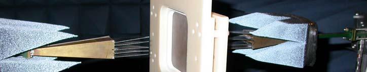
15 Four Pole Tuneable Bandpass Filter Based on SrTiO 3 Discs Duroid SrTiO 3 disk resonator SrTiO 3 disks Diameter: 7.0 mm Thickness: 0.5 mm Plates: Cu/Ti Deleniv et. al. Proc. EuMC 2002
16 Four Pole Tuneable Bandpass Filter Based on SrTiO 3 Discs V 300 V 500 V 0 Transmission coefficient, S21 (db) Reflection coefficient, S21 (db) V 500 V -70 T=77K T=77K 300 V Frequency, GHz Frequency, GHz 3 db bandwidth-2.0%;tuneability-8%; Losses-4.0 db Deleniv et. al. Proc. EuMC 2002
17 Bulk Ceramic Ba x Sr 1-x TiO 3 (Project MELODY)


18 Beam Steering Lens Tageman et. al. Proc. EuMC 2005

19 Tuneable Chip Components: Resonators Capacitors and Delay Lines Pd BST68/32 / MgO 60mol% 6 layers Pd/Ag 1,51 mm 9,22 mm
20 LTCC and HTCC Ba x Sr 1-x TiO 3 (Project MELODY)


21 HTCC Phase Shifters in Project MELODY
22 LTCC OBJECTIVES Development of tunable ferroelectric LTCC compositions Sintering temperature: <950 o C ε= ; tanδ < 0.01 at 2-50 GHz; Tunability >10% Development of processing routes for single and multilayer ferroelectric films with: Thickness 5-50 μm; Area 100x100 mm 2 Development of fabrication routes for electrodes
23 LTCC BSTO Performance 210 Extracted dielectric permittivity, ε r No bias 2V/μm 4V/μm Frequency, GHz tanδ f; (~0.12@25GHz)


24 LTCC Phase Shifters in Project MELODY ~1.5mm TEMEX

25 Measured Phase LTCC Shifter Performance Matching S11, db No bias Frequency, GHz 1.25V/μm 2.4V/μm 4V/μm Phase shift Δφ, deg V/μm Frequency, GHz 4V/μm 2.4V/μm Matching shows weak dependance on DC biasing!!!

 Parallel")
26 Tuneable Power Splitters Coplanar Plate (CPS) Parallel Plate
")

27 Tuneable Matching Networks V1 θ1(v1) Port1 Parallel Plate Port2 Coplanar Plate V2 θ2(v2)
28 Thin film Ba x Sr 1-x TiO 3 (Chalmers) D. Kuylenstierna M. Norling A. Vorobiev A. Deleniv

29 Growth of BST films by laser ablation 0.4 mbar O 2 Laser Rotating Target Ba 0.25 Sr 0.75 TiO x 1 Hz Heater at 650 C PLD System - MC2 Process Lab Chalmers
 50 mtorr Nordiko 2000 Sputter radiation heater")
30 Growth of BST films by rf magnetron sputtering magnet system BSTO 6 target 200W rf Pt/Au/Si substrate Ar ions Ar/O 2 (10/5) 50 mtorr Nordiko 2000 Sputter radiation heater halogen lamps
31 Substrates for ferroelectric microwave Integration devices Issues Crystalline: MgO, LaAlO 3, Al 2 O 3 Polycrystalline: Al 2 O 3 Amorphous: Oxidized Silicon, Fused Silica Metal: Pt, Au, Cu (with diffusion stop buffer)


32 TEM and SEM images of the BSTO films in Thin Film Parallel-Plate Varacotors Top Au/Pt Pt BST BSTO nucleation center Bottom Pt/Au TEM image by Prof. E. Olsson, Chalmers
 Pt (200 nm)-bottom plate Au STO or BSTO Top Plate Au/Pt SiO 2 (0.43 μm) Si substrate 0.")
33 Test Structure Cross Section and Top Electrode Au Au (0.5 μm) -top plate Pt (50 nm) SrTiO 3 (0.56 μm) Pt (200 nm)-bottom plate Au STO or BSTO Top Plate Au/Pt SiO 2 (0.43 μm) Si substrate 0.5 mm Top ground plate, Au/Pt
34 Varactor Performance at 1.0 MHz Capacitance (pf) BST/Pt BST/Pt/Au Q-factor Voltage (V) A. Vorobiev, P. Rundqvist, K. Khamchane, and S. Gevorgian, Appl. Phys. Lett. 83, 3144 (2003)
35 Microwave Performance at V=0 and 20V Capacitance (pf) V 20 V tanδ V 20 V Frequency (GHz) Frequency (GHz) No dispersion in permittivity and tuneability Tuneability > 40 %
36 Technology Comparison. E=0 200 BST/Pt/Au (PLD) GaAs-Schottky Shown are also: Si varactor (Metelics, MSV34,060-C12, 50 MHz, V=-4V) Q-factor BST/Pt (PLD) Si GaAs-HBV 1 10 Frequency (GHz) GaAs HBV (Darmstadt University of Technology, f cut-off =370 GHz) GaAs dual Schottky diode (UMS, DBES105a, f cut-off =2.4 THz)
37 BSTO Potential for Tuneable TFBARs
38 Acoustic Impedances Acoustic impedance Distance from surface Au (63.8) 50 nm Pt (57.6) 300 nm BSTO (42.2) 150 nm Pt (57.6) 0.5 μm Au (63.8) 63.8٠ Si (19.7) 0.45 μm SiO 2
39 Real Part of Impedance (Measured) 0.02 Re(Z)/ V 0 V 20 V Au/Pt/STO/Pt/SiO 2 /Si Frequency, GHz
40 DC Field Dependent Resonance (Measured) V Re{Z}/Im{Z} V Frequency, GHz
41 Device Applications
42 Main Device Fabrication Steps (Prepatterning of bottom electrode) Deposition prepatterning of Pt/Au/Pt (50/500/100nm) bottom electrode Growth of BST film (300nm) by PLD 650 C, 0.4 mbar Top electrode formation by lift-off process


43 Typical Varactor Structures


44 Tuneable Delay Lines Type2
45 Tuneable Delay Line Performance -2.5 S-parameters (0V) E E-11 0V db(s(1,2)) db(s(1,1)) time (s) 7.5E E-11 30V freq, GHz E freq, GHz τ = LC(V ) D. Kuylenstierna et. al, EuMC 2004


46 Lumped Element Tunable Resonators and Filters (a) (b) C S2 /2 C S1 /2 L S2 4L S1 C C L S1 C S2 C C C C C C C S1 L S2 (c) (d)
47 Two-Pole Lumped Element Tunable Filter (simulated) db(s(1,1)) db(s21) freq, GHz freq, GHz D. Kuylenstierna et. al,si RFIC 2006
48 Single Pole Lumped Element Filter (measured) db(s11) db(s21) db(s11) freq, GHz freq, GHz D. Kuylenstierna et. al,si RFIC 2006

49 Tuneable Phase Shifters DC bias 3.6 mm DC bias D. Kuylenstierna et. al, IEEE Micr. Wierless Comp. Letters
50 Tuneable Phase Shifters Mesured S-parameters V 0-5 db(s21) V 0 V db(s11) freq, GHz 15 V Relatively high losses due to steps and surface conductivity of Si D. Kuylenstierna et. al, IEEE Micr. Wierless Comp. Letters
51 Tuneable Phase Shifters Mesured Phase Shift Under 15 V 80 Phase shift [db] Expected phase shift under 25 V: ~90 o freq, GHz D. Kuylenstierna et. al, IEEE Micr. Wierless Comp. Letters
52 Problems and Perspectives
53 Ba x1 Sr 1-x1 TiO 3 Ba x2 Sr 1-x2 TiO 3 Permittivity, ε Paraelectric tanδ Ferroelectric Losses, tanδ Temperature Stabilization (Materials/design based) ε T 2 T 1
54 Temperature Dependence (Materials/Design Based- Measured) Au 2g Au Q Ba 0.75 Sr 0.25 O 3 Ba 0.25 Sr 0.75 O 3 MgO substrate Capacitance, ff Temperature, K C Q-factor
55 Temperature Stabilization (Circuit Topology Based) DC bias network V DC V v L C T V T Varactor C V C
56 Temperature Stabilization (Circuit Topology Based-Summation) E=50 kv/cm Capacitance, pf Not stabilised 0.15 Stabilised Temperature, K
57 Perspective applications : Project HiMission (EUREKA/MEDEA+/VINNOVA ) Phase shifters Tuneable delay Lines Tuneable filters VCO Project Nanostar (FP6, EU) Varactors Tuneable TFBARs VCOs
58 End
Ferroelectrics in agile microwave components
 rmenian Journal of Physics, 2009, vol. 2, issue 1, p. 64-70 Ferroelectrics in agile microwave components Spartak Gevorgian Department of Microtechnology and Nanoscience, Chalmers University of Technology,
MICROWAVE FREQUENCY THIN BST FILM BASED TUNABLE SHUNT AND SERIES INTERDIGITAL CAPACITOR DEVICE DESIGN
 MICROWAVE FREQUENCY THIN BST FILM BASED TUNABLE SHUNT AND SERIES INTERDIGITAL CAPACITOR DEVICE DESIGN Thesis Submitted to The School of Engineering of the UNIVERSITY OF DAYTON In Partial Fulfillment of
SURFACE ACOUSTIC WAVE FERROELECTRIC PHONONIC CRYSTAL TUNABLE BY ELECTRIC FIELD
 NANOSYSTEMS: PHYSICS, CHEMISTRY, MATHEMATICS, 2013, 4 (5), P. 630 634 SURFACE ACOUSTIC WAVE FERROELECTRIC PHONONIC CRYSTAL TUNABLE BY ELECTRIC FIELD V. P. Pashchenko 1,2 1 Saint Petersburg State Polytechnical
Piezoelectric and ferroelectric device technologies for microwave oscillators
 Thesis for the degree of Doctor of Philosophy Piezoelectric and ferroelectric device technologies for microwave oscillators Martin Norling Physical Electronics Laboratory Department of Microtechnology
A Novel Tunable Dual-Band Bandstop Filter (DBBSF) Using BST Capacitors and Tuning Diode
 Using BST Capacitors and Tuning Diode") Progress In Electromagnetics Research C, Vol. 67, 59 69, 2016 A Novel Tunable Dual-Band Bandstop Filter (DBBSF) Using BST Capacitors and Tuning Diode Hassan Aldeeb and Thottam S. Kalkur * Abstract A novel
Progress In Electromagnetics Research C, Vol. 67, 59 69, 2016 A Novel Tunable Dual-Band Bandstop Filter (DBBSF) Using BST Capacitors and Tuning Diode Hassan Aldeeb and Thottam S. Kalkur * Abstract A novel
3D Stacked Buck Converter with SrTiO 3 (STO) Capacitors on Silicon Interposer
 Capacitors on Silicon Interposer") 3D Stacked Buck Converter with SrTiO 3 (STO) Capacitors on Silicon Interposer Makoto Takamiya 1, Koichi Ishida 1, Koichi Takemura 2,3, and Takayasu Sakurai 1 1 University of Tokyo, Japan 2 NEC Corporation,
3D Stacked Buck Converter with SrTiO 3 (STO) Capacitors on Silicon Interposer Makoto Takamiya 1, Koichi Ishida 1, Koichi Takemura 2,3, and Takayasu Sakurai 1 1 University of Tokyo, Japan 2 NEC Corporation,
Hybrid Ferroelectric/Superconducting Microwave Circuits. Robert R. Romanofsky NASA Glenn Research Center Cleveland, OH
 Hybrid Ferroelectric/Superconducting Microwave Circuits Robert R. Romanofsky NASA Glenn Research Center Cleveland, OH Recent progress in processing and deposition techniques along with better modeling
Objective: Competitive Low-Cost Thin-Film Varactor Technology. Integrated Monolithic Capacitors using Sputtered/MOCVD material on low-cost substrates
 Overview of Program Objective: Competitive Low-Cost Thin-Film Varactor Technology coplanar waveguide (CPW) capacitor ground signal ground Si substrate etched troughs Focus of Our Program! Reproducibility!
(Ba, Sr)TiO 3 tunable capacitors with RF commutation quality factors
TiO 3 tunable capacitors with RF commutation quality factors") (Ba, Sr)TiO 3 tunable capacitors with RF commutation quality factors exceeding 6000 Cedric J. G. Meyers 1, Christopher R. Freeze 2, Susanne Stemmer 2, and Robert A. York 1,a) 1 Department of Electrical
(Ba, Sr)TiO 3 tunable capacitors with RF commutation quality factors exceeding 6000 Cedric J. G. Meyers 1, Christopher R. Freeze 2, Susanne Stemmer 2, and Robert A. York 1,a) 1 Department of Electrical
Epitaxial piezoelectric heterostructures for ultrasound micro-transducers
 15 th Korea-U.S. Forum on Nanotechnology Epitaxial piezoelectric heterostructures for ultrasound micro-transducers Seung-Hyub Baek Center for Electronic Materials Korea Institute of Science and Technology
Room-temperature tunable microwave properties of strained SrTiO 3 films
 JOURNAL OF APPLIED PHYSICS VOLUME 96, NUMBER 11 1 DECEMBER 2004 Room-temperature tunable microwave properties of ed SrTiO 3 films Wontae Chang, a) Steven W. Kirchoefer, Jeffrey M. Pond, Jeffrey A. Bellotti,
R. Ludwig and G. Bogdanov RF Circuit Design: Theory and Applications 2 nd edition. Figures for Chapter 6
 R. Ludwig and G. Bogdanov RF Circuit Design: Theory and Applications 2 nd edition Figures for Chapter 6 Free electron Conduction band Hole W g W C Forbidden Band or Bandgap W V Electron energy Hole Valence
Processing and characterization of ferroelectric thin films obtained by pulsed laser deposition
 ELECTROCERAMICS IX, Cherbourg, 2004. Symp. D: Pyro, Piezo, Ferroelectrics: B1-P-578 Processing and characterization of ferroelectric thin films obtained by pulsed laser deposition F. Craciun a,*, M. Dinescu
DIELECTRIC AND TUNABLE BEHAVIOR OF LEAD STRONTIUM TITANATE CERAMICS AND COMPOSITES
 The Pennsylvania State University The Graduate School Intercollege Graduate Program in Materials DIELECTRIC AND TUNABLE BEHAVIOR OF LEAD STRONTIUM TITANATE CERAMICS AND COMPOSITES A Thesis in Materials
Thin Film Bi-based Perovskites for High Energy Density Capacitor Applications
 ..SKELETON.. Thin Film Bi-based Perovskites for High Energy Density Capacitor Applications Colin Shear Advisor: Dr. Brady Gibbons 2010 Table of Contents Chapter 1 Introduction... 1 1.1 Motivation and Objective...
Si, X. X. Xi, and Q. X. JIA
 LA-UR-01-1929 Approved for public release; distribution is unlimited. Title: DIELECTRIC PROPERTIES OF Ba0.6Sr0.4TiO3 THIN FILMS WITH VARIOUS STRAIN STATES Author(s): B. H. PARK, E. J. PETERSON, J. LEE,
Nanoscale Diodes Without p-n Junctions
 Nanoscale Diodes Without p-n Junctions Mircea DRAGOMAN National Institute for Research and Development in Microtechnology (IMT), P.O. Box 38-160, 023573 Bucharest, Romania E-mail: mircea.dragoman@imt.ro
High tunable dielectric response of Pb 0.87 Ba 0.1 La 0.02 (Zr 0.6 Sn 0.33 Ti 0.07 ) O 3 thin film
 O 3 thin film") Journal of Applied Physics, 2010, Volume 108, Issue 4, paper number 044107 High tunable dielectric response of Pb 0.87 Ba 0.1 La 0.02 (Zr 0.6 Sn 0.33 Ti 0.07 ) O 3 thin film T. M. Correia and Q. Zhang*
Journal of Applied Physics, 2010, Volume 108, Issue 4, paper number 044107 High tunable dielectric response of Pb 0.87 Ba 0.1 La 0.02 (Zr 0.6 Sn 0.33 Ti 0.07 ) O 3 thin film T. M. Correia and Q. Zhang*
Investigation of Loss Mechanisms in Thin Film Barium Strontium Titanate Capacitors
 UNIVERSITY OF CALIFORNIA Santa Barbara Investigation of Loss Mechanisms in Thin Film Barium Strontium Titanate Capacitors A Dissertation submitted in partial satisfaction of the requirements for the degree
Size-dependent Metal-insulator Transition Random Materials Crystalline & Amorphous Purely Electronic Switching
 Nanometallic RRAM I-Wei Chen Department of Materials Science and Engineering University of Pennsylvania Philadelphia, PA 19104 Nature Nano, 6, 237 (2011) Adv Mater,, 23, 3847 (2011) Adv Func Mater,, 22,
Design and fabrication of multi-dimensional RF MEMS variable capacitors
 University of South Florida Scholar Commons Graduate Theses and Dissertations Graduate School 2003 Design and fabrication of multi-dimensional RF MEMS variable capacitors Hariharasudhan T. Kannan University
AFRL-SN-WP-TP
 AFRL-SN-WP-TP-25-16 RF PERFORMANCE EVALUATION OF FERROELECTRIC VARACTOR SHUNT SWITCHES Robert Neidhard, Edward Nykiel, John Ebel, Richard Strawser, Keith Stamper, Mark Calcatera, Rand Biggers, Guru Subramanyam
Effect of grain size on the electrical properties of Ba,Ca Zr,Ti O 3 relaxor ferroelectric ceramics
 JOURNAL OF APPLIED PHYSICS 97, 034109 (2005) Effect of grain size on the electrical properties of Ba,Ca Zr,Ti O 3 relaxor ferroelectric ceramics Xin-Gui Tang a) Faculty of Applied Physics, Guangdong University
MME 467: Ceramics for Advanced Applications
 MME 467: Ceramics for Advanced Applications Lecture 26 Dielectric Properties of Ceramic Materials 2 1. Barsoum, Fundamental Ceramics, McGraw-Hill, 2000, pp.513 543 2. Richerson, Modern Ceramic Engineering,
DEPOSITION OF THIN TiO 2 FILMS BY DC MAGNETRON SPUTTERING METHOD
 Chapter 4 DEPOSITION OF THIN TiO 2 FILMS BY DC MAGNETRON SPUTTERING METHOD 4.1 INTRODUCTION Sputter deposition process is another old technique being used in modern semiconductor industries. Sputtering
Fabrication and Characteristic Investigation of Multifunctional Oxide p-n Heterojunctions
 Advances in Science and Technology Vol. 45 (2006) pp. 2582-2587 online at http://www.scientific.net (2006) Trans Tech Publications, Switzerland Fabrication and Characteristic Investigation of Multifunctional
VLSI GATE LEVEL DESIGN UNIT - III P.VIDYA SAGAR ( ASSOCIATE PROFESSOR) Department of Electronics and Communication Engineering, VBIT
 Department of Electronics and Communication Engineering, VBIT") VLSI UNIT - III GATE LEVEL DESIGN P.VIDYA SAGAR ( ASSOCIATE PROFESSOR) contents GATE LEVEL DESIGN : Logic Gates and Other complex gates, Switch logic, Alternate gate circuits, Time Delays, Driving large
VLSI UNIT - III GATE LEVEL DESIGN P.VIDYA SAGAR ( ASSOCIATE PROFESSOR) contents GATE LEVEL DESIGN : Logic Gates and Other complex gates, Switch logic, Alternate gate circuits, Time Delays, Driving large
Applications of Ferroelectrics for Communication Antennas
 Applications of Ferroelectrics for Communication Antennas HRL Research Laboratories Microelectronics Laboratory Jonathan Lynch, jjlynch@hrl.com Joe Colburn, colburn@hrl.com Dave Laney, dclaney@hrl.com
Oxide Films & Nanostructures on Silicon for Thermal Energy Harvesting in Microelectronic Devices
 Oxide Films & Nanostructures on Silicon for Thermal Energy Harvesting in Microelectronic Devices R. Bachelet R. Moalla, A. Carretero-Genevrier, L. Mazet, L. Louahadj, J. Penuelas, B. Vilquin, C. Dubourdieu,
High-Temperature Superconducting Materials for High-Performance RF Filters
 High-Temperature Superconducting Materials for High-Performance RF Filters vakihiko Akasegawa vkazunori Yamanaka vteru Nakanishi vmanabu Kai (Manuscript received February, ) This paper describes the development
Chapter 3 Chapter 4 Chapter 5
 Preamble In recent years bismuth-based, layer-structured perovskites such as SrBi 2 Nb 2 O 9 (SBN) and SrBi 2 Ta 2 O 9 (SBT) have been investigated extensively, because of their potential use in ferroelectric
Dielectric, Piezoelectric and Nonlinear Optical Properties of Lead Titanate based Ferroelectric Thin films
 Dielectric, Piezoelectric and Nonlinear Optical Properties of Lead Titanate based Ferroelectric Thin films Ferroelectric oxides with perovskite structure has gained lot of interest from research as well
Evaluation of kinetic-inductance nonlinearity in a singlecrystal NbTiN-based coplanar waveguide
 Proc. 14th Int. Conf. on Global Research and Education, Inter-Academia 2015 2016 The Japan Society of Applied Physics Evaluation of kinetic-inductance nonlinearity in a singlecrystal NbTiN-based coplanar
Solid State Science and Technology, Vol. 13, No 1 & 2 (2005) ISSN
 ISSN") FABRICATION OF Bi-Ti-O THIN FILM PRESSURE SENSOR PREPARED BY ELECTRON BEAM EVAPORATION METHOD Chong Cheong Wei, Muhammad Yahaya and Muhamad Mat Salleh Institue of Microengineering and Nanoelectronics,
FABRICATION OF Bi-Ti-O THIN FILM PRESSURE SENSOR PREPARED BY ELECTRON BEAM EVAPORATION METHOD Chong Cheong Wei, Muhammad Yahaya and Muhamad Mat Salleh Institue of Microengineering and Nanoelectronics,
LABORATORY of ADVANCED MATERIALS and MICRODEVICES. Prospects and Plans. N. Martirosyan
 LABORATORY of ADVANCED MATERIALS and MICRODEVICES Prospects and Plans N. Martirosyan Topics Categorization of Advanced/Smart Materials High-Temperature Synthesis of Complex Materials Ceramic-Based Devices
Study on the structural and dielectric properties of epitaxial Barium Strontium Titanate (BST) for Tunable Microwave applications.
 for Tunable Microwave applications.") Université du Québec Institut National de la Recherche Scientifique Centre Énergie Matériaux Télécommunications Study on the structural and dielectric properties of epitaxial Barium Strontium Titanate
Université du Québec Institut National de la Recherche Scientifique Centre Énergie Matériaux Télécommunications Study on the structural and dielectric properties of epitaxial Barium Strontium Titanate
CHAPTER 6 DIELECTRIC AND CONDUCTIVITY STUDIES OF ZIRCONIUM TIN TITANATE (ZST)
") 123 CHAPTER 6 DIELECTRIC AND CONDUCTIVITY STUDIES OF ZIRCONIUM TIN TITANATE (ZST) 6.1 INTRODUCTION We know that zirconium tin titanate ceramics are mostly used in microwave frequency applications. Previous
123 CHAPTER 6 DIELECTRIC AND CONDUCTIVITY STUDIES OF ZIRCONIUM TIN TITANATE (ZST) 6.1 INTRODUCTION We know that zirconium tin titanate ceramics are mostly used in microwave frequency applications. Previous
Piezoelectric materials for MEMS applications Hiroshi Funakubo Tokyo Institute of Technology
 Piezoelectric materials for MEMS applications Hiroshi Funakubo Tokyo Institute of Technology MEMS Engineer Forum 2016/5/11 11:50-12:15 Content 1. Introduction 2. Processing 3. Materials Matter Content
1 Name: Student number: DEPARTMENT OF PHYSICS AND PHYSICAL OCEANOGRAPHY MEMORIAL UNIVERSITY OF NEWFOUNDLAND. Fall :00-11:00
 1 Name: DEPARTMENT OF PHYSICS AND PHYSICAL OCEANOGRAPHY MEMORIAL UNIVERSITY OF NEWFOUNDLAND Final Exam Physics 3000 December 11, 2012 Fall 2012 9:00-11:00 INSTRUCTIONS: 1. Answer all seven (7) questions.
Pulsed laser deposition of PZT and PLZT
 Chapter 3 Pulsed laser deposition of PZT and PLZT A lower growth temperature of PZT films is favored for integration of these films for MEMS application. This chapter gives a detailed account of the work
Reducing AC impedance measurement errors caused by the DC voltage dependence of broadband high-voltage bias-tees
 27 IEEE International Conference on Microelectronic Test Structures, March 19-22, Tokyo, Japan. 8.11 Reducing AC impedance measurement errors caused by the DC voltage dependence of broadband high-voltage
Dielectric Properties of Composite Films Made from Tin(IV) Oxide and Magnesium Oxide
 Oxide and Magnesium Oxide") OUSL Journal (2014) Vol 7, (pp67-75) Dielectric Properties of Composite Films Made from Tin(IV) Oxide and Magnesium Oxide C. N. Nupearachchi* and V. P. S. Perera Department of Physics, The Open University
OUSL Journal (2014) Vol 7, (pp67-75) Dielectric Properties of Composite Films Made from Tin(IV) Oxide and Magnesium Oxide C. N. Nupearachchi* and V. P. S. Perera Department of Physics, The Open University
Diamond-like carbon film deposition on PZT ferroelectrics and YBCO superconducting films using KrF excimer laser deposition
 Composites: Part B 30 (1999) 685 689 www.elsevier.com/locate/compositesb Diamond-like carbon film deposition on PZT ferroelectrics and YBCO superconducting films using KrF excimer laser deposition K. Ebihara*,
Barium Strontium Titanate films for tunable microwave and acoustic wave applications
 University of South Florida Scholar Commons Graduate Theses and Dissertations Graduate School 2007 Barium Strontium Titanate films for tunable microwave and acoustic wave applications Venkataramanan Gurumurthy
Lecture 040 Integrated Circuit Technology - II (5/11/03) Page ECE Frequency Synthesizers P.E. Allen
 Page ECE Frequency Synthesizers P.E. Allen") Lecture 040 Integrated Circuit Technology - II (5/11/03) Page 040-1 LECTURE 040 INTEGRATED CIRCUIT TECHNOLOGY - II (Reference [7,8]) Objective The objective of this presentation is: 1.) Illustrate and
Lecture 040 Integrated Circuit Technology - II (5/11/03) Page 040-1 LECTURE 040 INTEGRATED CIRCUIT TECHNOLOGY - II (Reference [7,8]) Objective The objective of this presentation is: 1.) Illustrate and
Leakage Mechanisms. Thin films, fully depleted. Thicker films of interest for higher voltage applications. NC State
 Leakage Mechanisms Thin films, fully depleted Leakage controlled by combined thermionic / field emission across the Schottky barrier at the film-electrode interfaces. Film quality effects barrier height,
Effect of Spiral Microwave Antenna Configuration on the Production of Nano-crystalline Film by Chemical Sputtering in ECR Plasma
 THE HARRIS SCIENCE REVIEW OF DOSHISHA UNIVERSITY, VOL. 56, No. 1 April 2015 Effect of Spiral Microwave Antenna Configuration on the Production of Nano-crystalline Film by Chemical Sputtering in ECR Plasma
RECONFIGURABLE PASSIVE RF/MICROWAVE COMPONENTS. Dissertation. Submitted to. The School of Engineering of the UNIVERSITY OF DAYTON
 RECONFIGURABLE PASSIVE RF/MICROWAVE COMPONENTS Dissertation Submitted to The School of Engineering of the UNIVERSITY OF DAYTON In Partial Fulfillment of the Requirements for The Degree of Doctor of Philosophy
Defense Technical Information Center Compilation Part Notice
 UNCLASSIFIED Defense Technical Information Center Compilation Part Notice ADP013368 TITLE: Microwave Phase Shifters Using Ferroelectric [Ba,Sr]TiO3 Films DISTRIBUTION: Approved for public release, distribution
Supplementary Figure 1: SAW transducer equivalent circuit
 Supplementary Figure : SAW transducer equivalent circuit Supplementary Figure : Radiation conductance and susceptance of.6um IDT, experiment & calculation Supplementary Figure 3: Calculated z-displacement
Introduction to CMOS RF Integrated Circuits Design
 V. Voltage Controlled Oscillators Fall 2012, Prof. JianJun Zhou V-1 Outline Phase Noise and Spurs Ring VCO LC VCO Frequency Tuning (Varactor, SCA) Phase Noise Estimation Quadrature Phase Generator Fall
Infrastructure of Thin Films Laboratory in Institute of Molecular Physics Polish Academy of Sciences
 Infrastructure of Thin Films Laboratory in Institute of Molecular Physics Polish Academy of Sciences Outline Sample preparation Magnetron sputtering Ion-beam sputtering Pulsed laser deposition Electron-beam
MICROWAVE SURFACE IMPEDANCE OF A NEARLY FERROELECTRIC SUPERCONDUCTOR
 Progress In Electromagnetics Research, PIER 73, 39 47, 2007 MICROWAVE SURFACE IMPEDANCE OF A NEARLY FERROELECTRIC SUPERCONDUCTOR C.-J. Wu Department of Applied Physics National University of Kaohsiung
Thermoelectric Oxide Materials For Electric Power Generation
 Thermoelectric Oxide Materials For Electric Power Generation Kunihito Koumoto Nagoya University, Graduate School of Engineering CREST, Japan Science and Technology Agency 1. Thermoelectric Energy Conversion
Relaxor characteristics of ferroelectric BaZr 0.2 Ti 0.8 O 3 ceramics
 Materials Science-Poland, Vol. 27, No. 3, 2009 Relaxor characteristics of ferroelectric BaZr 0.2 Ti 0.8 O 3 ceramics C. FU 1, 2*, F. PAN 1, W. CAI 1, 2, X. DENG 2, X. LIU 2 1 School of Materials Science
Lecture 23: Negative Resistance Osc, Differential Osc, and VCOs
 EECS 142 Lecture 23: Negative Resistance Osc, Differential Osc, and VCOs Prof. Ali M. Niknejad University of California, Berkeley Copyright c 2005 by Ali M. Niknejad A. M. Niknejad University of California,
Design and Modeling of Membrane Supported FBAR Filter
 Design and Modeling of Membrane Supported FBAR Filter Alexandra STEFANESCU, Dan NECULOIU, Alina Cristina BUNEA IMT Bucharest, 32B, Erou Iancu Nicolae str., 077190 Bucharest, Romania Tel.: +40212690775
Low-loss superconducting resonant circuits using vacuum-gap-based microwave components
 Low-loss superconducting resonant circuits using vacuum-gap-based microwave components Katarina Cicak 1, Dale Li 1, Joshua A. Strong 1,2, Michael S. Allman 1,2, Fabio Altomare 1, Adam J. Sirois 1,2, Jed
Plasma Deposition (Overview) Lecture 1
 Lecture 1") Plasma Deposition (Overview) Lecture 1 Material Processes Plasma Processing Plasma-assisted Deposition Implantation Surface Modification Development of Plasma-based processing Microelectronics needs (fabrication
Plasma Deposition (Overview) Lecture 1 Material Processes Plasma Processing Plasma-assisted Deposition Implantation Surface Modification Development of Plasma-based processing Microelectronics needs (fabrication
Physical and Dielectric Properties of Silver Lithium Niobate Mixed Ceramic System
 American Journal of Materials Science and Engineering, 213, Vol. 1, No. 3, 54-59 Available online at http://pubs.sciepub.com/ajmse/1/3/5 Science and Education Publishing DOI:1.12691/ajmse-1-3-5 Physical
Accurate Modeling of Spiral Inductors on Silicon From Within Cadence Virtuoso using Planar EM Simulation. Agilent EEsof RFIC Seminar Spring 2004
 Accurate Modeling of Spiral Inductors on Silicon From Within Cadence Virtuoso using Planar EM Simulation Agilent EEsof RFIC Seminar Spring Overview Spiral Inductor Models Availability & Limitations Momentum
Characteristic of Capacitors
 3.5. The Effect of Non ideal Capacitors Characteristic of Capacitors 12 0 (db) 10 20 30 capacitor 0.001µF (1000pF) Chip monolithic 40 two-terminal ceramic capacitor 0.001µF (1000pF) 2.0 x 1.25 x 0.6 mm
Supplementary Figure S1. AFM images of GraNRs grown with standard growth process. Each of these pictures show GraNRs prepared independently,
 Supplementary Figure S1. AFM images of GraNRs grown with standard growth process. Each of these pictures show GraNRs prepared independently, suggesting that the results is reproducible. Supplementary Figure
J. Price, 1,2 Y. Q. An, 1 M. C. Downer 1 1 The university of Texas at Austin, Department of Physics, Austin, TX
 Understanding process-dependent oxygen vacancies in thin HfO 2 /SiO 2 stacked-films on Si (100) via competing electron-hole injection dynamic contributions to second harmonic generation. J. Price, 1,2
Microstructures and Dielectric Properties of Ba 1 x Sr x TiO 3 Ceramics Doped with B 2 O 3 -Li 2 O Glasses for LTCC Technology Applications
 J. Mater. Sci. Technol., 212, 28(3), 28 284. Microstructures and Dielectric Properties of Ba 1 x Sr x TiO 3 Ceramics Doped with B 2 O 3 -Li 2 O Glasses for LTCC Technology Applications Xiujian Chou 1),
UNIVERSITY OF CALIFORNIA College of Engineering Department of Electrical Engineering and Computer Sciences. Professor Chenming Hu.
 UNIVERSITY OF CALIFORNIA College of Engineering Department of Electrical Engineering and Computer Sciences EECS 130 Spring 2009 Professor Chenming Hu Midterm I Name: Closed book. One sheet of notes is
Recent Developments in Magnetoelectrics Vaijayanti Palkar
 Recent Developments in Magnetoelectrics Vaijayanti Palkar Department of Condensed Matter Physics & Materials Science Tata Institute of Fundamental Research Mumbai 400 005, India. Tata Institute of Fundamental
Lecture 18. New gas detectors Solid state trackers
 Lecture 18 New gas detectors Solid state trackers Time projection Chamber Full 3-D track reconstruction x-y from wires and segmented cathode of MWPC z from drift time de/dx information (extra) Drift over
Microstrip Coupler with Complementary Split-Ring Resonator (CSRR)
") Microstrip Coupler with Complementary Split-Ring Resonator (CSRR) E-242 Course Project Report Submitted by, EMIL MATHEW JOSEPH 4810-411-091-07049 Guided by, Prof. K J VINOY Department of Electrical and
Microstrip Coupler with Complementary Split-Ring Resonator (CSRR) E-242 Course Project Report Submitted by, EMIL MATHEW JOSEPH 4810-411-091-07049 Guided by, Prof. K J VINOY Department of Electrical and
ELEN0037 Microelectronic IC Design. Prof. Dr. Michael Kraft
 ELEN0037 Microelectronic IC Design Prof. Dr. Michael Kraft Lecture 2: Technological Aspects Technology Passive components Active components CMOS Process Basic Layout Scaling CMOS Technology Integrated
GHZ ELECTRICAL PROPERTIES OF CARBON NANOTUBES ON SILICON DIOXIDE MICRO BRIDGES
 GHZ ELECTRICAL PROPERTIES OF CARBON NANOTUBES ON SILICON DIOXIDE MICRO BRIDGES SHENG F. YEN 1, HAROON LAIS 1, ZHEN YU 1, SHENGDONG LI 1, WILLIAM C. TANG 1,2, AND PETER J. BURKE 1,2 1 Electrical Engineering
INVESTIGATION OF TEMPERATURE DEPENDENCES OF ELECTROMECHANICAL PROPERTIES OF PLZT CERAMICS
 Molecular and Quantum Acoustics vol. 28 (2007) 47 INVESTIGATION OF TEMPERATURE DEPENDENCES OF ELECTROMECHANICAL PROPERTIES OF PLZT CERAMICS M. CZERWIEC, R. ZACHARIASZ and J. ILCZUK Department of Material
Electronic Supplementary Information: Synthesis and Characterization of Photoelectrochemical and Photovoltaic Cu2BaSnS4 Thin Films and Solar Cells
 Electronic Supplementary Material (ESI) for Journal of Materials Chemistry C. This journal is The Royal Society of Chemistry 2017 Electronic Supplementary Information: Synthesis and Characterization of
Paper V. Acoustic Radiation Losses in Busbars. J. Meltaus, S. S. Hong, and V. P. Plessky J. Meltaus, S. S. Hong, V. P. Plessky.
 Paper V Acoustic Radiation Losses in Busbars J. Meltaus, S. S. Hong, and V. P. Plessky 2006 J. Meltaus, S. S. Hong, V. P. Plessky. V Report TKK-F-A848 Submitted to IEEE Transactions on Ultrasonics, Ferroelectrics,
Tunable MEMS Capacitor for RF Applications
 Tunable MEMS Capacitor for RF Applications Shriram H S *1, Tushar Nimje 1, Dhruv Vakharia 1 1 BITS Pilani, Rajasthan, India *1167, 1 st Main, 2 nd Block, BEL Layout, Vidyaranyapura, Bangalore 560097; email:
Ba x Sr 1-x TiO 3 /pc-si HETEROJUNCTION
 Armenian Journal of Physics, 2013, vol. 6, issue 4, pp. 177-187 Ba x Sr 1-x TiO 3 /pc-si HTROJUNCTION V. BUNIATYAN 1, C. HUCK 2, A. POGHOSSIAN 2, V.M. AROUTIOUNIAN 3, and M.J. SCHONING 2 1 State ngineering
SUPPLEMENTARY INFORMATION
 doi:10.1038/nature11231 Materials and Methods: Sample fabrication: Highly oriented VO 2 thin films on Al 2 O 3 (0001) substrates were deposited by reactive sputtering from a vanadium target through reactive
Piezoelectric Resonators ME 2082
 Piezoelectric Resonators ME 2082 Introduction K T : relative dielectric constant of the material ε o : relative permittivity of free space (8.854*10-12 F/m) h: distance between electrodes (m - material
Energy storage: high performance material engineering
 Energy storage: high performance material engineering Teranishi Group Faculty of Engineering Research activities 1) Polarization assisted ultrahigh rate lithium ion batteries 1) Lithium ion conductor-dielectrics
ABSTRACT 1. INTRODUCTION 2. EXPERIMENT
 Fabrication of Nanostructured Heterojunction LEDs Using Self-Forming Moth-Eye Type Arrays of n-zno Nanocones Grown on p-si (111) Substrates by Pulsed Laser Deposition D. J. Rogers 1, V. E. Sandana 1,2,3,
A new method of dielectric characterization in the microwave range for high-k ferroelectric thin films
 A new method of dielectric characterization in the microwave range for high-k ferroelectric thin films Kevin Nadaud, Hartmut Gundel, Caroline Borderon, Raphaël Gillard, Erwan Fourn To cite this version:
The Basic Capacitor. Dielectric. Conductors
 Chapter 9 The Basic Capacitor Capacitors are one of the fundamental passive components. In its most basic form, it is composed of two conductive plates separated by an insulating dielectric. The ability
Photocarrier Injection and Current Voltage Characteristics of La 0:8 Sr 0:2 MnO 3 /SrTiO 3 :Nb Heterojunction at Low Temperature
 Japanese Journal of Applied Physics Vol. 44, No. 1, 25, pp. 7367 7371 #25 The Japan Society of Applied Physics Photocarrier Injection and Current Voltage Characteristics of La :8 Sr :2 MnO 3 /SrTiO 3 :Nb
* Received 18 November 2013
 Armenian Journal of Physics, 2013, vol. 6, issue 4, pp. 188-197 Ba x Sr 1-x TiO 3 /pc-si HTROJUNCTION CAPACITANC V. BUNIATYAN 1*, C.HUCK 2, A. POGHOSSIAN 2, V. M. AROUTIOUNIAN 3, and M.J. SCHONING 2 1
Zero-biased YBCO detectors for the real-time observation of coherent synchrotron radiation
 Zero-biased YBCO detectors for the real-time observation of KSETA Plenary Workshop, 13-15 February 217, Durbach J. Raasch Institut für Mikro- und Nanoelektronische Systeme (IMS) KIT University of the State
ECE 340 Lecture 39 : MOS Capacitor II
 ECE 340 Lecture 39 : MOS Capacitor II Class Outline: Effects of Real Surfaces Threshold Voltage MOS Capacitance-Voltage Analysis Things you should know when you leave Key Questions What are the effects
Ultrafast Optoelectronic Study of Superconducting Transmission Lines
 Ultrafast Optoelectronic Study of Superconducting Transmission Lines Shinho Cho, Chang-Sik Son and Jonghun Lyou Presented at the 8th International Conference on Electronic Materials (IUMRS-ICEM 2002, Xi
GaN based transistors
 GaN based transistors S FP FP dielectric G SiO 2 Al x Ga 1-x N barrier i-gan Buffer i-sic D Transistors "The Transistor was probably the most important invention of the 20th Century The American Institute
PAD MODELING BY USING ARTIFICIAL NEURAL NETWORK
 Progress In Electromagnetics Research, PIER 74, 167 180, 2007 PAD MODELING BY USING ARTIFICIAL NEURAL NETWORK X. P. Li School of Telecommunication Engineering Beijing University of Posts and Telecommunications
CIRCUIT ELEMENT: CAPACITOR
 CIRCUIT ELEMENT: CAPACITOR PROF. SIRIPONG POTISUK ELEC 308 Types of Circuit Elements Two broad types of circuit elements Ati Active elements -capable of generating electric energy from nonelectric energy
Supporting Online Material for
 www.sciencemag.org/cgi/content/full/327/5966/662/dc Supporting Online Material for 00-GHz Transistors from Wafer-Scale Epitaxial Graphene Y.-M. Lin,* C. Dimitrakopoulos, K. A. Jenkins, D. B. Farmer, H.-Y.
ECE 497 JS Lecture -07 Planar Transmission Lines
 ECE 497 JS Lecture -07 Planar Transmission Lines Spring 2004 Jose E. Schutt-Aine Electrical & Computer Engineering University of Illinois jose@emlab.uiuc.edu 1 Microstrip ε Z o w/h < 3.3 2 119.9 h h =
Structural and electro-optic properties of Ba 0.7 Sr 0.3 TiO 3 thin films grown on various substrates using pulsed laser deposition
 JOURNAL OF APPLIED PHYSICS 101, 043515 2007 Structural and electro-optic properties of Ba 0.7 Sr 0.3 TiO 3 thin films grown on various substrates using pulsed laser deposition D. Y. Wang, a J. Wang, H.
arxiv: v1 [cond-mat.mtrl-sci] 9 Apr 2007
![arxiv: v1 [cond-mat.mtrl-sci] 9 Apr 2007](/thumbs/93/118034102.jpg "arxiv: v1 [cond-mat.mtrl-sci] 9 Apr 2007") Electrical transport properties of polar heterointerface between KTaO 3 and SrTiO 3 A. Kalabukhov, 1, R. Gunnarsson, 1 T. Claeson, 1 and D. Winkler 1 arxiv:0704.1050v1 [cond-mat.mtrl-sci] 9 Apr 2007 1
Electrical transport properties of polar heterointerface between KTaO 3 and SrTiO 3 A. Kalabukhov, 1, R. Gunnarsson, 1 T. Claeson, 1 and D. Winkler 1 arxiv:0704.1050v1 [cond-mat.mtrl-sci] 9 Apr 2007 1
ECE 451 Transmission Lines & Packaging
 Transmission Lines & Packaging Jose E. Schutt-Aine Electrical & Computer Engineering University of Illinois jose@emlab.uiuc.edu 1 Radio Spectrum Bands The use of letters to designate bands has long ago
SUPPLEMENTARY MATERIALS FOR PHONON TRANSMISSION COEFFICIENTS AT SOLID INTERFACES
 148 A p p e n d i x D SUPPLEMENTARY MATERIALS FOR PHONON TRANSMISSION COEFFICIENTS AT SOLID INTERFACES D.1 Overview The supplementary information contains additional information on our computational approach
Multilayer Ceramic Capacitors Leaded Capacitors. Packaging. Internal coding. Capacitance tolerance
 Leaded Capacitors Leaded Ordering code system B37979N 1 100 K 0 54 Packaging 51 ^ cardboard tape, reel packing (360-mm reel) 54 ^ Ammo packing (standard) 00 ^ bulk Internal coding Capacitance tolerance
Omar M. Ramahi University of Waterloo Waterloo, Ontario, Canada
 Omar M. Ramahi University of Waterloo Waterloo, Ontario, Canada Traditional Material!! Electromagnetic Wave ε, μ r r The only properties an electromagnetic wave sees: 1. Electric permittivity, ε 2. Magnetic
Electrical Characterization with SPM Application Modules
 Electrical Characterization with SPM Application Modules Metrology, Characterization, Failure Analysis: Data Storage Magnetoresistive (MR) read-write heads Semiconductor Transistors Interconnect Ferroelectric
Capacitors. Charging a Capacitor. Charge and Capacitance. L05: Capacitors and Inductors
 L05: Capacitors and Inductors 50 Capacitors 51 Outline of the lecture: Capacitors and capacitance. Energy storage. Capacitance formula. Types of capacitors. Inductors and inductance. Inductance formula.