A Nanoscale PN Junction in Series with Tunable. Schottky Barriers
|
|
|
- Zoe Randall
- 5 years ago
- Views:
Transcription
1 1 A Nanoscale PN Junction in Series with Tunable Schottky Barriers Lee Aspitarte, Daniel R. McCulley, Ethan D. Minot* Department of Physics, Oregon State University, Corvallis, OR, 97331, USA * Corresponding author ethan.minot@oregonstate.edu Abstract PN junctions in nanoscale materials are of interest for a range of technologies including photodetectors, solar cells and light-emitting diodes. However, Schottky barriers at the interface between metal contacts and the nanomaterial are often unavoidable. The effect of metalsemiconductor interfaces on the behavior of nanoscale diodes must be understood, both to extract the characteristics of the pn junction, and to understand the overall characteristics of the final device. Here, we study the current-voltage characteristics of diodes that are formed in fullysuspended carbon nanotubes. We utilize tunable Schottky barrier heights at the CNT-metal interface to elucidate the role of the Schottky barriers on the device characteristics. We develop a quantitative model to show how a variety of device characteristics can arise from apparently similar devices. Using our model we extract key parameters of the Schottky barriers and the pn junction, and predict the overall I-V characteristics of the device. Our equivalent circuit model is relevant to a variety of nanomaterial-based diode devices that are currently under investigation.
2 2 INTRODUCTION The pn junction is a crucial building block for modern electronics and optoelectronics. Researchers have recently created and studied pn junctions in a variety of nanoscale semiconducting materials, including carbon nanotubes (CNTs) 1 and transition metal dichalcogenides (reviewed in [2]). These nanomaterial-based pn junctions are being investigated for their potential applications as rectifying diodes, solar cells, photodetectors and LEDs. Measurements of pn junctions in nanomaterials are often complicated by metal-semiconductor contacts. Previous work has shown that Schottky barriers associated with metal-semiconductor contacts drastically affect the electrical characteristics of nanomaterial-based field-effect transistors. 3 5 However, the effect of Schottky barriers on the electrical characteristics of nanomaterial-based diodes is relatively unexplored. For example, CNT diode devices have been reported with a diversity of electrical characteristics that cannot be accounted for by a simple pn junction. 6,7 In this work, we elucidate the role of Schottky barriers in lateral pn-junction devices made from individual suspended carbon nanotubes. We vary the Schottky barrier heights (SBHs) and establish the effect of Schottky contacts on the overall properties the nanoscale diode. We have chosen suspended CNTs with dual gates as our model system (Fig. 1a). Dual-gated CNTs have received considerable attention in recent years, due to their promising electronic and optoelectronic characteristics Fully-suspended dual-gated CNTs are an ideal model system for exploring the role of Schottky contacts on nanoscale diodes. First, the fully-suspended CNT is a clean system. There are no complications associated with substrate-induced disorder, doping, or screening. 17 Second, we can characterize the diameter and chirality of the CNT under study, 15 allowing precise comparison between device characteristics and electronic structure. Third, our device geometry creates Schottky barriers that are sufficiently long (> 100 nm) so that
3 3 transport past the barrier is via thermionic emission, rather than a complicated mixture of tunneling and thermionic emission. 3,4 Lastly, the SBH is tunable. The work function (WF) of the metal contacts changes gradually when the device is transferred from laboratory air to a vacuum environment. Previous authors have used this affect to study the role of SBH on CNT field-effect transistors (CNT FETs), 18,19 and here we use the effect for the first time to study the role of SBH on a nanomaterial-based diode. METHODS Ultra-clean suspended CNTs were fabricated by growing CNTs over pre-made electrode structures. Electrodes were fabricated on 4-inch Si/SiO2 wafers (500 nm oxide layer). First, the pair of gate electrodes were patterned and deposited (W/Pt 5 nm/60 nm). The separation distance between gate electrodes is 200 nm. The gate electrodes were then buried by SiO2 (800 nm thickness) and source/drain electrode pairs were patterned and deposited (W/Pt 5 nm/60 nm). The separation distance between source and drain electrodes is 2 m. Reactive-ion etching was used to make a 700-nm-deep trench between the source and drain electrodes. The source and drain electrodes serve as an etch mask to define the edge of the trench. CNT growth catalyst (1 nm Ti / 20 nm SiO2 / 1 nm Fe) was patterned and deposited on top of the source and drain electrodes. CNTs were grown using chemical vapor deposition in a tube furnace at 800 C. The chips were shuttled in/out of the furnace hot zone to minimize heat exposure. The growth recipe consists of a 1 minute 1 SLM H2 anneal followed by a 5 minute growth phase with 0.15 SLM ethanol, 0.3 SLM methanol, and 0.45 SLM H2. The ethanol and methanol are introduced into Ar gas with a bubbler.
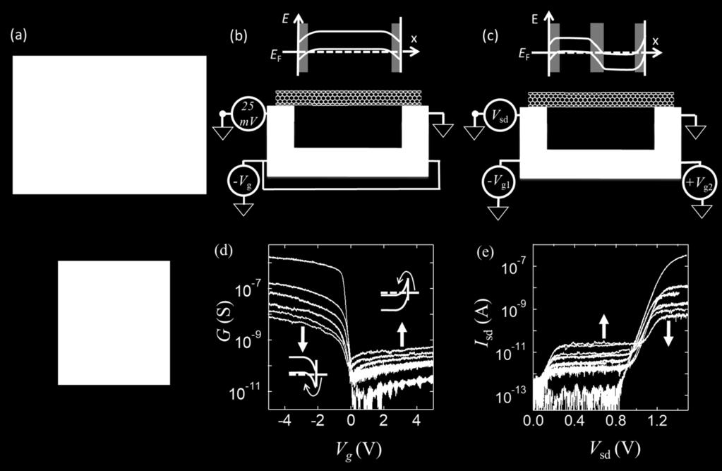
4 4 After device fabrication, electrode pairs that are connected by individual CNTs were identified by electrical characterization and scanning photocurrent microscopy. Spectrally-resolved photocurrent was used to determine the diameter and chirality of the CNT under study. 15 RESULTS AND DISCUSSION We first verify the role of the SBH on the transport characteristics of a suspended CNT FET. Figure 1d shows the measured G(Vg) of a dual-gated suspended CNT. The CNT chiral index is (29, 10) which corresponds to a diameter of 2.74 nm and an S11 optical resonance energy of 430 mev (see Figure S2). To perform field-effect transistor measurements, the gates are configured such that Vg1 = Vg2. A variety of SBHs were achieved by transferring the device from laboratory air to vacuum. Measurements were performed in vacuum over the course of 2 weeks. Consistent with the previous literature, the p-type conductivity of the CNT FET decreases as a function of time spent in vacuum, while the n-type conductivity increases (Figure 1d). 15 The n-type and p- type conductivities are related to the electron SBH, Φ, and the hole SBH, Φ, respectively (Figure 1d, inset). As previously explained by McClain et al., 18 a reduction in metal WF over time leads to a decrease in Φ and increase in Φ, consistent with our transport measurements. In a material with a homogeneous transport band gap, Eg, we expect Φ Φ to equal the bandgap, therefore a decrease in Φ will be balanced by an increase in Φ.
 Cross-sectional diagram and band diagram for the device when operated as a CNT FET. c) Device schematic and band diagram for the device when operated as a diode.")
5 5 Figure 1: Comparison of the CNT FET characteristics and the CNT diode characteristics. a) Schematic diagram of the device geometry. All dimensions are to scale except for the CNT. b) Cross-sectional diagram and band diagram for the device when operated as a CNT FET. c) Device schematic and band diagram for the device when operated as a diode. d) Conductance of the CNT FET measured with Vsd = 25 mv. The black curve is measured in laboratory air. The color of the curves changes from dark green to orange as the device is left in vacuum for two weeks. All measurements are taken at T = 295 K. e) CNT diode characteristics measured at Vg1 = -Vg2 = -5 V over the same time period. The diode characteristics of the same CNT device were measured as the metal WF was varied (Fig. 1e). After each field-effect transistor measurement, the gates were reconfigured such that Vg1 = -Vg2 = -5 V. Figure 1e shows the resulting Isd-Vsd characteristics for Vsd > 0. In reverse bias (not shown) the current is below the noise floor of our current amplifier ( I < A, see Fig. S1a). In ambient environment (black curve), the forward-biased current remains below the noise floor of our measurement for Vsd < 0.8 V. For Vsd > 0.8 V, The current increases exponentially before finally rolling off into a linear Isd-Vsd relationship. After one day in vacuum (dark green curve), the device characteristics dramatically change. Unlike a conventional diode, we observe
6 6 two regimes where the current exponentially increases and two regimes where the current plateaus. The first exponential increase begins near V sd = 0 V. The voltage threshold for the second exponential increase is variable, changing with the number of days in vacuum (Fig. 1e), and with the magnitude of the applied gate voltages (see supplementary information, Figure S1b). As the device sits in vacuum over the course of two weeks, the current level of the first plateau increases, while the current level of the second plateau decreases. We have developed an equivalent circuit model that explains the observed diode characteristics. As shown in Figure 2a, the pn junction in the center of the CNT is in series with two reverse-biased Schottky diodes. One Schottky diode is associated with the junction between the source electrode and the p-doped section of CNT. The other Schottky diode is associated with the junction between the drain electrode and the n-doped section of CNT. We assume that majority charge carriers thermalize in the sections of CNT connecting the three circuit elements. In our model, the current plateaus correspond to the saturation currents of the Schottky diodes (Fig. 2d, regions labeled R2 and R4). The pn junction determines the current before the first plateau and in-between the plateaus (Fig. 2d, regions labeled R1 and R3). We now formalize this model and quantify the key parameters for the device shown in Fig. 1e.
7 7 Figure 2. a) Equivalent circuit for the suspended CNT pn junction. b,c) Schematic band diagrams along the axis of the CNT for the regimes R2 and R4 as labeled in part d. d) Simulated Isd-Vsd characteristic that closely match Fig. 1e. The SBH heights are varied from e = 250 mev (dark green) to e = 170 mev (orange), maintaining e + h = 410 mev. Other free parameters are fixed: h = 1, e = , pn = 1, n = 1.3, Eg = 500 mev and Vshift = 0.9 V. that The source-drain bias, Vsd, is distributed across the three circuit elements shown in Fig. 2a such V sd = V SBh + V pn + V SBe, (1) The current through each circuit element must be equal, yielding the condition I sd = I SBh = I pn = I SBe. Thus, Isd is constrained by the coupled equations: I SBh = I 0,SBh 1 e ev SBh k BT (2) evpn I pn = I 0,pn nk BT 1 (3) I SBe = I 0,SBe 1 ev SBe k BT, V SBe < V shift (4a,b) G 0 V SBe - V shift, V SBe > V shift
8 8 where I0,SBh, I0,pn, and I0,SBe are the saturation currents of the respective diodes, n is the ideality factor of the pn junction, G0 is the conductance quantum, and Vshift is a critical voltage at which the transport mechanism changes for ISBe. Equations 2 and 4a are flipped in sign compared to a conventional Schottky diode due to the reversed orientation. The piecewise function (eq. 4) describes an unusual voltage dependence of ISBe. A mechanism for this voltage-triggered change was proposed by Liu et al. 7 The length of the n-doped region, Ln, becomes smaller as VSBe is increased. When Ln is sufficiently short (V SBe > V shift, holes are transmitted directly from the p-doped region to the drain electrode without recombination (Fig 2c). In this regime, the hole current bypasses the Schottky barrier for electrons. To complete our model, we consider the factors influencing the saturation currents I0,SBh, I0,pn, and I0,SBe. Using a 1-D Landauer formalism for electron transport in a CNT, Bosnik et al. calcuated 20 I 0,pn τ e Eg k BT, (5) where τ is the transmission coefficient over the pn junction and Eg is the bandgap of the CNT at the location of the pn junction (Eg >> kbt). Applying the same approach to a 1-D Schottky contact yields I 0,SBh I 0,SBe e Φ k B T (6) e Φ k BT, (7) where h and e are the Schottky barrier heights for holes and electrons, and and are the transmission coefficients across the two Schottky barriers. Equations (6) and (7) are consistent with the 1D Richardson constant formalism previously used to analyze CNT 1D contacts. 4,21
9 9 Figure 2d shows solutions to the coupled set of equations, Eqs These curves were generated by determining the voltage drop across each circuit element for a given Isd, (see supplementary note 1). The free parameters h, e, pn, n, Eg and Vshift are the same for all 5 curves and we constrain h + e = 410 mev, as discussed further below. The simulated device characteristics (Fig. 2d) are in excellent agreement with our measurements (Fig. 1e). It is instructive to qualitatively describe the features of Fig. 2d. The four distinct regimes of Isd(Vsd) are labeled in Fig. 2d as R1, R2, R3 and R4. In R1, the current-limiting circuit element is the pn junction. This can be understood by calculating the zero-bias conductance of each circuit element. We expect the pn junction to have the smallest zero bias conductance because Eg is greater than either h or e, therefore I 0,pn is much less than I 0,SBh or I 0,SBe. In R2, the currentlimiting circuit element is the reverse-biased Schottky barrier for electrons and the current plateau occurs at I 0,SBe. In R3, the Schottky barrier for electrons is by-passed, and the currentlimiting circuit element is the pn junction. Finally, in R4, the current-limiting circuit element is the reverse-biased Schottky barrier for holes and the current plateau occurs at I 0,SBh. Temperature-dependent measurements are useful for testing our model and for constraining the model parameters. Figure 3a shows measurements of the diode characteristics on Day 15 (Vg1 = - Vg2 = -5 V) as the temperature, T, is varied from 300 K to 200 K in steps of 25 K. The current at the plateaus is exponentially suppressed as T is lowered. From our equivalent circuit model we associate the first plateau with I 0,SBe and the second plateau with I 0,SBh. As shown in Fig. 3b, the exponential suppression of I 0,SBe and I 0,SBh agrees with the predictions of Eqn. 6 and Eqn. 7. Using Eqn. 6 and 7 to fit the temperature dependence of the current plateaus we find Φ e = 192 ± 14 mev, Φ h = 219 ± 24 mev and < e < and 0.4 < h < 3.9.
10 10 Figure 3: Extracting the SBH height from temperature dependent Isd-Vsd characteristics. a) Temperature dependent diode curves (same device as Fig. 1e). b) 1D Richardson plot of the first (red) and second (blue) current plateaus. Solid lines are fits to Eqn. 6 and 7. The extracted Schottky barrier heights are Φ e = 192 ± 14 mev and Φ h = 219 ± 24 mev. Our electrical measurements give a quantitative estimate of Φ Φ h 410 mev, which we now compare to the CNT chiral index. The chiral index of this CNT is (n, m) = (29, 10) which has a lowest-energy exciton resonance S11 = 430 mev (see Figure S2). Within experimental uncertainty, S11 is equal to our electronic measurement Φ Φ h = 410 ± 30 mev. The equality between S11 and Φ Φ h suggests that electron-electron interactions are strongly screened at the location where the Schottky barriers form. This is a reasonable assumption, because the Schottky barriers are in close proximity to the metal electrodes.
11 11 In contrast to the electrostatically-screened environment near the metal electrodes, the pn junction is located in the center of the CNT, far from the metal electrodes. Previous experiments on CNT pn junctions, 22 scanning tunneling spectroscopy of CNTs, 23 and CNTs in dielectric environments, 24 suggest that Eg increases when screening is reduced. Therefore, we have considered the possibility that Eg > Φ Φ h. We achieve an excellent fit to our experimental data by setting pn = 1 and Eg = 500 mev (Fig. 2d). A transmission coefficient of order unity is a reasonable assumption because the expected scattering length in the suspended CNT is greater than the pn junction intrinsic region length. 25 We conclude that the Isd-Vsd characteristics (Fig. 1e) are consistent with a growing body of evidence for a screening-dependent transport gap in CNTs. Axial strain is a secondary factor that could cause discrepancy between the band gap at the pn junction and the sum Φ Φ h. There is a downward electrostatic force on the suspended CNT when Vg is non-zero. Previous nanoelectromechanical studies of suspended CNTs with similar geometry to our devices estimate an axial strain ~ 0.02% when Vg = 10 V. 26 Given the CNT chiral index, (29, 10), we expect deg/d ~ 50 mev per %, 27,28 Thus, the expected strain-induced change in band gap (~ 1 mev) is too small to explain a 70 mev discrepancy between Eg and the sum Φ Φ h. Our discussion so far has focused on Isd-Vsd characteristics in vacuum (day 1 15). We now comment on the Isd-Vsd characteristics in an ambient environment (black curve, Figure 1e). In an ambient environment, the WF is sufficiently large to form Ohmic p-type contacts i.e. Φ h 0 and Φ e E g. In this situation I0,SBe is below the noise floor of our measurement (showing that Φ e > 320 mev), and I0,SBh exceeds 200 na (showing that Φ h < 80 mev). In addition, because the p- type contact is Ohmic, the current linearly increases beyond regime R3, instead of plateauing.
12 12 This linearly increasing current can be described by replacing the p-type Schottky diode of the equivalent circuit of Figure 2a with a series resistor. 29 Our quantitative model of the nanoscale diode device shows how a variety of device characteristics can arise from apparently similar devices. The work function of the metal contacts, the band gap of the CNT, and the transmission coefficients all strongly affect the device characteristics. We have measured over 20 suspended CNT diode devices and the various characteristics we have observed are explained within the framework described here. CONCLUSION In conclusion, our experiments on suspended CNT diodes reveal regimes in which Isd is limited by the pn junction, but other regimes where Isd is limited by the Schottky barriers at the metal-semiconductor contacts. The p-type and n-type SBHs are determined by analyzing temperature dependent measurements. We develop a quantitative model for the transport characteristics of the pn junction in series with reverse-biased Schottky diodes. Our model explains the wide range of Isd-Vsd characteristics observed in suspended CNT diodes. Key features of our equivalent circuit model are relevant to the variety of nanomaterial-based diode devices that are currently under investigation for solar cell, photodetector and LED applications. SUPPLEMENTARY MATERIAL See supplementary material for a description of the equations and parameters used to generate Fig. 3d; reverse bias measurements of the CNT diode featured in Fig. 1.; diode characteristics at various values of Vg1 and Vg2; photocurrent spectroscopy of the CNT diode featured in Fig. 1. ACKNOWLEDGEMENTS
13 13 This material is based upon work supported by the National Science Foundation under Grant No A portion of device fabrication was carried out in the University of California Santa Barbara (UCSB) nanofabrication facility. 1 J.U. Lee, P.P. Gipp, and C.M. Heller, Appl. Phys. Lett. 85, 145 (2004). 2 K. Mak and J. Shan, Nat. Photonics (2016). 3 A. Allain, J. Kang, K. Banerjee, and A. Kis, Nat. Mater. 14, 1195 (2015). 4 J. Svensson and E.E.B. Campbell, J. Appl. Phys. 110, (2011). 5 Y. Xu, C. Cheng, S. Du, J. Yang, B. Yu, J. Luo, W. Yin, E. Li, S. Dong, P. Ye, and X. Duan, ACS Nano 10, 4895 (2016). 6 S.W. Chang, K. Bergemann, R. Dhall, J. Zimmerman, S. Forrest, and S.B. Cronin, IEEE Trans. Nanotechnol. 13, 41 (2014). 7 C.H. Liu, C.C. Wu, and Z. Zhong, Nano Lett. 11, 1782 (2011). 8 N.M. Gabor, Z. Zhong, K. Bosnick, J. Park, and P.L. McEuen, Science 325, 1367 (2009). 9 A. Malapanis, V. Perebeinos, D.P. Sinha, E. Comfort, and J.U. Lee, Nano Lett. 13, 3531 (2013). 10 P. Dhakras and J.U. Lee, Appl. Phys. Lett. 109, (2016). 11 S.-W. Chang, J. Theiss, J. Hazra, M. Aykol, R. Kapadia, and S.B. Cronin, Appl. Phys. Lett. 107, (2015). 12 S.W. Chang, J. Hazra, M. Amer, R. Kapadia, and S.B. Cronin, ACS Nano 9, (2015). 13 M. Barkelid and V. Zwiller, Nat. Photonics 8, 47 (2013).
14 14 14 M. Barkelid and V. Zwiller, J. Appl. Phys. 114, (2013). 15 L. Aspitarte, D.R. McCulley, and E.D. Minot, Nano Lett. 16, 5589 (2016). 16 G. Buchs, S. Bagiante, and G.A. Steele, Nat. Commun. 5, 4987 (2014). 17 E.A. Laird, F. Kuemmeth, G.A. Steele, K. Grove-Rasmussen, J. Nyg??rd, K. Flensberg, and L.P. Kouwenhoven, Rev. Mod. Phys. 87, 703 (2015). 18 D. McClain, N. Thomas, S. Youkey, R. Schaller, J. Jiao, and K.P. O Brien, Carbon N. Y. 47, 1493 (2009). 19 S. Heinze, J. Tersoff, R. Martel, V. Derycke, J. Appenzeller, and P. Avouris, Phys. Rev. Lett. 89, (2002). 20 K. Bosnick, N. Gabor, and P. McEuen, Appl. Phys. Lett. 89, (2006). 21 J. Svensson, A.A. Sourab, Y. Tarakanov, D.S. Lee, S.J. Park, S.J. Baek, Y.W. Park, and E.E.B. Campbell, Nanotechnology 20, (2009). 22 E. Comfort and J.U. Lee, Sci. Rep. 6, (2016). 23 H. Lin, J. Lagoute, V. Repain, C. Chacon, Y. Girard, J.-S. Lauret, F. Ducastelle, A. Loiseau, and S. Rousset, Nat. Mater. 9 (3), 235 (2010). 24 L. Aspitarte, D.R. McCulley, A. Bertoni, J.O. Island, M. Ostermann, M. Rontani, G.A. Steele, and E.D. Minot, Sci. Rep. 7, 8828 (2017). 25 M.S. Purewal, B.H. Hong, A. Ravi, B. Chandra, J. Hone, and P. Kim, Phys. Rev. Lett. 98, (2007). 26 V.A. Sazonova, A Tunable Carbon Nanotube Resonator, PhD Thesis (2006). 27 E.D. Minot, Y. Yaish, V. Sazonova, J.-Y. Park, M. Brink, and P.L. McEuen, Phys. Rev. Lett. 90, (2003). 28 M. Huang, Y. Wu, B. Chandra, H. Yan, Y. Shan, T.F. Heinz, and J. Hone, Phys. Rev. Lett.
15 15 100, (2008). 29 G. Buchs, M. Barkelid, S. Bagiante, G.A. Steele, and V. Zwiller, J. Appl. Phys. 110, (2011).

16


17

18
A Nanoscale PN Junction in Series with Tunable. Schottky Barriers
 1 A Nanoscale PN Junction in Series with Tunable Schottky Barriers Lee Aspitarte, Daniel R. McCulley, Ethan D. Minot* Department of Physics, Oregon State University, Corvallis, OR, 97331, USA * Corresponding
SUPPLEMENTARY INFORMATION
 Supplementary Information: Photocurrent generation in semiconducting and metallic carbon nanotubes Maria Barkelid 1*, Val Zwiller 1 1 Kavli Institute of Nanoscience, Delft University of Technology, Delft,
Supplementary Figure 1. Supplementary Figure 1 Characterization of another locally gated PN junction based on boron
 Supplementary Figure 1 Supplementary Figure 1 Characterization of another locally gated PN junction based on boron nitride and few-layer black phosphorus (device S1). (a) Optical micrograph of device S1.
Electrostatics of Nanowire Transistors
 Electrostatics of Nanowire Transistors Jing Guo, Jing Wang, Eric Polizzi, Supriyo Datta and Mark Lundstrom School of Electrical and Computer Engineering Purdue University, West Lafayette, IN, 47907 ABSTRACTS
Graphene photodetectors with ultra-broadband and high responsivity at room temperature
 SUPPLEMENTARY INFORMATION DOI: 10.1038/NNANO.2014.31 Graphene photodetectors with ultra-broadband and high responsivity at room temperature Chang-Hua Liu 1, You-Chia Chang 2, Ted Norris 1.2* and Zhaohui
Determining the Chiral Index of Semiconducting Carbon Nanotubes Using Photoconductivity Resonances
 pubs.acs.org/jpcc Determining the Chiral Index of Semiconducting Carbon Nanotubes Using Photoconductivity Resonances T. DeBorde, L. Aspitarte, T. Sharf, J. W. Kevek, and E. D. Minot* Department of Physics,
Electrical Contacts to Carbon Nanotubes Down to 1nm in Diameter
 1 Electrical Contacts to Carbon Nanotubes Down to 1nm in Diameter Woong Kim, Ali Javey, Ryan Tu, Jien Cao, Qian Wang, and Hongjie Dai* Department of Chemistry and Laboratory for Advanced Materials, Stanford
AN ABSTRACT OF THE DISSERTATION OF
 AN ABSTRACT OF THE DISSERTATION OF Lee Aspitarte for the degree of Doctor of Philosophy in Physics presented on June 8, 2017. Title: Electron-electron Interaction Driven Phenomena in Carbon Nanotube Devices
Electric Field-Dependent Charge-Carrier Velocity in Semiconducting Carbon. Nanotubes. Yung-Fu Chen and M. S. Fuhrer
 Electric Field-Dependent Charge-Carrier Velocity in Semiconducting Carbon Nanotubes Yung-Fu Chen and M. S. Fuhrer Department of Physics and Center for Superconductivity Research, University of Maryland,
Title: Ultrafast photocurrent measurement of the escape time of electrons and holes from
 Title: Ultrafast photocurrent measurement of the escape time of electrons and holes from carbon nanotube PN junction photodiodes Authors: Nathaniel. M. Gabor 1,*, Zhaohui Zhong 2, Ken Bosnick 3, Paul L.
Giant modulation of the electronic band gap of. carbon nanotubes by dielectric screening
 Giant modulation of the electronic band gap of carbon nanotubes by dielectric screening Lee Aspitarte 1, Daniel R. McCulley 1, Andrea Bertoni 2, Joshua O. Island 3, Marvin Ostermann 3, Massimo Rontani
Carbon nanotubes show attractive optical 1,2 properties as a
 pubs.acs.org/nanolett Probing Optical Transitions in Individual Carbon Nanotubes Using Polarized Photocurrent Spectroscopy Maria Barkelid,*, Gary A. Steele, and Val Zwiller Quantum Transport Group, Kavli
Ultrafast Lateral Photo-Dember Effect in Graphene. Induced by Nonequilibrium Hot Carrier Dynamics
 1 Ultrafast Lateral Photo-Dember Effect in Graphene Induced by Nonequilibrium Hot Carrier Dynamics Chang-Hua Liu, You-Chia Chang, Seunghyun Lee, Yaozhong Zhang, Yafei Zhang, Theodore B. Norris,*,, and
Metallic: 2n 1. +n 2. =3q Armchair structure always metallic = 2
 Properties of CNT d = 2.46 n 2 2 1 + n1n2 + n2 2π Metallic: 2n 1 +n 2 =3q Armchair structure always metallic a) Graphite Valence(π) and Conduction(π*) states touch at six points(fermi points) Carbon Nanotube:
Supplementary Figure 1. Selected area electron diffraction (SAED) of bilayer graphene and tblg. (a) AB
 of bilayer graphene and tblg. (a) AB") Supplementary Figure 1. Selected area electron diffraction (SAED) of bilayer graphene and tblg. (a) AB stacked bilayer graphene (b), (c), (d), (e), and (f) are twisted bilayer graphene with twist angle
Supplementary Figure 1. Selected area electron diffraction (SAED) of bilayer graphene and tblg. (a) AB stacked bilayer graphene (b), (c), (d), (e), and (f) are twisted bilayer graphene with twist angle
A Bottom-gate Depletion-mode Nanowire Field Effect Transistor (NWFET) Model Including a Schottky Diode Model
 Model Including a Schottky Diode Model") Journal of the Korean Physical Society, Vol. 55, No. 3, September 2009, pp. 1162 1166 A Bottom-gate Depletion-mode Nanowire Field Effect Transistor (NWFET) Model Including a Schottky Diode Model Y. S.
Journal of the Korean Physical Society, Vol. 55, No. 3, September 2009, pp. 1162 1166 A Bottom-gate Depletion-mode Nanowire Field Effect Transistor (NWFET) Model Including a Schottky Diode Model Y. S.
Fermi Level Pinning at Electrical Metal Contacts. of Monolayer Molybdenum Dichalcogenides
 Supporting information Fermi Level Pinning at Electrical Metal Contacts of Monolayer Molybdenum Dichalcogenides Changsik Kim 1,, Inyong Moon 1,, Daeyeong Lee 1, Min Sup Choi 1, Faisal Ahmed 1,2, Seunggeol
Edinburgh Research Explorer
 Edinburgh Research Explorer The dependence of the Schottky barrier height on carbon nanotube diameter for Pd-carbon nanotube contacts Citation for published version: Svensson, J, Sourab, AA, Tarakanov,
Supporting Information
 Supporting Information Monolithically Integrated Flexible Black Phosphorus Complementary Inverter Circuits Yuanda Liu, and Kah-Wee Ang* Department of Electrical and Computer Engineering National University
(a) (b) Supplementary Figure 1. (a) (b) (a) Supplementary Figure 2. (a) (b) (c) (d) (e)
 (b) Supplementary Figure 1. (a) (b) (a) Supplementary Figure 2. (a) (b) (c) (d) (e)") (a) (b) Supplementary Figure 1. (a) An AFM image of the device after the formation of the contact electrodes and the top gate dielectric Al 2 O 3. (b) A line scan performed along the white dashed line
(a) (b) Supplementary Figure 1. (a) An AFM image of the device after the formation of the contact electrodes and the top gate dielectric Al 2 O 3. (b) A line scan performed along the white dashed line
Graphene Canada Montreal Oct. 16, 2015 (International Year of Light)
") Luminescence Properties of Graphene A. Beltaos 1,2,3, A. Bergren 1, K. Bosnick 1, N. Pekas 1, A. Matković 4, A. Meldrum 2 1 National Institute for Nanotechnology (NINT), 11421 Saskatchewan Drive, Edmonton,
Luminescence Properties of Graphene A. Beltaos 1,2,3, A. Bergren 1, K. Bosnick 1, N. Pekas 1, A. Matković 4, A. Meldrum 2 1 National Institute for Nanotechnology (NINT), 11421 Saskatchewan Drive, Edmonton,
vapour deposition. Raman peaks of the monolayer sample grown by chemical vapour
 Supplementary Figure 1 Raman spectrum of monolayer MoS 2 grown by chemical vapour deposition. Raman peaks of the monolayer sample grown by chemical vapour deposition (S-CVD) are peak which is at 385 cm
A Numerical Study of Scaling Issues for Schottky Barrier Carbon Nanotube Transistors
 A Numerical Study of Scaling Issues for Schottky Barrier Carbon Nanotube Transistors Jing Guo, Supriyo Datta and Mark Lundstrom School of Electrical and Computer Engineering, Purdue University, West Lafayette,
High-Performance Carbon Nanotube Transistors on SrTiO 3 /Si. Substrates
 1 High-Performance Carbon Nanotube Transistors on SrTiO 3 /Si Substrates B. M. Kim a),b), T. Brintlinger a), E. Cobas a), Haimei Zheng c), and M. S. Fuhrer a),d) University of Maryland, College Park, Maryland
Current mechanisms Exam January 27, 2012
 Current mechanisms Exam January 27, 2012 There are four mechanisms that typically cause currents to flow: thermionic emission, diffusion, drift, and tunneling. Explain briefly which kind of current mechanisms
Rectification in a Black Phosphorus/WS2 van der. Waals Heterojunction Diode
 Supporting Information Temperature-Dependent and Gate-Tunable Rectification in a Black Phosphorus/WS2 van der Waals Heterojunction Diode Ghulam Dastgeer 1, Muhammad Farooq Khan 1, Ghazanfar Nazir 1, Amir
2. The electrochemical potential and Schottky barrier height should be quantified in the schematic of Figure 1.
 Reviewers' comments: Reviewer #1 (Remarks to the Author): The paper reports a photon enhanced thermionic effect (termed the photo thermionic effect) in graphene WSe2 graphene heterostructures. The work
I-V characteristics model for Carbon Nanotube Field Effect Transistors
 International Journal of Engineering & Technology IJET-IJENS Vol:14 No:04 33 I-V characteristics model for Carbon Nanotube Field Effect Transistors Rebiha Marki, Chérifa Azizi and Mourad Zaabat. Abstract--
NOVEL STRUCTURES FOR CARBON NANOTUBE FIELD EFFECT TRANSISTORS
 International Journal of Modern Physics B Vol. 23, No. 19 (2009) 3871 3880 c World Scientific Publishing Company NOVEL STRUCTURES FOR CARBON NANOTUBE FIELD EFFECT TRANSISTORS RAHIM FAEZ Electrical Engineering
Supplementary Figure S1. AFM images of GraNRs grown with standard growth process. Each of these pictures show GraNRs prepared independently,
 Supplementary Figure S1. AFM images of GraNRs grown with standard growth process. Each of these pictures show GraNRs prepared independently, suggesting that the results is reproducible. Supplementary Figure
GHZ ELECTRICAL PROPERTIES OF CARBON NANOTUBES ON SILICON DIOXIDE MICRO BRIDGES
 GHZ ELECTRICAL PROPERTIES OF CARBON NANOTUBES ON SILICON DIOXIDE MICRO BRIDGES SHENG F. YEN 1, HAROON LAIS 1, ZHEN YU 1, SHENGDONG LI 1, WILLIAM C. TANG 1,2, AND PETER J. BURKE 1,2 1 Electrical Engineering
Doping-Free Fabrication of Carbon Nanotube Based Ballistic CMOS Devices and Circuits
 Doping-Free Fabrication of Carbon Nanotube Based Ballistic CMOS Devices and Circuits NANO LETTERS 2007 Vol. 7, No. 12 3603-3607 Zhiyong Zhang, Xuelei Liang,*, Sheng Wang, Kun Yao, Youfan Hu, Yuzhen Zhu,
MSE 310/ECE 340: Electrical Properties of Materials Fall 2014 Department of Materials Science and Engineering Boise State University
 MSE 310/ECE 340: Electrical Properties of Materials Fall 2014 Department of Materials Science and Engineering Boise State University Practice Final Exam 1 Read the questions carefully Label all figures
Black phosphorus: A new bandgap tuning knob
 Black phosphorus: A new bandgap tuning knob Rafael Roldán and Andres Castellanos-Gomez Modern electronics rely on devices whose functionality can be adjusted by the end-user with an external knob. A new
SUPPLEMENTARY INFORMATION
 SUPPLEMENTARY INFORMATION Flexible, high-performance carbon nanotube integrated circuits Dong-ming Sun, Marina Y. Timmermans, Ying Tian, Albert G. Nasibulin, Esko I. Kauppinen, Shigeru Kishimoto, Takashi
All-around contact for carbon nanotube field-effect transistors made by ac dielectrophoresis
 All-around contact for carbon nanotube field-effect transistors made by ac dielectrophoresis Zhi-Bin Zhang a and Shi-Li Zhang b Department of Microelectronics and Information Technology, Royal Institute
Three-Dimensional Electrostatic Effects of Carbon Nanotube Transistors
 Three-Dimensional Electrostatic Effects of Carbon Nanotube Transistors Neophytos Neophytou, Jing Guo* and Mark Lundstrom School of ECE, Purdue University, West Lafayette, IN, 47907 *Department of ECE,
Supporting Information Available:
 Supporting Information Available: Photoresponsive and Gas Sensing Field-Effect Transistors based on Multilayer WS 2 Nanoflakes Nengjie Huo 1, Shengxue Yang 1, Zhongming Wei 2, Shu-Shen Li 1, Jian-Bai Xia
Carbon Nanotube Electronics
 Carbon Nanotube Electronics Jeorg Appenzeller, Phaedon Avouris, Vincent Derycke, Stefan Heinz, Richard Martel, Marko Radosavljevic, Jerry Tersoff, Shalom Wind H.-S. Philip Wong hspwong@us.ibm.com IBM T.J.
Supplementary Information
 Supplementary Information Ambient effects on electrical characteristics of CVD-grown monolayer MoS 2 field-effect transistors Jae-Hyuk Ahn, 1,2 William M. Parkin, 1 Carl H. Naylor, 1 A. T. Charlie Johnson,
1 Name: Student number: DEPARTMENT OF PHYSICS AND PHYSICAL OCEANOGRAPHY MEMORIAL UNIVERSITY OF NEWFOUNDLAND. Fall :00-11:00
 1 Name: DEPARTMENT OF PHYSICS AND PHYSICAL OCEANOGRAPHY MEMORIAL UNIVERSITY OF NEWFOUNDLAND Final Exam Physics 3000 December 11, 2012 Fall 2012 9:00-11:00 INSTRUCTIONS: 1. Answer all seven (7) questions.
The Role of Metal Nanotube Contact in the Performance of Carbon Nanotube Field-Effect Transistors
 The Role of Metal Nanotube Contact in the Performance of Carbon Nanotube Field-Effect Transistors NANO LETTERS 2005 Vol. 5, No. 7 1497-1502 Zhihong Chen, Joerg Appenzeller,*, Joachim Knoch, Yu-ming Lin,
Carbon Nanomaterials
 Carbon Nanomaterials STM Image 7 nm AFM Image Fullerenes C 60 was established by mass spectrographic analysis by Kroto and Smalley in 1985 C 60 is called a buckminsterfullerene or buckyball due to resemblance
Characteristics and parameter extraction for NiGe/n-type Ge Schottky diode with variable annealing temperatures
 034 Chin. Phys. B Vol. 19, No. 5 2010) 057303 Characteristics and parameter extraction for NiGe/n-type Ge Schottky diode with variable annealing temperatures Liu Hong-Xia ), Wu Xiao-Feng ), Hu Shi-Gang
Theory of Electrical Characterization of Semiconductors
 Theory of Electrical Characterization of Semiconductors P. Stallinga Universidade do Algarve U.C.E.H. A.D.E.E.C. OptoElectronics SELOA Summer School May 2000, Bologna (It) Overview Devices: bulk Schottky
8. Schottky contacts / JFETs
 Technische Universität Graz Institute of Solid State Physics 8. Schottky contacts / JFETs Nov. 21, 2018 Technische Universität Graz Institute of Solid State Physics metal - semiconductor contacts Photoelectric
crystals were phase-pure as determined by x-ray diffraction. Atomically thin MoS 2 flakes were
 Nano Letters (214) Supplementary Information for High Mobility WSe 2 p- and n-type Field Effect Transistors Contacted by Highly Doped Graphene for Low-Resistance Contacts Hsun-Jen Chuang, Xuebin Tan, Nirmal
UNIVERSITY OF CALIFORNIA College of Engineering Department of Electrical Engineering and Computer Sciences. EECS 130 Professor Ali Javey Fall 2006
 UNIVERSITY OF CALIFORNIA College of Engineering Department of Electrical Engineering and Computer Sciences EECS 130 Professor Ali Javey Fall 2006 Midterm 2 Name: SID: Closed book. Two sheets of notes are
Impact of Silicon Wafer Orientation on the Performance of Metal Source/Drain MOSFET in Nanoscale Regime: a Numerical Study
 JNS 2 (2013) 477-483 Impact of Silicon Wafer Orientation on the Performance of Metal Source/Drain MOSFET in Nanoscale Regime: a Numerical Study Z. Ahangari *a, M. Fathipour b a Department of Electrical
An interfacial investigation of high-dielectric constant material hafnium oxide on Si substrate B
 Thin Solid Films 488 (2005) 167 172 www.elsevier.com/locate/tsf An interfacial investigation of high-dielectric constant material hafnium oxide on Si substrate B S.C. Chen a, T, J.C. Lou a, C.H. Chien
Extrinsic Origin of Persistent Photoconductivity in
 Supporting Information Extrinsic Origin of Persistent Photoconductivity in Monolayer MoS2 Field Effect Transistors Yueh-Chun Wu 1, Cheng-Hua Liu 1,2, Shao-Yu Chen 1, Fu-Yu Shih 1,2, Po-Hsun Ho 3, Chun-Wei
SUPPLEMENTARY INFORMATION
 Hihly efficient ate-tunable photocurrent eneration in vertical heterostructures of layered materials Woo Jon Yu, Yuan Liu, Hailon Zhou, Anxian Yin, Zhen Li, Yu Huan, and Xianfen Duan. Schematic illustration
Supporting Information
 Copyright WILEY-VCH Verlag GmbH & Co. KGaA, 69469 Weinheim, Germany, 2015. Supporting Information for Adv. Funct. Mater., DOI: 10.1002/adfm.201503131 Tuning the Excitonic States in MoS 2 /Graphene van
Schottky diodes. JFETs - MESFETs - MODFETs
 Technische Universität Graz Institute of Solid State Physics Schottky diodes JFETs - MESFETs - MODFETs Quasi Fermi level When the charge carriers are not in equilibrium the Fermi energy can be different
1. Nanotechnology & nanomaterials -- Functional nanomaterials enabled by nanotechnologies.
 Novel Nano-Engineered Semiconductors for Possible Photon Sources and Detectors NAI-CHANG YEH Department of Physics, California Institute of Technology 1. Nanotechnology & nanomaterials -- Functional nanomaterials
SUPPLEMENTARY INFORMATION
 doi:.38/nature09979 I. Graphene material growth and transistor fabrication Top-gated graphene RF transistors were fabricated based on chemical vapor deposition (CVD) grown graphene on copper (Cu). Cu foil
Introduction to Nanotechnology Chapter 5 Carbon Nanostructures Lecture 1
 Introduction to Nanotechnology Chapter 5 Carbon Nanostructures Lecture 1 ChiiDong Chen Institute of Physics, Academia Sinica chiidong@phys.sinica.edu.tw 02 27896766 Carbon contains 6 electrons: (1s) 2,
Strong light matter coupling in two-dimensional atomic crystals
 SUPPLEMENTARY INFORMATION DOI: 10.1038/NPHOTON.2014.304 Strong light matter coupling in two-dimensional atomic crystals Xiaoze Liu 1, 2, Tal Galfsky 1, 2, Zheng Sun 1, 2, Fengnian Xia 3, Erh-chen Lin 4,
Lecture 2. Introduction to semiconductors Structures and characteristics in semiconductors. Fabrication of semiconductor sensor
 Lecture 2 Introduction to semiconductors Structures and characteristics in semiconductors Semiconductor p-n junction Metal Oxide Silicon structure Semiconductor contact Fabrication of semiconductor sensor
Modeling of the Substrate Current and Characterization of Traps in MOSFETs under Sub-Bandgap Photonic Excitation
 Journal of the Korean Physical Society, Vol. 45, No. 5, November 2004, pp. 1283 1287 Modeling of the Substrate Current and Characterization of Traps in MOSFETs under Sub-Bandgap Photonic Excitation I.
Efficient narrow-band light emission from a single carbon nanotube p-n diode
 Efficient narrow-band light emission from a single carbon nanotube p-n diode Thomas Mueller 1*, Megumi Kinoshita 1,2, Mathias Steiner 1, Vasili Perebeinos 1, Ageeth A. Bol 1, Damon B. Farmer 1, and Phaedon
Traps in MOCVD n-gan Studied by Deep Level Transient Spectroscopy and Minority Carrier Transient Spectroscopy
 Traps in MOCVD n-gan Studied by Deep Level Transient Spectroscopy and Minority Carrier Transient Spectroscopy Yutaka Tokuda Department of Electrical and Electronics Engineering, Aichi Institute of Technology,
Supplemental Materials for. Interlayer Exciton Optoelectronics in a 2D Heterostructure p-n Junction
 Supplemental Materials for Interlayer Exciton Optoelectronics in a 2D Heterostructure p-n Junction Jason S. Ross 1, Pasqual Rivera 2, John Schaibley 2, Eric Lee-Wong 2, Hongyi Yu 3, Takashi Taniguchi 4,
Unique Characteristics of Vertical Carbon Nanotube Field-effect Transistors on Silicon
 www.nmletters.org Unique Characteristics of Vertical Carbon Nanotube Field-effect Transistors on Silicon Jingqi Li 1,, Weisheng Yue 1, Zaibing Guo 1, Yang Yang 1, Xianbin Wang 1, Ahad A. Syed 1, Yafei
Avalanche breakdown. Impact ionization causes an avalanche of current. Occurs at low doping
 Avalanche breakdown Impact ionization causes an avalanche of current Occurs at low doping Zener tunneling Electrons tunnel from valence band to conduction band Occurs at high doping Tunneling wave decays
Modulation-Doped Growth of Mosaic Graphene with Single Crystalline. p-n Junctions for Efficient Photocurrent Generation
 Modulation-Doped Growth of Mosaic Graphene with Single Crystalline p-n Junctions for Efficient Photocurrent Generation Kai Yan 1,, Di Wu 1,, Hailin Peng 1, *, Li Jin 2, Qiang Fu 2, Xinhe Bao 2 and Zhongfan
Electro-Thermal Transport in Silicon and Carbon Nanotube Devices E. Pop, D. Mann, J. Rowlette, K. Goodson and H. Dai
 Electro-Thermal Transport in Silicon and Carbon Nanotube Devices E. Pop, D. Mann, J. Rowlette, K. Goodson and H. Dai E. Pop, 1,2 D. Mann, 1 J. Rowlette, 2 K. Goodson 2 and H. Dai 1 Dept. of 1 Chemistry
2D Materials for Gas Sensing
 2D Materials for Gas Sensing S. Guo, A. Rani, and M.E. Zaghloul Department of Electrical and Computer Engineering The George Washington University, Washington DC 20052 Outline Background Structures of
Operating Principles of Vertical Transistors Based on Monolayer Two-Dimensional Semiconductor Heterojunctions
 Operating Principles of Vertical Transistors Based on Monolayer Two-Dimensional Semiconductor Heterojunctions Kai Tak Lam, Gyungseon Seol and Jing Guo Department of Electrical and Computer Engineering,
CHAPTER 5 EFFECT OF GATE ELECTRODE WORK FUNCTION VARIATION ON DC AND AC PARAMETERS IN CONVENTIONAL AND JUNCTIONLESS FINFETS
 98 CHAPTER 5 EFFECT OF GATE ELECTRODE WORK FUNCTION VARIATION ON DC AND AC PARAMETERS IN CONVENTIONAL AND JUNCTIONLESS FINFETS In this chapter, the effect of gate electrode work function variation on DC
Contact Engineering of Two-Dimensional Layered Semiconductors beyond Graphene
 Contact Engineering of Two-Dimensional Layered Semiconductors beyond Graphene Zhixian Zhou Department of Physics and Astronomy Wayne State University Detroit, Michigan Outline Introduction Ionic liquid
Classification of Solids
 Classification of Solids Classification by conductivity, which is related to the band structure: (Filled bands are shown dark; D(E) = Density of states) Class Electron Density Density of States D(E) Examples
Normally-Off GaN Field Effect Power Transistors: Device Design and Process Technology Development
 Center for High Performance Power Electronics Normally-Off GaN Field Effect Power Transistors: Device Design and Process Technology Development Dr. Wu Lu (614-292-3462, lu.173@osu.edu) Dr. Siddharth Rajan
Supplementary Figure 1 XRD pattern of a defective TiO 2 thin film deposited on an FTO/glass substrate, along with an XRD pattern of bare FTO/glass
 Supplementary Figure 1 XRD pattern of a defective TiO 2 thin film deposited on an FTO/glass substrate, along with an XRD pattern of bare FTO/glass and a reference pattern of anatase TiO 2 (JSPDS No.: 21-1272).
SUPPLEMENTARY INFORMATION
 SUPPLEMENTARY INFORMATION DOI: 10.1038/NNANO.2011.138 Graphene Nanoribbons with Smooth Edges as Quantum Wires Xinran Wang, Yijian Ouyang, Liying Jiao, Hailiang Wang, Liming Xie, Justin Wu, Jing Guo, and
Monolayer Semiconductors
 Monolayer Semiconductors Gilbert Arias California State University San Bernardino University of Washington INT REU, 2013 Advisor: Xiaodong Xu (Dated: August 24, 2013) Abstract Silicon may be unable to
Low Frequency Noise in MoS 2 Negative Capacitance Field-effect Transistor
 Low Frequency Noise in MoS Negative Capacitance Field-effect Transistor Sami Alghamdi, Mengwei Si, Lingming Yang, and Peide D. Ye* School of Electrical and Computer Engineering Purdue University West Lafayette,
Supporting Online Material for
 www.sciencemag.org/cgi/content/full/327/5966/662/dc Supporting Online Material for 00-GHz Transistors from Wafer-Scale Epitaxial Graphene Y.-M. Lin,* C. Dimitrakopoulos, K. A. Jenkins, D. B. Farmer, H.-Y.
single-electron electron tunneling (SET)
") single-electron electron tunneling (SET) classical dots (SET islands): level spacing is NOT important; only the charging energy (=classical effect, many electrons on the island) quantum dots: : level spacing
single-electron electron tunneling (SET) classical dots (SET islands): level spacing is NOT important; only the charging energy (=classical effect, many electrons on the island) quantum dots: : level spacing
M R S Internet Journal of Nitride Semiconductor Research
 Page 1 of 6 M R S Internet Journal of Nitride Semiconductor Research Volume 9, Article 7 The Ambient Temperature Effect on Current-Voltage Characteristics of Surface-Passivated GaN-Based Field-Effect Transistors
Semiconductor Physics and Devices
 The pn Junction 1) Charge carriers crossing the junction. 3) Barrier potential Semiconductor Physics and Devices Chapter 8. The pn Junction Diode 2) Formation of positive and negative ions. 4) Formation
Subthreshold and scaling of PtSi Schottky barrier MOSFETs
 Superlattices and Microstructures, Vol. 28, No. 5/6, 2000 doi:10.1006/spmi.2000.0954 Available online at http://www.idealibrary.com on Subthreshold and scaling of PtSi Schottky barrier MOSFETs L. E. CALVET,
Temperature Dependent Current-voltage Characteristics of P- type Crystalline Silicon Solar Cells Fabricated Using Screenprinting
 Temperature Dependent Current-voltage Characteristics of P- type Crystalline Silicon Solar Cells Fabricated Using Screenprinting Process Hyun-Jin Song, Won-Ki Lee, Chel-Jong Choi* School of Semiconductor
Electrostatics of nanowire transistors
 Purdue University Purdue e-pubs Other Nanotechnology Publications Birck Nanotechnology Center 12-1-2003 Electrostatics of nanowire transistors Jing Guo Jing Wang E. Polizzi Supriyo Datta Birck Nanotechnology
EECS130 Integrated Circuit Devices
 EECS130 Integrated Circuit Devices Professor Ali Javey 10/02/2007 MS Junctions, Lecture 2 MOS Cap, Lecture 1 Reading: finish chapter14, start chapter16 Announcements Professor Javey will hold his OH at
NiCl2 Solution concentration. Etching Duration. Aspect ratio. Experiment Atmosphere Temperature. Length(µm) Width (nm) Ar:H2=9:1, 150Pa
 Width (nm) Ar:H2=9:1, 150Pa") Experiment Atmosphere Temperature #1 # 2 # 3 # 4 # 5 # 6 # 7 # 8 # 9 # 10 Ar:H2=9:1, 150Pa Ar:H2=9:1, 150Pa Ar:H2=9:1, 150Pa Ar:H2=9:1, 150Pa Ar:H2=9:1, 150Pa Ar:H2=9:1, 150Pa Ar:H2=9:1, 150Pa Ar:H2=9:1,
Experiment Atmosphere Temperature #1 # 2 # 3 # 4 # 5 # 6 # 7 # 8 # 9 # 10 Ar:H2=9:1, 150Pa Ar:H2=9:1, 150Pa Ar:H2=9:1, 150Pa Ar:H2=9:1, 150Pa Ar:H2=9:1, 150Pa Ar:H2=9:1, 150Pa Ar:H2=9:1, 150Pa Ar:H2=9:1,
Spatially resolving density-dependent screening around a single charged atom in graphene
 Supplementary Information for Spatially resolving density-dependent screening around a single charged atom in graphene Dillon Wong, Fabiano Corsetti, Yang Wang, Victor W. Brar, Hsin-Zon Tsai, Qiong Wu,
Multicolor Graphene Nanoribbon/Semiconductor Nanowire. Heterojunction Light-Emitting Diodes
 Multicolor Graphene Nanoribbon/Semiconductor Nanowire Heterojunction Light-Emitting Diodes Yu Ye, a Lin Gan, b Lun Dai, *a Hu Meng, a Feng Wei, a Yu Dai, a Zujin Shi, b Bin Yu, a Xuefeng Guo, b and Guogang
3. Two-dimensional systems
 3. Two-dimensional systems Image from IBM-Almaden 1 Introduction Type I: natural layered structures, e.g., graphite (with C nanostructures) Type II: artificial structures, heterojunctions Great technological
Lecture 2. Introduction to semiconductors Structures and characteristics in semiconductors
 Lecture 2 Introduction to semiconductors Structures and characteristics in semiconductors Semiconductor p-n junction Metal Oxide Silicon structure Semiconductor contact Literature Glen F. Knoll, Radiation
Lecture 5 Junction characterisation
 Lecture 5 Junction characterisation Jon Major October 2018 The PV research cycle Make cells Measure cells Despair Repeat 40 1.1% 4.9% Data Current density (ma/cm 2 ) 20 0-20 -1.0-0.5 0.0 0.5 1.0 Voltage
Introduction to Nanotechnology Chapter 5 Carbon Nanostructures Lecture 1
 Introduction to Nanotechnology Chapter 5 Carbon Nanostructures Lecture 1 ChiiDong Chen Institute of Physics, Academia Sinica chiidong@phys.sinica.edu.tw 02 27896766 Section 5.2.1 Nature of the Carbon Bond
Theoretical Study on Graphene Silicon Heterojunction Solar Cell
 Copyright 2015 American Scientific Publishers All rights reserved Printed in the United States of America Journal of Nanoelectronics and Optoelectronics Vol. 10, 1 5, 2015 Theoretical Study on Graphene
arxiv: v1 [cond-mat.mes-hall] 27 Mar 2010
![arxiv: v1 [cond-mat.mes-hall] 27 Mar 2010](/thumbs/89/98385059.jpg "arxiv: v1 [cond-mat.mes-hall] 27 Mar 2010") Intrinsic Limits of Subthreshold Slope in Biased Bilayer arxiv:1003.5284v1 [cond-mat.mes-hall] 27 Mar 2010 Graphene Transistor Kausik Majumdar, Kota V. R. M. Murali, Navakanta Bhat and Yu-Ming Lin Department
Intrinsic Limits of Subthreshold Slope in Biased Bilayer arxiv:1003.5284v1 [cond-mat.mes-hall] 27 Mar 2010 Graphene Transistor Kausik Majumdar, Kota V. R. M. Murali, Navakanta Bhat and Yu-Ming Lin Department
Electroluminescence from Silicon and Germanium Nanostructures
 Electroluminescence from silicon Silicon Getnet M. and Ghoshal S.K 35 ORIGINAL ARTICLE Electroluminescence from Silicon and Germanium Nanostructures Getnet Melese* and Ghoshal S. K.** Abstract Silicon
Section 12: Intro to Devices
 Section 12: Intro to Devices Extensive reading materials on reserve, including Robert F. Pierret, Semiconductor Device Fundamentals EE143 Ali Javey Bond Model of Electrons and Holes Si Si Si Si Si Si Si
SUPPLEMENTARY INFORMATION. Observation of tunable electrical bandgap in large-area twisted bilayer graphene synthesized by chemical vapor deposition
 SUPPLEMENTARY INFORMATION Observation of tunable electrical bandgap in large-area twisted bilayer graphene synthesized by chemical vapor deposition Jing-Bo Liu 1 *, Ping-Jian Li 1 *, Yuan-Fu Chen 1, Ze-Gao
A HYDROGEN SENSITIVE Pd/GaN SCHOTTKY DIODE SENSOR
 Journal of Physical Science, Vol. 17(2), 161 167, 2006 161 A HYDROGEN SENSITIVE Pd/GaN SCHOTTKY DIODE SENSOR A.Y. Hudeish 1,2* and A. Abdul Aziz 1 1 School of Physics, Universiti Sains Malaysia, 11800
Segmented 1.55um Laser with 400% Differential Quantum Efficiency J. Getty, E. Skogen, L. Coldren, University of California, Santa Barbara, CA.
 Segmented 1.55um Laser with 400% Differential Quantum Efficiency J. Getty, E. Skogen, L. Coldren, University of California, Santa Barbara, CA. Abstract: By electrically segmenting, and series-connecting
Schottky Rectifiers Zheng Yang (ERF 3017,
 ECE442 Power Semiconductor Devices and Integrated Circuits Schottky Rectifiers Zheng Yang (ERF 3017, email: yangzhen@uic.edu) Power Schottky Rectifier Structure 2 Metal-Semiconductor Contact The work function