Current-induced forces. current
|
|
|
- Oswin Walker
- 5 years ago
- Views:
Transcription


1 Current-induced forces current force? force 1
.")
2 Electromigration H.B. Heersche et al., Appl. Phys. Lett. 91, (2007). 2


3 Indium atom transport over CNT TEM image CNT In nanoparticle current current current Regan, Aloni, Ritchie, Dahmen, Zettl, Nature 428, 924 (2004) 3
 Boncharduk")

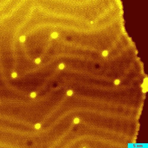
4 Atomic steps on Ag(111) Boncharduk et al., Phys.Rev.Lett. 99, (2007) 4

5 Current induced cleaning of graphene Moser, Barreiro, Bachtold, Appl.Phys.Lett. 91, (2007) 5
6 Basic concepts of electromigration F ez * d ez * w E Effective valence. For metals typically Direct force: associated with Landauer dipole 6
7 Towards microscopic understanding of current induced forces Theory is mostly phenomenological Experiments probing forces on atomic scale are almost absent 7

8 Current induced single-atom switching Schirm et al. Nature Nanotechnol. 8, 645 (2013) 8
 1 nm Tierney et al., Nature Nanotechn. 6, 625 (2011) See also: Perera et al., Nature Nanotechn. 8, 46 (2013) 9")
9 Current-induced single switching Low tunnel current (molecule not rotating) STM of molecules adsorbed to Cu(111) 1 nm Tierney et al., Nature Nanotechn. 6, 625 (2011) See also: Perera et al., Nature Nanotechn. 8, 46 (2013) 9

10 10
.")
11 Atomic water wheel D. Dundas, E.J. McEniry, T.N. Todorov, Nature Nanotechnol., 4, (2009). 11
12 The Berry force Lü, Brandbyge, Hedegård, Nano Lett. 10, 1657 (2010). The electron wavefunction ϕ depends on the positions of the ions R. Projecting out the electronic states, Leads to an effective magnetic field Semi-classical Langevin equation for the motion of ion cores 12
13 Model system: two degrees of freedom Lü, Brandbyge, Hedegård, Nano Lett. 10, 1657 (2010). 13
14 A model system: chain of Au atoms Lü, Brandbyge, Hedegård, Nano Lett. 10, 1657 (2010). 14

15 Experiments of current-induced breaking 15

16 Experiments of current-induced breaking Smit, Untiedt, van Ruitenbeek, Nanotechnol. 15, S472 (2004). 16

17 Experiments of current-induced breaking Smit, Untiedt, van Ruitenbeek, Nanotechnol. 15, S472 (2004). 17

18 Experiments of current-induced breaking Sabater, Untiedt, van Ruitenbeek, to be published 18

19 Experiments of current-induced breaking Initial stability test at 10mV Sabater, Untiedt, van Ruitenbeek, to be published 19
20 Pt chain: higher energy runaway mode 20
21 Pt chain: higher energy runaway mode 21


22 Can we do these experiments in a more controlled way? STM Tip Atomic Chain Molecule 22


23 Low-temperature STM Au (111) atomic resolution Electronic edge states The Beast 23
")
24 Deposition of single atoms by low-t evaporation Au ad-atoms over Au(111) surface 24


25 PRL 79, (1997) J. Vac. Sci. Technol., B 23(2005) Lateral manipulation of atoms STM Tip

26 Single atom manipulation: Au on Au(111) 26

27 Single atom manipulation: Au on Au(111) 27

28 Single atom manipulation: Au on Au(111) 28

29 Single atom manipulation: Au on Au(111) 29

30 Single atom manipulation: Au on Au(111) 30

31 Single atom manipulation: Au on Au(111) 31

32 Connected chain formation 32

33 Connected chain formation 33

34 Connected chain formation 34

35 Connected chain formation Three atoms chain 35
36 Single-molecule conductors 47 cycles Courtesy: Wagner C. Fournier (Tautz) et al., PRB 84, (2011) 36
 et al.")
37 Single-molecule conductors 37 Fournier (Tautz) et al., PRB 84, (2011)
38 STM Tip Building atomic conductors between tip and sample Atomic Chain 38


39 3-dimensional STM control x y z feedback Force field simulation 39
 to the tight-binding Hamiltonian Initialize program Load libraries")
 x* (V) 3D motion sensor x,y,z Move the Base atoms of tip y*(v) Relax")
 et al.")
40 Force Field Simulation Interatomic potential 1 : Second-moment approximation (SMA) to the tight-binding Hamiltonian Initialize program Load libraries Define variables and classes Load system (Tip + surface + ad atoms) Base atoms z* (V) x* (V) 3D motion sensor x,y,z Move the Base atoms of tip y*(v) Relax system for new tip position Tunnelling current feedback Visual feedback Print the new state of the system End R Cortes Huerto (Saul) et al., PRB 88, (2013)

41 Possible process suggested by simulation 41


42 STM control: The game x y z feedback Force field simulation 42


43 Can also do break junctions x y z feedback Force field simulation 43


44 The team Christian Wagner Sumit Tewari Jacob Bakermans Federica Galli Roel Smit Carlos Untiedt Carlos Sabater Tadashi Shiota Raphael Muller Marius Trouwborst Sasha Vrbica Irene Battisi Elena Tartaglini Jan Aarts Support from Sylvestre Bonnet Tchavdar Todorov Daniel Dundas Mads Brandbyge Stefan Tautz LeidenCenterUltramicroscopy 44


45 Conclusions 45

46 46
Heat and electron transport in nano-structured conductors: Insights from atomistic simulations Mads Brandbyge
 Heat and electron transport in nano-structured conductors: Insights from atomistic simulations Mads Brandbyge Dept. of micro and nanotech. & Center for Nanostructured Graphene (CNG) Technical University
Scattering theory of current-induced forces. Reinhold Egger Institut für Theoretische Physik, Univ. Düsseldorf
 Scattering theory of current-induced forces Reinhold Egger Institut für Theoretische Physik, Univ. Düsseldorf Overview Current-induced forces in mesoscopic systems: In molecule/dot with slow mechanical
Non-conservative forces in bulk systems
 Non-conservative forces in bulk systems Todorov, T. N., Cunningham, B., Dundas, D., & Horsfield, A. P. (2017). Non-conservative forces in bulk systems. Materials Science And Technology. https://doi.org/10.1080/02670836.2017.1296991
Tuning magnetic anisotropy, Kondo screening and Dzyaloshinskii-Moriya interaction in pairs of Fe adatoms
 Tuning magnetic anisotropy, Kondo screening and Dzyaloshinskii-Moriya interaction in pairs of Fe adatoms Department of Physics, Hamburg University, Hamburg, Germany SPICE Workshop, Mainz Outline Tune magnetic
STM spectroscopy (STS)
") STM spectroscopy (STS) di dv 4 e ( E ev, r) ( E ) M S F T F Basic concepts of STS. With the feedback circuit open the variation of the tunneling current due to the application of a small oscillating voltage
STM spectroscopy (STS) di dv 4 e ( E ev, r) ( E ) M S F T F Basic concepts of STS. With the feedback circuit open the variation of the tunneling current due to the application of a small oscillating voltage
Microscopical and Microanalytical Methods (NANO3)
") Microscopical and Microanalytical Methods (NANO3) 06.11.15 10:15-12:00 Introduction - SPM methods 13.11.15 10:15-12:00 STM 20.11.15 10:15-12:00 STS Erik Zupanič erik.zupanic@ijs.si stm.ijs.si 27.11.15
Microscopical and Microanalytical Methods (NANO3) 06.11.15 10:15-12:00 Introduction - SPM methods 13.11.15 10:15-12:00 STM 20.11.15 10:15-12:00 STS Erik Zupanič erik.zupanic@ijs.si stm.ijs.si 27.11.15
Molecular and carbon based electronic systems
 Molecular and carbon based electronic systems Single molecule deposition and properties on surfaces Bottom Up Top Down Fundamental Knowledge & Functional Devices Thilo Glatzel, thilo.glatzel@unibas.ch
arxiv:cond-mat/ v1 [cond-mat.mes-hall] 6 Sep 2002
![arxiv:cond-mat/ v1 [cond-mat.mes-hall] 6 Sep 2002](/thumbs/74/71316176.jpg "arxiv:cond-mat/ v1 [cond-mat.mes-hall] 6 Sep 2002") Nonlinear current-induced forces in Si atomic wires arxiv:cond-mat/963v [cond-mat.mes-hall] 6 Sep Zhongqin Yang and Massimiliano Di Ventra[*] Department of Physics, Virginia Polytechnic Institute and State
Nonlinear current-induced forces in Si atomic wires arxiv:cond-mat/963v [cond-mat.mes-hall] 6 Sep Zhongqin Yang and Massimiliano Di Ventra[*] Department of Physics, Virginia Polytechnic Institute and State
Measuring charge transport through molecules
 Measuring charge transport through molecules utline Indirect methods 1. ptical techniques 2. Electrochemical techniques Direct methods 1. Scanning probe techniques 2. In-plane electrodes 3. Break junctions
ᣂቇⴚ㗔 䇸䉮䊮䊏䊠䊷䊁䉞䉪䉴䈮䉋䉎 䊂䉱䉟䊮䋺ⶄว 㑐䈫㕖ᐔⴧ䉻䉟䊅䊚䉪䉴䇹 ᐔᚑ22ᐕᐲ ળ䇮2011ᐕ3 4ᣣ䇮 ੩ᄢቇᧄㇹ䉨䊞䊮䊌䉴 㗄 A02 ኒᐲ 㑐ᢙᴺℂ 䈮ၮ䈨䈒㕖ᐔⴧ 䊅䊉䉴䉬䊷䊦㔚 વዉ䉻䉟䊅䊚䉪䉴 ઍ ᄢᎿ ㆺ
 22201134 A02 GCOE Si device (further downsizing) Novel nanostructures (such as atomic chain) Nanoscale multi-terminal resistance measurement Carbon nanotube transistor Atomic switch Interplay:l Dynamics:
Spectroscopy at nanometer scale
 Spectroscopy at nanometer scale 1. Physics of the spectroscopies 2. Spectroscopies for the bulk materials 3. Experimental setups for the spectroscopies 4. Physics and Chemistry of nanomaterials Various
Herre van der Zant. interplay between molecular spin and electron transport (molecular spintronics) Gate
 Gate") transport through the single molecule magnet Mn12 Herre van der Zant H.B. Heersche, Z. de Groot (Delft) C. Romeike, M. Wegewijs (RWTH Aachen) D. Barreca, E. Tondello (Padova) L. Zobbi, A. Cornia (Modena)
transport through the single molecule magnet Mn12 Herre van der Zant H.B. Heersche, Z. de Groot (Delft) C. Romeike, M. Wegewijs (RWTH Aachen) D. Barreca, E. Tondello (Padova) L. Zobbi, A. Cornia (Modena)
Simple molecules as benchmark systems for molecular electronics
 Simple molecules as benchmark systems for molecular electronics 1 In collaboration with... Kamerlingh Onnes Laboratory, Leiden University Darko Djukic Yves Noat Roel Smit Carlos Untiedt & JvR Gorlaeus
Scanning Tunneling Microscopy. how does STM work? the quantum mechanical picture example of images how can we understand what we see?
 Scanning Tunneling Microscopy how does STM work? the quantum mechanical picture example of images how can we understand what we see? Observation of adatom diffusion with a field ion microscope Scanning
INTRODUCTION TO SCA\ \I\G TUNNELING MICROSCOPY
 INTRODUCTION TO SCA\ \I\G TUNNELING MICROSCOPY SECOND EDITION C. JULIAN CHEN Department of Applied Physics and Applied Mathematics, Columbia University, New York OXFORD UNIVERSITY PRESS Contents Preface
Conductance Calculations for Small Molecules
 Conductance Calculations for Small Molecules Karsten W. Jacobsen CAMP, Dept. of Physics Technical University of Denmark Outline Framework Density Functional Theory Conductance calculations methodology
Scanning Probe Microscopy (SPM)
") http://ww2.sljus.lu.se/staff/rainer/spm.htm Scanning Probe Microscopy (FYST42 / FAFN30) Scanning Probe Microscopy (SPM) overview & general principles March 23 th, 2018 Jan Knudsen, room K522, jan.knudsen@sljus.lu.se
http://ww2.sljus.lu.se/staff/rainer/spm.htm Scanning Probe Microscopy (FYST42 / FAFN30) Scanning Probe Microscopy (SPM) overview & general principles March 23 th, 2018 Jan Knudsen, room K522, jan.knudsen@sljus.lu.se
Single-Molecule Junctions: Vibrational and Magnetic Degrees of Freedom, and Novel Experimental Techniques
 Single-Molecule Junctions: Vibrational and Magnetic Degrees of Freedom, and Novel Experimental Techniques Heiko B. Weber Lehrstuhl für Angewandte Physik Friedrich-Alexander-Universität Erlangen-Nürnberg
From manipulation of the charge state to imaging of individual molecular orbitals and bond formation
 Scanning Probe Microscopy of Adsorbates on Insulating Films: From manipulation of the charge state to imaging of individual molecular orbitals and bond formation Gerhard Meyer, Jascha Repp, Peter Liljeroth
Raman spectroscopy study of rotated double-layer graphene: misorientation angle dependence of electronic structure
 Supplementary Material for Raman spectroscopy study of rotated double-layer graphene: misorientation angle dependence of electronic structure Kwanpyo Kim 1,2,3, Sinisa Coh 1,3, Liang Z. Tan 1,3, William
Exploring the Interatomic Forces between Tip and Single Molecules during STM Manipulation
 Exploring the Interatomic Forces between Tip and Single Molecules during STM Manipulation NANO LETTERS 2006 Vol. 6, No. 12 2685-2689 Leonhard Grill,* Karl-Heinz Rieder, and Francesca Moresco Institut für
QS School Summary
 2018 NSF/DOE/AFOSR Quantum Science Summer School June 22, 2018 QS 3 2018 School Summary Kyle Shen (Cornell) Some Thank yous! A Big Thanks to Caroline Brockner!!! Also to our fantastic speakers! Kavli Institute
Spatially resolving density-dependent screening around a single charged atom in graphene
 Supplementary Information for Spatially resolving density-dependent screening around a single charged atom in graphene Dillon Wong, Fabiano Corsetti, Yang Wang, Victor W. Brar, Hsin-Zon Tsai, Qiong Wu,
2) Atom manipulation. Xe / Ni(110) Model: Experiment:
 Atom manipulation. Xe / Ni(110) Model: Experiment:") 2) Atom manipulation D. Eigler & E. Schweizer, Nature 344, 524 (1990) Xe / Ni(110) Model: Experiment: G.Meyer, et al. Applied Physics A 68, 125 (1999) First the tip is approached close to the adsorbate
2) Atom manipulation D. Eigler & E. Schweizer, Nature 344, 524 (1990) Xe / Ni(110) Model: Experiment: G.Meyer, et al. Applied Physics A 68, 125 (1999) First the tip is approached close to the adsorbate
Chapter 103 Spin-Polarized Scanning Tunneling Microscopy
 Chapter 103 Spin-Polarized Scanning Tunneling Microscopy Toyo Kazu Yamada Keywords Spin-polarized tunneling current Spin polarization Magnetism 103.1 Principle Spin-polarized scanning tunneling microscopy
Spin electric coupling and coherent quantum control of molecular nanomagnets
 Spin electric coupling and coherent quantum control of molecular nanomagnets Dimitrije Stepanenko Department of Physics University of Basel Institute of Physics, Belgrade February 15. 2010 Collaborators:
SUPPLEMENTARY INFORMATION
 Simultaneous and coordinated rotational switching of all molecular rotors in a network Y. Zhang, H. Kersell, R. Stefak, J. Echeverria, V. Iancu, U. G. E. Perera, Y. Li, A. Deshpande, K.-F. Braun, C. Joachim,
In the name of Allah
 In the name of Allah Nano chemistry- 4 th stage Lecture No. 1 History of nanotechnology 16-10-2016 Assistance prof. Dr. Luma Majeed Ahmed lumamajeed2013@gmail.com, luma.ahmed@uokerbala.edu.iq Nano chemistry-4
Apparent Barrier Height in Scanning Tunneling Microscopy Revisited
 Downloaded from orbit.dtu.dk on: Nov 05, 2018 Apparent Barrier Height in Scanning Tunneling Microscopy Revisited Olesen, L.; Brandbyge, Mads; Sørensen, Mads Reinholdt; Jacobsen, Karsten Wedel; Lægsgaard,
Modeling inelastic phonon scattering in atomic- and molecular-wire junctions
 Downloaded from orbit.dtu.dk on: Mar 10, 2019 Modeling inelastic phonon scattering in atomic- and molecular-wire junctions Paulsson, Magnus; Frederiksen, Thomas; Brandbyge, Mads Published in: Physical
Electron transport through molecular junctions and FHI-aims
 STM m metallic surface Electron transport through molecular junctions and FHI-aims Alexei Bagrets Inst. of Nanotechnology (INT) & Steinbuch Centre for Computing (SCC) @ Karlsruhe Institute of Technology
Supplementary information for Probing atomic structure and Majorana wavefunctions in mono-atomic Fe chains on superconducting Pb surface
 Supplementary information for Probing atomic structure and Majorana wavefunctions in mono-atomic Fe chains on superconducting Pb surface Rémy Pawlak 1, Marcin Kisiel 1, Jelena Klinovaja 1, Tobias Meier
An ab initio approach to electrical transport in molecular devices
 INSTITUTE OF PHYSICSPUBLISHING Nanotechnology 13 (00) 1 4 An ab initio approach to electrical transport in molecular devices NANOTECHNOLOGY PII: S0957-4484(0)31500-9 JJPalacios 1,ELouis 1,AJPérez-Jiménez,ESanFabián
Chapter 5 Nanomanipulation. Chapter 5 Nanomanipulation. 5.1: With a nanotube. Cutting a nanotube. Moving a nanotube
 Objective: learn about nano-manipulation techniques with a STM or an AFM. 5.1: With a nanotube Moving a nanotube Cutting a nanotube Images at large distance At small distance : push the NT Voltage pulse
Spectroscopies for Unoccupied States = Electrons
 Spectroscopies for Unoccupied States = Electrons Photoemission 1 Hole Inverse Photoemission 1 Electron Tunneling Spectroscopy 1 Electron/Hole Emission 1 Hole Absorption Will be discussed with core levels
Apparent reversal of molecular orbitals reveals entanglement
 Apparent reversal of molecular orbitals reveals entanglement Andrea Donarini P.Yu, N. Kocic, B.Siegert, J.Repp University of Regensburg and Shanghai Tech University Entangled ground state Spectroscopy
Surface Transfer Doping of Diamond by Organic Molecules
 Surface Transfer Doping of Diamond by Organic Molecules Qi Dongchen Department of Physics National University of Singapore Supervisor: Prof. Andrew T. S. Wee Dr. Gao Xingyu Scope of presentation Overview
The basics of Scanning Probe Microscopy
 McGill University, Montreal, Jan. 8 th 2009 The basics of Scanning Probe Microscopy Federico Rosei Canada Research Chair in Nanostructured Organic and Inorganic Materials Énergie, Matériaux et Télécommunications,
Graphite, graphene and relativistic electrons
 Graphite, graphene and relativistic electrons Introduction Physics of E. graphene Y. Andrei Experiments Rutgers University Transport electric field effect Quantum Hall Effect chiral fermions STM Dirac
Energy band of manipulated atomic structures on an insulator substrate
 Energy band of manipulated atomic structures on an insulator substrate Toshishige Yamada and Yoshihisa Yamamoto ERATO Quantum Fluctuation Project, Edward L. Ginzton Laboratory, Stanford University, Stanford,
Measurement of Current-Induced Local Heating in a Single Molecule Junction
 Measurement of Current-Induced Local Heating in a Single Molecule Junction NANO LETTERS 2006 Vol. 6, No. 6 1240-1244 Zhifeng Huang, Bingqian Xu, Yuchang Chen, Massimiliano Di Ventra,*, and Nongjian Tao*,
Langevin approach to non-adiabatic molecular dynamics
 Langevin approach to non-adiabatic molecular dynamics Jing Tao Lü 1, Mads Brandbyge 1, Per Hedegård 2 1. Department of Micro- and Nanotechnology, Technical University of Denmark 2. Niels Bohr institute,
Many-body correlations in STM single molecule junctions
 Many-body correlations in STM single molecule junctions Andrea Donarini Institute of Theoretical Physics, University of Regensburg, Germany TMSpin Donostia Many-body correlations in STM single molecule
Many-body correlations in a Cu-phthalocyanine STM single molecule junction
 Many-body correlations in a Cu-phthalocyanine STM single molecule junction Andrea Donarini Institute of Theoretical Physics, University of Regensburg (Germany) Organic ligand Metal center Non-equilibrium
STM spectra of graphene
 STM spectra of graphene K. Sengupta Theoretical Physics Division, IACS, Kolkata. Collaborators G. Baskaran, I.M.Sc Chennai, K. Saha, IACS Kolkata I. Paul, Grenoble France H. Manoharan, Stanford USA Refs:
High-temperature single-electron transistor based on a gold nanoparticle
 High-temperature single-electron transistor based on a gold nanoparticle SA Dagesyan 1 *, A S Stepanov 2, E S Soldatov 1, G Zharik 1 1 Lomonosov Moscow State University, faculty of physics, Moscow, Russia,
In situ studies on dynamic properties of carbon nanotubes with metal clusters
 In situ studies on dynamic properties of carbon nanotubes with metal clusters Jason Chang, Yuan-Chih Chang, Der-Hsien Lien, Shaw-Chieh Wang*, Tung Hsu*, and Tien T. Tsong Institute of Physics, Academia
Visualization of atomic-scale phenomena in superconductors
 Visualization of atomic-scale phenomena in superconductors Andreas Kreisel, Brian Andersen Niels Bohr Institute, University of Copenhagen, 2100 København, Denmark Peayush Choubey, Peter Hirschfeld Department
J 12 J 23 J 34. Driving forces in the nano-magnetism world. Intra-atomic exchange, electron correlation effects: Inter-atomic exchange: MAGNETIC ORDER
 Driving forces in the nano-magnetism world Intra-atomic exchange, electron correlation effects: LOCAL (ATOMIC) MAGNETIC MOMENTS m d or f electrons Inter-atomic exchange: MAGNETIC ORDER H exc J S S i j
Concepts in Surface Physics
 M.-C. Desjonqueres D. Spanjaard Concepts in Surface Physics Second Edition With 257 Figures Springer 1. Introduction................................. 1 2. Thermodynamical and Statistical Properties of
1. Robust hexagonal rings on Cu(111) Figure S1 2. Details of Monte Carlo simulations
 Figure S1 2. Details of Monte Carlo simulations") Supporting Information for Influence of Relativistic Effects on Assembled Structures of V-Shaped Bispyridine Molecules on M(111) Surfaces where M = Cu, Ag, Au Xue Zhang, 1,ǁ Na Li, 1, Hao Wang, 1 Chenyang
Supporting Information for Influence of Relativistic Effects on Assembled Structures of V-Shaped Bispyridine Molecules on M(111) Surfaces where M = Cu, Ag, Au Xue Zhang, 1,ǁ Na Li, 1, Hao Wang, 1 Chenyang
Surface Characte i r i zat on LEED Photoemission Phot Linear optics
 Surface Characterization i LEED Photoemission Linear optics Surface characterization with electrons MPS M.P. Seah, WA W.A. Dench, Surf. Interf. Anal. 1 (1979) 2 LEED low energy electron diffraction De
Molecular Electronics
 Molecular Electronics An Introduction to Theory and Experiment Juan Carlos Cuevas Universidad Autönoma de Madrid, Spain Elke Scheer Universität Konstanz, Germany 1>World Scientific NEW JERSEY LONDON SINGAPORE
Supplementary Information:
 Supplementary Figures Supplementary Information: a b 1 2 3 0 ΔZ (pm) 66 Supplementary Figure 1. Xe adsorbed on a Cu(111) surface. (a) Scanning tunnelling microscopy (STM) topography of Xe layer adsorbed
Scanning Tunneling Microscopy
 Scanning Tunneling Microscopy Scanning Direction References: Classical Tunneling Quantum Mechanics Tunneling current Tunneling current I t I t (V/d)exp(-Aφ 1/2 d) A = 1.025 (ev) -1/2 Å -1 I t = 10 pa~10na
METAL/CARBON-NANOTUBE INTERFACE EFFECT ON ELECTRONIC TRANSPORT
 METAL/CARBON-NANOTUBE INTERFACE EFFECT ON ELECTRONIC TRANSPORT S. Krompiewski Institute of Molecular Physics, Polish Academy of Sciences, M. Smoluchowskiego 17, 60-179 Poznań, Poland OUTLINE 1. Introductory
Carbon Nanotubes in Interconnect Applications
 Carbon Nanotubes in Interconnect Applications Page 1 What are Carbon Nanotubes? What are they good for? Why are we interested in them? - Interconnects of the future? Comparison of electrical properties
tunneling theory of few interacting atoms in a trap
 tunneling theory of few interacting atoms in a trap Massimo Rontani CNR-NANO Research Center S3, Modena, Italy www.nano.cnr.it Pino D Amico, Andrea Secchi, Elisa Molinari G. Maruccio, M. Janson, C. Meyer,
ICTP Conference Graphene Week 2008
 1960-3 ICTP Conference Graphene Week 2008 25-29 August 2008 Current-induced cleaning of graphene J. Moser CIN2 Barcelona, Campus UAB, Bellaterra, Spain A. Barreiro CIN2 Barcelona, Campus UAB, Bellaterra,
Dimerized & frustrated spin chains. Application to copper-germanate
 Dimerized & frustrated spin chains Application to copper-germanate Outline CuGeO & basic microscopic models Excitation spectrum Confront theory to experiments Doping Spin-Peierls chains A typical S=1/2
Hartmut Buhmann. Physikalisches Institut, EP3 Universität Würzburg Germany
 Hartmut Buhmann Physikalisches Institut, EP3 Universität Würzburg Germany Part I and II Insulators and Topological Insulators HgTe crystal structure Part III quantum wells Two-Dimensional TI Quantum Spin
From exhaustive simulations to key principles in DNA nanoelectronics
 From exhaustive simulations to key principles in DNA nanoelectronics Dvira Segal Department of Chemistry University of Toronto Roman Korol (undergrad) Hyehwang Kim (undergrad) Michael Kilgour (grad) Challenge:
Momentum filtering effect in molecular wires
 PHYSICAL REVIEW B 70, 195309 (2004) Momentum filtering effect in molecular wires Chao-Cheng Kaun, 1, * Hong Guo, 1 Peter Grütter, 1 and R. Bruce Lennox 1,2 1 Center for the Physics of Materials and Department
The Trapping and Characterization of a Single Hydrogen. Molecule in a Continuously Tunable Nanocavity
 The Trapping and Characterization of a Single Hydrogen Molecule in a Continuously Tunable Nanocavity Hui Wang 1,2,+, Shaowei Li 2, Haiyan He 2,3,+, Arthur Yu 2, Freddy Toledo 4, Zhumin Han 2, W. Ho 2,4,*
X-ray Imaging and Spectroscopy of Individual Nanoparticles
 X-ray Imaging and Spectroscopy of Individual Nanoparticles A. Fraile Rodríguez, F. Nolting Swiss Light Source Paul Scherrer Institut, Switzerland Intensity [a.u.] 1.4 1.3 1.2 1.1 D 8 nm 1 1 2 3 1.0 770
Heat transfer in ultrahigh vacuum scanning thermal microscopy
 Heat transfer in ultrahigh vacuum scanning thermal microscopy W. Müller-Hirsch, a) A. Kraft, M. T. Hirsch, J. Parisi, and A. Kittel Department of Energy and Semiconductor Research, Faculty of Physics,
Fabrication and Measurement of Spin Devices. Purdue Birck Presentation
 Fabrication and Measurement of Spin Devices Zhihong Chen School of Electrical and Computer Engineering Birck Nanotechnology Center, Discovery Park Purdue University Purdue Birck Presentation zhchen@purdue.edu
Magnetic Nanowires inside. carbon nanotubes
 Leibniz Institute for Solid State and Materials Research IFW Dresden Magnetic Nanowires inside Carbon Nanotubes Magnetic force microscopy sensors using ironfilled carbon nanotubes Thomas Mühl Outline Introduction
Büttiker s probe in molecular electronics: Applications to charge and heat transport
 Büttiker s probe in molecular electronics: Applications to charge and heat transport Dvira Segal Department of Chemistry University of Toronto Michael Kilgour (poster) Büttiker s probe in molecular electronics:
Electronic Properties of Atomic Wires: from Semiconductor Surfaces to Organic Chains and DNA. F. J. Himpsel
 Electronic Properties of Atomic Wires: from Semiconductor Surfaces to Organic Chains and DNA F. J. Himpsel One-dimensional phenomena Ultimate limit of nanowires, electronics Single chain of overlapping
Scanning Tunneling Microscopy
 Scanning Tunneling Microscopy References: 1. G. Binnig, H. Rohrer, C. Gerber, and Weibel, Phys. Rev. Lett. 49, 57 (1982); and ibid 50, 120 (1983). 2. J. Chen, Introduction to Scanning Tunneling Microscopy,
Outline. Introduction: graphene. Adsorption on graphene: - Chemisorption - Physisorption. Summary
 Outline Introduction: graphene Adsorption on graphene: - Chemisorption - Physisorption Summary 1 Electronic band structure: Electronic properties K Γ M v F = 10 6 ms -1 = c/300 massless Dirac particles!
Zero- or two-dimensional?
 Stacked layers of submonolayer InAs in GaAs: Zero- or two-dimensional? S. Harrison*, M. Young, M. Hayne, P. D. Hodgson, R. J. Young A. Schliwa, A. Strittmatter, A. Lenz, H. Eisele, U. W. Pohl, D. Bimberg
Mesoscopic Spintronics
 Mesoscopic Spintronics Taro WAKAMURA (Université Paris-Sud) Lecture 1 Today s Topics 1.1 History of Spintronics 1.2 Fudamentals in Spintronics Spin-dependent transport GMR and TMR effect Spin injection
Experimental methods in physics. Local probe microscopies I
 Experimental methods in physics Local probe microscopies I Scanning tunnelling microscopy (STM) Jean-Marc Bonard Academic year 09-10 1. Scanning Tunneling Microscopy 1.1. Introduction Image of surface
Coulomb blockade and single electron tunnelling
 Coulomb blockade and single electron tunnelling Andrea Donarini Institute of theoretical physics, University of Regensburg Three terminal device Source System Drain Gate Variation of the electrostatic
Hydrogen Storage in Metalfunctionalized
 Hydrogen Storage in Metalfunctionalized Graphene Stefan Heun NEST, Istituto Nanoscienze-CNR and Scuola Normale Superiore Pisa, Italy Outline Introduction to Hydrogen Storage Epitaxial Graphene Hydrogen
Adiabatic quantum motors
 Felix von Oppen Freie Universität Berlin with Raul Bustos Marun and Gil Refael Motion at the nanoscale Brownian motion Directed motion at the nanoscale?? 2 Directed motion at the nanoscale Nanocars 3 Nanoscale
Transport through Andreev Bound States in a Superconductor-Quantum Dot-Graphene System
 Transport through Andreev Bound States in a Superconductor-Quantum Dot-Graphene System Nadya Mason Travis Dirk, Yung-Fu Chen, Cesar Chialvo Taylor Hughes, Siddhartha Lal, Bruno Uchoa Paul Goldbart University
Interaction between a single-molecule
 Interaction between a single-molecule magnet Mn 12 monolayer and a gold surface 12 Kyungwha Park Department of Physics, Virginia Tech Salvador Barraza-Lopez (postdoc) Michael C. Avery (undergraduate) Supported
arxiv:cond-mat/ v1 [cond-mat.mes-hall] 19 Nov 2003
![arxiv:cond-mat/ v1 [cond-mat.mes-hall] 19 Nov 2003](/thumbs/73/69001878.jpg "arxiv:cond-mat/ v1 [cond-mat.mes-hall] 19 Nov 2003") High-bias stability of monatomic chains arxiv:cond-mat/311439v1 [cond-mat.mes-hall] 19 Nov 3 R.H.M. Smit, 1 C. Untiedt, 1,2 and J.M. van Ruitenbeek 1 1 Kamerlingh Onnes Laboratorium, Universiteit Leiden,
High-bias stability of monatomic chains arxiv:cond-mat/311439v1 [cond-mat.mes-hall] 19 Nov 3 R.H.M. Smit, 1 C. Untiedt, 1,2 and J.M. van Ruitenbeek 1 1 Kamerlingh Onnes Laboratorium, Universiteit Leiden,
Scanning probe microscopy of graphene with a CO terminated tip
 Scanning probe microscopy of graphene with a CO terminated tip Andrea Donarini T. Hofmann, A. J. Weymouth, F. Gießibl 7.5.2014 - Theory Group Seminar The sample Single monolayer of graphene Epitaxial growth
Micro & nano-cooling: electronic cooling and thermometry based on superconducting tunnel junctions
 Micro & nano-cooling: electronic cooling and thermometry based on superconducting tunnel junctions Hervé Courtois Néel Institute, CNRS and Université Joseph Fourier, Grenoble, France with L. Pascal, H.
Scanning Tunneling Microscopy: theory and examples
 Scanning Tunneling Microscopy: theory and examples Jan Knudsen The MAX IV laboratory & Division of synchrotron radiation research K5-53 (Sljus) jan.knudsen@sljus.lu.se April 17, 018 http://www.sljus.lu.se/staff/rainer/spm.htm
Introduction to Scanning Probe Microscopy Zhe Fei
 Introduction to Scanning Probe Microscopy Zhe Fei Phys 590B, Apr. 2019 1 Outline Part 1 SPM Overview Part 2 Scanning tunneling microscopy Part 3 Atomic force microscopy Part 4 Electric & Magnetic force
arxiv: v1 [cond-mat.mes-hall] 16 Nov 2007
![arxiv: v1 [cond-mat.mes-hall] 16 Nov 2007](/thumbs/93/112291523.jpg "arxiv: v1 [cond-mat.mes-hall] 16 Nov 2007") Transport properties of graphene nanoribbon arxiv:7.6v [cond-mat.mes-hall] 6 Nov 7 heterostructures L. Rosales a,, P. Orellana b, Z. Barticevic a, M.Pacheco a a Departamento de Física, Universidad Técnica
Transport properties of graphene nanoribbon arxiv:7.6v [cond-mat.mes-hall] 6 Nov 7 heterostructures L. Rosales a,, P. Orellana b, Z. Barticevic a, M.Pacheco a a Departamento de Física, Universidad Técnica
Scanning Tunneling Microscopy/Spectroscopy
 Scanning Tunneling Microscopy/Spectroscopy 0 Scanning Tunneling Microscope 1 Scanning Tunneling Microscope 2 Scanning Tunneling Microscope 3 Typical STM talk or paper... The differential conductance di/dv
Scanning Tunneling Microscopy Studies of the Ge(111) Surface
 Surface") VC Scanning Tunneling Microscopy Studies of the Ge(111) Surface Anna Rosen University of California, Berkeley Advisor: Dr. Shirley Chiang University of California, Davis August 24, 2007 Abstract: This
VC Scanning Tunneling Microscopy Studies of the Ge(111) Surface Anna Rosen University of California, Berkeley Advisor: Dr. Shirley Chiang University of California, Davis August 24, 2007 Abstract: This
Energy Spectroscopy. Ex.: Fe/MgO
 Energy Spectroscopy Spectroscopy gives access to the electronic properties (and thus chemistry, magnetism,..) of the investigated system with thickness dependence Ex.: Fe/MgO Fe O Mg Control of the oxidation
Atomic and molecular interactions. Scanning probe microscopy.
 Atomic and molecular interactions. Scanning probe microscopy. Balázs Kiss Nanobiotechnology and Single Molecule Research Group, Department of Biophysics and Radiation Biology 27. November 2013. 2 Atomic
Investigation on the growth of CNTs from SiO x and Fe 2 O 3 nanoparticles by in situ TEM
 The 5 th Workshop on Nucleation and Growth Mechanisms of SWCNTs Investigation on the growth of CNTs from SiO x and Fe 2 O 3 nanoparticles by in situ TEM Chang Liu Shenyang National Laboratory for Materials
Nanomaterials Electrical and Optical Properties
 Nanomaterials Electrical and Optical Properties H.Hofmann ÉCOLE POLYTECHNIQUE FÉDÉRALE DE LAUSANNE Electrical Properties Energy LUMO HOMO Forbidden bandgap Atom Mo lecule Cluster Nanoparticle Semi conductor
Molecular Dynamics on the Angstrom Scale
 Probing Interface Reactions by STM: Molecular Dynamics on the Angstrom Scale Zhisheng Li Prof. Richard Osgood Laboratory for Light-Surface Interactions, Columbia University Outline Motivation: Why do we
Don Eigler IBM Fellow. Spin Excitation Spectroscopy : A Tool Set For Nano-Scale Spin Systems
 Don Eigler IBM Fellow Spin Excitation Spectroscopy : A Tool Set For Nano-Scale Spin Systems NSF Grantees Conference, Arlington, VA. December 6, 2010 A Challenge Build a Spin-Only Nano-Scale Digital Computer
Quantum-Chemical Interpretation of Current-Induced Forces on Adatoms on Carbon Nanotubes
 12478 J. Phys. Chem. C 2007, 111, 12478-12482 Quantum-Chemical Interpretation of Current-Induced Forces on Adatoms on Carbon Nanotubes Yvan Girard,* Takahiro Yamamoto, and Kazuyuki Watanabe Department
Nanoelectronics 09. Atsufumi Hirohata Department of Electronics. Quick Review over the Last Lecture
 Nanoelectronics 09 Atsufumi Hirohata Department of Electronics 13:00 Monday, 12/February/2018 (P/T 006) Quick Review over the Last Lecture ( Field effect transistor (FET) ): ( Drain ) current increases
Lithography-free Fabrication of High Quality Substrate-supported and. Freestanding Graphene devices
 Lithography-free Fabrication of High Quality Substrate-supported and Freestanding Graphene devices W. Bao 1, G. Liu 1, Z. Zhao 1, H. Zhang 1, D. Yan 2, A. Deshpande 3, B.J. LeRoy 3 and C.N. Lau 1, * 1
Graphene Nanoribbons: A Route to Atomically Precise Nanoelectronics Mike Crommie
 Graphene Nanoribbons: A Route to Atomically Precise Nanoelectronics Mike Crommie Dept. of Physics, UC Berkeley and Materials Science Division, LBNL Berkeley, CA Outline 1) Graphene Graphene Nanoribbon
Manipulation of interface-induced Skyrmions studied with STM
 Manipulation of interface-induced Skyrmions studied with STM Kirsten von Bergmann S. Heinze, M. Bode, P. Ferriani, E.Y. Vedmedenko, A. Kubetzka, O. Pietzsch and R. Wiesendanger Institute of Applied Physics,,
Branislav K. Nikolić
 First-principles quantum transport modeling of thermoelectricity in nanowires and single-molecule nanojunctions Branislav K. Nikolić Department of Physics and Astronomy, University of Delaware, Newark,