Chapter 9 The introduction of EELS EELS principle
|
|
|
- Milo Alexander
- 5 years ago
- Views:
Transcription
1 Chapter 9 The introduction of EELS EELS principle (Chap. 37, 38, 39, 40) Textbook: R.F. Egerton, Electron Energy-Loss Spectroscopy in the Electron Microscope, 2nd edition
2 Particle picture of scattering elastic inner-shell inelastic outer-shell inelastic
3 TEM beam-specimen interactions and signals
4 What is EELS - Electron Energy Loss Spectroscopy EEL spectrum is collected series energy loss electrons which generated with the inelastic scattering collision with specimen Energy after inelastic scattering incident electron energy Specimen absorption energy

5 Atomic-scale view of electron energy loss in TEM Energy and Momentum Conservation of scattering process
6 valence or conduction band energy-band diagram

7 Core ionization edges and the core level diagram
8

9 Electron Bean E 0 Positive ion cores Incident electron NTHU Plasmon oscillation Free electron gas Energy loss TEM Column Energy-loss electron E 0 -ΔE P E 0 Energy-Filter Spectrum Energy slit Image E 0 -ΔE P E 0
10 Ray Tracing for a 90 degree magnetic Sector Spectrometer
 Parallel EELS (e.g. Gatan 666) Gatan Enfina Gatan")
11 EELS instrumentation spectrum/imaging Below the TEM: Serial EELS (e.g. Gatan 607) Parallel EELS (e.g. Gatan 666) Gatan Enfina Gatan Imaging Filter In-column: Prism-mirror (Leo) Omega Filter (Leo, JEOL)
12 A magnetic prism bends, disperses and focuses an electron beam e v B = F =mv 2 /R R = (m/e)(v/b) R

13 Gatan Image Filter (GIF)

14 Leo-922 energy-filtering TEM omega filter
15 Omega-filter in-column spectrometer (Four magnetic prisms) After objective lens Diffraction pattern o real or virtual image of specimen real or virtual image of specimen energy-selecting slit Before projector lens Diffraction pattern D2 is conjugated with D1 optical axis
16 The EELS looks like Zero loss Low loss region Core loss region band gap dielectric constant
17 EELS spectral information dσ/dedω=4γ 2 /a o q 4 Σ i,j <f q.r i> δ(e+e f -E i )~M 2 ρ(r) NTHU Plasma loss Dielectric Function Band gap Bandgap Interband transition (Valence->Conduction) Thickness Interband transition (valence-> conduction band) Core loss: electronic structure unoccupied-dos atomic environment
18 Jellium Model The resonant motion of electron gas would be self-sustaining if there were no damping from the atomic lattice. The displacement x of a quasi-free electron (effective mass m) due to a local electric field E must satisfy the equation of motion. for a oscillatory field m x + mγ x = ee E = E exp( iωt) The displacement has a solution given by x = (ee /m)(ω 2 + iγω) 1 18
19 The displacement x give rise to a polarization P P = enx = ε o χe χis the electronic susceptibility and n is the number of electrons per unit volume The relative permittivity or dielectric function ε(ω)=1+χ is then given by 2 ω ε(ω) = ε 1 + iε 2 =1 p ω 2 + Γ + 2 ω p ω p = (ne 2 /(ε o m)) 1/ 2 2 iγω p ω(γ 2 + Γ 2 ) is the plasmon frequency (the frequency ε1 passes through 0) The energy loss function is defined as Im[ 1 ε(ω) ] = ε 2 ε ε 2 2 = 2 ωγω p (ω 2 ω 2 p ) 2 + (ωγ) 2
20 Drude Model for Volume Plasmon For RuO 2 a=b=0.449 nm, c=0.31 nm (one unit cell has 2Ru and 4O) Ru : [Kr]4d 7 5s =8 O : [He]2s 2 2p 4 =6 # of free electrons = 40=2x(8+2x6) è While m= x10-31 kg e= x10-19 C ε 0 =10 7 /4πc 2 =8.842x ev= x10-19 J
21 Plasmon loss from RuO2 nanowires

22 Correlating electron energy levels with EELS edges Unoccupied state 2p3/2 >3d5/3 2p1/2 >3d2/3
23 Energy-loss spectrum (log-intensity) of YBCO
24
25
26 Band Structure of Si Conduction Band EF Valence Band 26
27 27
28
29
30
31 What EELS can do Typically applied to: * measurement of specimen thickness * analysis of elemental composition * phase identification via signature in EELS fine structure Also applicable to studies of: * electronic band structure and chemical bonding * atom-specific near-neighbor distributions (RDF) * Band gap analysis for optoelectronic material * dielectric response, ε(ω,q)
32 Measurement of specimen thickness t/λ = ln(i t /I 0 ) λ ~ 100 nm but depends on Z, E 0 and β Value obtained from calibration specimen or from tables (for common materials) or from parameterized formula
33 EELS fine structure (Egerton and Whelan, 1974) CB1 CB2 plural π* σ*
34 K-edge spectra of diamond and grain from the Allende meteorite (Blake et al., Nature 332, 1988, 611) π*


35 Oxidation state of Cr in a bacterium (Daulton et al, M&M 7, 479, 2001)
36 Compare the EELS and EDX technique Prior to the 1980, most EDX detector were protected (from the water vapor and hydrocarbon in the microscope column) by a 10µm thickness beryllium window, which strongly absorbs photons of energy less than 1000eV and percludes analysis of elements of atomic number less than 11. With development of ultrathin (UTW) or atmosphericpressure (ATW), elements down to boron can be routinely detected, making EDX competitive with EELS for microanalysis of light elements in a TEM specimen. 36
37 EELS and x-ray Signal Generation
38 X-ray fluorescence yield (log scale) as a function of atomic number atomic number
39 The EELS is one step signal, while EDX is a two step signal (low x-ray fluorescence yield for low Z). In general, the yield rate of the EELS is higher than EDX. the signal of EELS concentrates in a small angle range of the transmitted beam, but the EDX signal spans around larger angle range. (a) These two cause EELS has higher core loss signal (higher Signal to noise ratio, EELS has less recording time)
40 (b) EDX has better Signal/ background ratio Background of EELS: arises from the inelastic scattering from the atomic electron whose binding energy less than the edge energy Background of EDX: arises from bremsstrahlung
 beam broaden size")
41 u The beam broaden effect EDX bulk beam broaden size for SEM system EDX thin film (TEM) beam broaden size
42 (c)x-ray has larger interaction volume than that of electron. The ultimate spatial resolution is higher for EELS than for EDX, but the thin crystal is required for EELS Broaden by elastic scattering of x-ray limited by the accept angle
43 Beam broaden formula: density The EDX spatial resolution limit Energy of Indicate electron beam The EDX spatial resolution ( R ) equation: For example: Specimen thickness :100nm, b is about 10nm Nano EDX Beam size (d) :0.5 nm The resolution limit: R=5.25 nm atomic weight
44 Follow previous slice, the beta angle for EDX is about 0.82 rad=820mrad For EELS image mode, the beta angle is about mrad For example: The beam size is about 0.5nm; specimen thickness is about 100nm The EDX beam R max is 5.256nm EELS R max is about 0.6nm de-localization of energy loss electron
45 (d) EELS is an absolute, standardless quantitation technique, but quantification error may exist in the case of crystal. (e) Structural information is available, but more operator intensive is required. 45
46 (f) Comparison of EELS and XEDS sensitivity (depends on strongly on SNR, but not SBR) (Leapman et al.) EELS is capable of detecting smaller concentrations of elements of low atomic number
47 (g) EDX resolution is ev so there is peak overlap below 1000eV EELS resolution is ~ 1 ev so edge overlap can be less (stainless steel, Zaluzec 1984)
48 EELS vs. EDXS


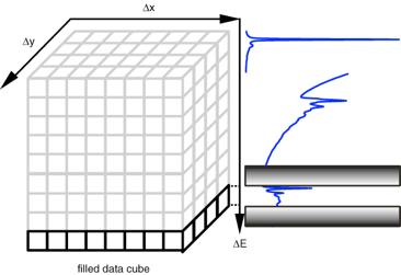
49 擷取可以定量分析之三維空間 EELS 訊息 I(x,y, ΔE) STEM EFTEM NTHU

50 What is EFTEM - Energy Filtering Transmission Electron Microscopy
51 The features of EFTEM A contrast-enhancement technique: it improves contrast in images and diffraction patterns by removing inelastically scattered electrons that produce background fog. A mapping technique: it creates elemental maps by forming images with inelastically scattered electrons. An analytical technique: it records and quantifies electron energy-loss spectra to provide precise chemical analysis of TEM samples.

52 The standard EFTEM elemental mapping images

 Si")
53 銅製程與低介電常數材料已是半導體元件發展趨勢 0.13µm 乃 至於 90nm 的製程技術 NTHU 如何在具有圖案結構上之試 片決定介電材質之介電常數 Cross-sectional TEM image Copper Dielectric layer B Diameter: (8 inches) Si Substrate Copper Dual-Damascene Structure
54 傳統之介電常數量測 Al electrode Dielectric layer( t d,ε ) Si substrate ~ A V DC NTHU 利 用的 MOS Capacitor 結構來量測其 C-V 曲線得到電容值反推得到介電層之介電常數值 V DC = t C d d 數 ) ε 0 ( ε 0 : 真空介電常 因此對於有結構圖案之試 片無法使 用此 方法量測介電層之介電常數值


55 影像能譜 (ESI) 之擷取 Dielectric Function Imaging NTHU x 71 images BD A ΔE Counts 71 data channels Si 3 N 4 SiO 2 Si Extract imagespectrum from a nm 2 area y Electron Energy Loss (ev)

56 B NTHU A
 ε1 9eV 22 Black")

57 Dielectric Function image Black Diamond Si 3 N 4 Y NTHU -10 SiO 2 Si 18 nm 0eV X 3eV 6eV Electron energy Loss (ev) ε1 9eV 22 Black Diamond Y -10 Si 3 N 4 SiO 2 X Si nm 0eV 2eV 4eV 6.5eV 9eV Lo, Chen, L. Chang and Kai et al., Journal of electron Microscopy (2000) ε2

58 介電常數分佈影像圖 (dielectric constant map) B l a c k Diamond Si 3 N 4 SiO Dielectric constant NTHU Materials ε ε SiO ±0.31 Si 3 N ±0.30 Black Diamond TM 2.5~ ±0.27 Si 50 nm 4.6
59 Band gap energy Imaging J 1 2 ( E) M ρ( E) = ( E ) Bruley and Brown ( parabolic band ) E g a NTHU M: transition Matrix from Valence band to conduction band ρ(e): Density of state of condution band J 1 (E) : a = 0.5 a=1.5 ( direct band gap ) ( in-direct band gap )

60 AlN/GaN Quantum Well EDX B A GaN AlN GaN AlN NTHU GaN/AlN multilayers were grown on Si substrate by MBE EELS TEM image GaN AlN Al-L edge EELS spectra AlN GaN AlN Series ESI images ΔE


61 Band Gap Map NTHU The map of band energy of AlN/GaN layers is obtained using electron spectroscopy imaging (ESI) technique. The average band-gap energy of AlN and GaN is determined to be about 5.62 ± 0.35 ev and 3.47 ± 0.36 ev, respectively. AlN GaN AlN AlN GaN AlNGaN AlN Tsai, Kai,Chen,L. Chang, Journal of Electron Microscopy (2003)

 ] specimen")
![area(π * ) [ area(π * + σ * ) ]](/docs-images/82/85618448/images/62-4.jpg "reference Yan, Kai, Chen,L.")
62 Chemical Bonding sp 2 /sp 3 Map EELS element Map sp 2 /sp 3 Map NTHU NiP 5 nm area(π * ) [ area(π f sp 2 = * + σ * ) ] specimen area(π * ) [ area(π * + σ * ) ] reference Yan, Kai, Chen,L. Chang, JEM (2002)


63 Structure of the specimen NTHU α-fe 2 O 3 Fe Cu Si Substrate(100) α-fe 2 O 3 Fe Cu Znoe axis(10-10)


64 Image to Spectrum X Fe NTHU α-fe 2 O 3 specimen 5 nm Energy axis From 646eV~742eV Y Y


65 Valence State Mapping NTHU Cu Fe α-fe 2 O 3 Fe Cu α-fe 2 O 3
Chemical Analysis in TEM: XEDS, EELS and EFTEM. HRTEM PhD course Lecture 5
 Chemical Analysis in TEM: XEDS, EELS and EFTEM HRTEM PhD course Lecture 5 1 Part IV Subject Chapter Prio x-ray spectrometry 32 1 Spectra and mapping 33 2 Qualitative XEDS 34 1 Quantitative XEDS 35.1-35.4
Chapter 22 Lecture. Essential University Physics Richard Wolfson 2 nd Edition. Electric Potential 電位 Pearson Education, Inc.
 Chapter 22 Lecture Essential University Physics Richard Wolfson 2 nd Edition Electric Potential 電位 Slide 22-1 In this lecture you ll learn 簡介 The concept of electric potential difference 電位差 Including
B k k. Fig. 1: Energy-loss spectrum of BN, showing the how K-loss intensities I K (β, ) for boron and nitrogen are defined and measured.
 for boron and nitrogen are defined and measured.") The accuracy of EELS elemental analysis The procedure of EELS elemental analysis can be divided into three parts, each of which involves some approximation, with associated systematic or statistical errors.
The accuracy of EELS elemental analysis The procedure of EELS elemental analysis can be divided into three parts, each of which involves some approximation, with associated systematic or statistical errors.
KMÜ 396 MATERIALS SCIENCE AND TECH. I PRESENTATION ELECTRON ENERGY LOSS SPECTROSCOPY (EELS) TUĞÇE SEZGİN
 TUĞÇE SEZGİN") KMÜ 396 MATERIALS SCIENCE AND TECH. I PRESENTATION ELECTRON ENERGY LOSS SPECTROSCOPY (EELS) TUĞÇE SEZGİN 20970725 HACETTEPE UNIVERSITY DEPARTMENT OF CHEMICAL ENGINEERING, SPRING 2011,APRIL,ANKARA CONTENTS
KMÜ 396 MATERIALS SCIENCE AND TECH. I PRESENTATION ELECTRON ENERGY LOSS SPECTROSCOPY (EELS) TUĞÇE SEZGİN 20970725 HACETTEPE UNIVERSITY DEPARTMENT OF CHEMICAL ENGINEERING, SPRING 2011,APRIL,ANKARA CONTENTS
6. Analytical Electron Microscopy
 Physical Principles of Electron Microscopy 6. Analytical Electron Microscopy Ray Egerton University of Alberta and National Institute of Nanotechnology Edmonton, Canada www.tem-eels.ca regerton@ualberta.ca
CHAPTER 2. Energy Bands and Carrier Concentration in Thermal Equilibrium
 CHAPTER 2 Energy Bands and Carrier Concentration in Thermal Equilibrium 光電特性 Ge 被 Si 取代, 因為 Si 有較低漏電流 Figure 2.1. Typical range of conductivities for insulators, semiconductors, and conductors. Figure
Electron and electromagnetic radiation
 Electron and electromagnetic radiation Generation and interactions with matter Stimuli Interaction with sample Response Stimuli Waves and energy The energy is propotional to 1/λ and 1/λ 2 λ λ 1 Electromagnetic
0 0 = 1 0 = 0 1 = = 1 1 = 0 0 = 1
 0 0 = 1 0 = 0 1 = 0 1 1 = 1 1 = 0 0 = 1 : = {0, 1} : 3 (,, ) = + (,, ) = + + (, ) = + (,,, ) = ( + )( + ) + ( + )( + ) + = + = = + + = + = ( + ) + = + ( + ) () = () ( + ) = + + = ( + )( + ) + = = + 0
Chapter 6. Series-Parallel Circuits ISU EE. C.Y. Lee
 Chapter 6 Series-Parallel Circuits Objectives Identify series-parallel relationships Analyze series-parallel circuits Determine the loading effect of a voltmeter on a circuit Analyze a Wheatstone bridge
Transmission Electron Microscopy
 L. Reimer H. Kohl Transmission Electron Microscopy Physics of Image Formation Fifth Edition el Springer Contents 1 Introduction... 1 1.1 Transmission Electron Microscopy... 1 1.1.1 Conventional Transmission
生物統計教育訓練 - 課程. Introduction to equivalence, superior, inferior studies in RCT 謝宗成副教授慈濟大學醫學科學研究所. TEL: ext 2015
 生物統計教育訓練 - 課程 Introduction to equivalence, superior, inferior studies in RCT 謝宗成副教授慈濟大學醫學科學研究所 tchsieh@mail.tcu.edu.tw TEL: 03-8565301 ext 2015 1 Randomized controlled trial Two arms trial Test treatment
= lim(x + 1) lim x 1 x 1 (x 2 + 1) 2 (for the latter let y = x2 + 1) lim
 lim x 1 x 1 (x 2 + 1) 2 (for the latter let y = x2 + 1) lim") 1061 微乙 01-05 班期中考解答和評分標準 1. (10%) (x + 1)( (a) 求 x+1 9). x 1 x 1 tan (π(x )) (b) 求. x (x ) x (a) (5 points) Method without L Hospital rule: (x + 1)( x+1 9) = (x + 1) x+1 x 1 x 1 x 1 x 1 (x + 1) (for the
1061 微乙 01-05 班期中考解答和評分標準 1. (10%) (x + 1)( (a) 求 x+1 9). x 1 x 1 tan (π(x )) (b) 求. x (x ) x (a) (5 points) Method without L Hospital rule: (x + 1)( x+1 9) = (x + 1) x+1 x 1 x 1 x 1 x 1 (x + 1) (for the
and Electron Energy Loss spectroscopy Bo Yang A Dissertation Presented in Partial Fulfillment of the Requirements for the Degree Doctor of Philosophy
 Functional Materials characterizations by Scanning/Transmission Electron Microscopy and Electron Energy Loss spectroscopy by Bo Yang A Dissertation Presented in Partial Fulfillment of the Requirements
IMAGING DIFFRACTION SPECTROSCOPY
 TEM Techniques TEM/STEM IMAGING DIFFRACTION SPECTROSCOPY Amplitude contrast (diffracion contrast) Phase contrast (highresolution imaging) Selected area diffraction Energy dispersive X-ray spectroscopy
Elastic and Inelastic Scattering in Electron Diffraction and Imaging
 Elastic and Inelastic Scattering in Electron Diffraction and Imaging Contents Introduction Symbols and definitions Part A Diffraction and imaging of elastically scattered electrons Chapter 1. Basic kinematical
Review of Optical Properties of Materials
 Review of Optical Properties of Materials Review of optics Absorption in semiconductors: qualitative discussion Derivation of Optical Absorption Coefficient in Direct Semiconductors Photons When dealing
Ch.9 Liquids and Solids
 Ch.9 Liquids and Solids 9.1. Liquid-Vapor Equilibrium 1. Vapor Pressure. Vapor Pressure versus Temperature 3. Boiling Temperature. Critical Temperature and Pressure 9.. Phase Diagram 1. Sublimation. Melting
Introduction to X-ray Photoelectron Spectroscopy (XPS) XPS which makes use of the photoelectric effect, was developed in the mid-1960
 XPS which makes use of the photoelectric effect, was developed in the mid-1960") Introduction to X-ray Photoelectron Spectroscopy (XPS) X-ray Photoelectron Spectroscopy (XPS), also known as Electron Spectroscopy for Chemical Analysis (ESCA) is a widely used technique to investigate
Introduction to X-ray Photoelectron Spectroscopy (XPS) X-ray Photoelectron Spectroscopy (XPS), also known as Electron Spectroscopy for Chemical Analysis (ESCA) is a widely used technique to investigate
MT Electron microscopy Scanning electron microscopy and electron probe microanalysis
 MT-0.6026 Electron microscopy Scanning electron microscopy and electron probe microanalysis Eero Haimi Research Manager Outline 1. Introduction Basics of scanning electron microscopy (SEM) and electron
Electron Microscopy I
 Characterization of Catalysts and Surfaces Characterization Techniques in Heterogeneous Catalysis Electron Microscopy I Introduction Properties of electrons Electron-matter interactions and their applications
Dr. Tao Li
 Tao Li taoli@nju.edu.cn Nat. Lab. of Solid State Microstructures Department of Materials Science and Engineering Nanjing University Concepts Basic principles Surface Plasmon Metamaterial Summary Light
Energy-Filtering. Transmission. Electron Microscopy
 Part 3 Energy-Filtering Transmission Electron Microscopy 92 Energy-Filtering TEM Principle of EFTEM expose specimen to mono-energetic electron radiation inelastic scattering in the specimen poly-energetic
Lecture 3: Optical Properties of Insulators, Semiconductors, and Metals. 5 nm
 Metals Lecture 3: Optical Properties of Insulators, Semiconductors, and Metals 5 nm Course Info Next Week (Sept. 5 and 7) no classes First H/W is due Sept. 1 The Previous Lecture Origin frequency dependence
EELS Electron Energy Loss Spectroscopy
 EELS Electron Energy Loss Spectroscopy (Thanks to Steve Pennycook, Quan Li, Charlie Lyman, Ondre Krivenak, David Muller, David Bell, Natasha Erdman, Nestor Zaluzec and many others) Nestor Zaluzec,
EELS, Surface Plasmon and Adsorbate Vibrations
 EELS, Surface Plasmon and Adsorbate Vibrations Ao Teng 2010.10.11 Outline I. Electron Energy Loss Spectroscopy(EELS) and High Resolution EELS (HREELS) II. Surface Plasmon III. Adsorbate Vibrations Surface
EXPERMENT 9. To determination of Quinine by fluorescence spectroscopy. Introduction
 EXPERMENT 9 To determination of Quinine by fluorescence spectroscopy Introduction Many chemical compounds can be excited by electromagnetic radication from normally a singlet ground state S o to upper
Techniques EDX, EELS et HAADF en TEM: possibilités d analyse et applications
 Techniques EDX, EELS et HAADF en TEM: possibilités d analyse et applications Thomas Neisius Université Paul Cézanne Plan Imaging modes HAADF Example: supported Pt nanoparticles Electron sample interaction
Gaetano L Episcopo. Scanning Electron Microscopy Focus Ion Beam and. Pulsed Plasma Deposition
 Gaetano L Episcopo Scanning Electron Microscopy Focus Ion Beam and Pulsed Plasma Deposition Hystorical background Scientific discoveries 1897: J. Thomson discovers the electron. 1924: L. de Broglie propose
Chapter 20 Cell Division Summary
 Chapter 20 Cell Division Summary Bk3 Ch20 Cell Division/1 Table 1: The concept of cell (Section 20.1) A repeated process in which a cell divides many times to make new cells Cell Responsible for growth,
Core-Level spectroscopy. Experiments and first-principles calculations. Tomoyuki Yamamoto. Waseda University, Japan
 Core-Level spectroscopy Experiments and first-principles calculations Tomoyuki Yamamoto Waseda University, Japan 22 nd WIEN2k workshop Jun. 26 th, 2015@Singapore Outline What is core-level spectroscopy
X-Ray Photoelectron Spectroscopy (XPS)-2
-2") X-Ray Photoelectron Spectroscopy (XPS)-2 Louis Scudiero http://www.wsu.edu/~scudiero; 5-2669 Fulmer 261A Electron Spectroscopy for Chemical Analysis (ESCA) The 3 step model: 1.Optical excitation 2.Transport
X-Ray Photoelectron Spectroscopy (XPS)-2 Louis Scudiero http://www.wsu.edu/~scudiero; 5-2669 Fulmer 261A Electron Spectroscopy for Chemical Analysis (ESCA) The 3 step model: 1.Optical excitation 2.Transport
Chapter 9. Electron mean free path Microscopy principles of SEM, TEM, LEEM
 Chapter 9 Electron mean free path Microscopy principles of SEM, TEM, LEEM 9.1 Electron Mean Free Path 9. Scanning Electron Microscopy (SEM) -SEM design; Secondary electron imaging; Backscattered electron
Chapter 8 Lecture. Essential University Physics Richard Wolfson 2 nd Edition. Gravity 重力 Pearson Education, Inc. Slide 8-1
 Chapter 8 Lecture Essential University Physics Richard Wolfson 2 nd Edition Gravity 重力 Slide 8-1 In this lecture you ll learn 簡介 Newton s law of universal gravitation 萬有引力 About motion in circular and
2.57/2.570 Midterm Exam No. 1 April 4, :00 am -12:30 pm
 Name:.57/.570 Midterm Exam No. April 4, 0 :00 am -:30 pm Instructions: ().57 students: try all problems ().570 students: Problem plus one of two long problems. You can also do both long problems, and one
MSE 321 Structural Characterization
 Auger Spectroscopy Auger Electron Spectroscopy (AES) Scanning Auger Microscopy (SAM) Incident Electron Ejected Electron Auger Electron Initial State Intermediate State Final State Physical Electronics
Lecture 7 Light-Matter Interaction Part 1 Basic excitation and coupling. EECS Winter 2006 Nanophotonics and Nano-scale Fabrication P.C.
 Lecture 7 Light-Matter Interaction Part 1 Basic excitation and coupling EECS 598-00 Winter 006 Nanophotonics and Nano-scale Fabrication P.C.Ku What we have learned? Nanophotonics studies the interaction
Praktikum zur. Materialanalytik
 Praktikum zur Materialanalytik Energy Dispersive X-ray Spectroscopy B513 Stand: 19.10.2016 Contents 1 Introduction... 2 2. Fundamental Physics and Notation... 3 2.1. Alignments of the microscope... 3 2.2.
Studying Metal to Insulator Transitions in Solids using Synchrotron Radiation-based Spectroscopies.
 PY482 Lecture. February 28 th, 2013 Studying Metal to Insulator Transitions in Solids using Synchrotron Radiation-based Spectroscopies. Kevin E. Smith Department of Physics Department of Chemistry Division
IV. Surface analysis for chemical state, chemical composition
 IV. Surface analysis for chemical state, chemical composition Probe beam Detect XPS Photon (X-ray) Photoelectron(core level electron) UPS Photon (UV) Photoelectron(valence level electron) AES electron
The Dielectric Function of a Metal ( Jellium )
") The Dielectric Function of a Metal ( Jellium ) Total reflection Plasma frequency p (10 15 Hz range) Why are Metals Shiny? An electric field cannot exist inside a metal, because metal electrons follow the
The Dielectric Function of a Metal ( Jellium ) Total reflection Plasma frequency p (10 15 Hz range) Why are Metals Shiny? An electric field cannot exist inside a metal, because metal electrons follow the
MT Electron microscopy Scanning electron microscopy and electron probe microanalysis
 MT-0.6026 Electron microscopy Scanning electron microscopy and electron probe microanalysis Eero Haimi Research Manager Outline 1. Introduction Basics of scanning electron microscopy (SEM) and electron
MSE 321 Structural Characterization
 Auger Spectroscopy Auger Electron Spectroscopy (AES) Scanning Auger Microscopy (SAM) Incident Electron Ejected Electron Auger Electron Initial State Intermediate State Final State Physical Electronics
Frequency Response (Bode Plot) with MATLAB
 with MATLAB") Frequency Response (Bode Plot) with MATLAB 黃馨儀 216/6/15 適應性光子實驗室 常用功能選單 File 選單上第一個指令 New 有三個選項 : M-file Figure Model 開啟一個新的檔案 (*.m) 用以編輯 MATLAB 程式 開始一個新的圖檔 開啟一個新的 simulink 檔案 Help MATLAB Help 查詢相關函式 MATLAB
Frequency Response (Bode Plot) with MATLAB 黃馨儀 216/6/15 適應性光子實驗室 常用功能選單 File 選單上第一個指令 New 有三個選項 : M-file Figure Model 開啟一個新的檔案 (*.m) 用以編輯 MATLAB 程式 開始一個新的圖檔 開啟一個新的 simulink 檔案 Help MATLAB Help 查詢相關函式 MATLAB
X-Ray Photoelectron Spectroscopy (XPS)-2
-2") X-Ray Photoelectron Spectroscopy (XPS)-2 Louis Scudiero http://www.wsu.edu/~pchemlab ; 5-2669 Fulmer 261A Electron Spectroscopy for Chemical Analysis (ESCA) The 3 step model: 1.Optical excitation 2.Transport
X-Ray Photoelectron Spectroscopy (XPS)-2 Louis Scudiero http://www.wsu.edu/~pchemlab ; 5-2669 Fulmer 261A Electron Spectroscopy for Chemical Analysis (ESCA) The 3 step model: 1.Optical excitation 2.Transport
Structural characterization. Part 1
 Structural characterization Part 1 Experimental methods X-ray diffraction Electron diffraction Neutron diffraction Light diffraction EXAFS-Extended X- ray absorption fine structure XANES-X-ray absorption
Optical Properties of Solid from DFT
 Optical Properties of Solid from DFT 1 Prof.P. Ravindran, Department of Physics, Central University of Tamil Nadu, India & Center for Materials Science and Nanotechnology, University of Oslo, Norway http://folk.uio.no/ravi/cmt15
壓差式迴路式均熱片之研製 Fabrication of Pressure-Difference Loop Heat Spreader
 壓差式迴路式均熱片之研製 Fabrication of Pressure-Difference Loop Heat Spreader 1 2* 3 4 4 Yu-Tang Chen Shei Hung-Jung Sheng-Hong Tsai Shung-Wen Kang Chin-Chun Hsu 1 2* 3! "# $ % 4& '! " ( )* +, -. 95-2622-E-237-001-CC3
Overview of scattering, diffraction & imaging in the TEM
 Overview of scattering, diffraction & imaging in the TEM Eric A. Stach Purdue University Scattering Electrons, photons, neutrons Radiation Elastic Mean Free Path (Å)( Absorption Length (Å)( Minimum Probe
Electron-Matter Interactions
 Electron-Matter Interactions examples of typical EM studies properties of electrons elastic electron-matter interactions scattering processes; coherent and incoherent image formation; chemical contrast;
Multiple sequence alignment (MSA)
") Multiple sequence alignment (MSA) From pairwise to multiple A T _ A T C A... A _ C A T _ A... A T _ G C G _... A _ C G T _ A... A T C A C _ A... _ T C G A G A... Relationship of sequences (Tree) NODE
Multiple sequence alignment (MSA) From pairwise to multiple A T _ A T C A... A _ C A T _ A... A T _ G C G _... A _ C G T _ A... A T C A C _ A... _ T C G A G A... Relationship of sequences (Tree) NODE
Nanoelectronics 09. Atsufumi Hirohata Department of Electronics. Quick Review over the Last Lecture
 Nanoelectronics 09 Atsufumi Hirohata Department of Electronics 13:00 Monday, 12/February/2018 (P/T 006) Quick Review over the Last Lecture ( Field effect transistor (FET) ): ( Drain ) current increases
Lecture 20 Optical Characterization 2
 Lecture 20 Optical Characterization 2 Schroder: Chapters 2, 7, 10 1/68 Announcements Homework 5/6: Is online now. Due Wednesday May 30th at 10:00am. I will return it the following Wednesday (6 th June).
Single Electron Transistor
 Single-Electron Transistors u Reference book: Single Charge Tunneling Coulomb Blockade Phenomena in Nanostructures By Hermann Grabertand Michel H. Devoret, 1992 u Referred Journal Review Papers: Correlated
Chapter 1 Linear Regression with One Predictor Variable
 Chapter 1 Linear Regression with One Predictor Variable 許湘伶 Applied Linear Regression Models (Kutner, Nachtsheim, Neter, Li) hsuhl (NUK) LR Chap 1 1 / 41 Regression analysis is a statistical methodology
SEM. Chemical Analysis in the. Elastic and Inelastic scattering. Chemical analysis in the SEM. Chemical analysis in the SEM
 THE UNIVERSITY Chemical Analysis in the SEM Ian Jones Centre for Electron Microscopy OF BIRMINGHAM Elastic and Inelastic scattering Electron interacts with one of the orbital electrons Secondary electrons,
Understanding X-rays: The electromagnetic spectrum
 Understanding X-rays: The electromagnetic spectrum 1 ULa 13.61 kev 0.09 nm BeKa 0.11 kev 11.27 nm E = hn = h c l where, E : energy, h : Planck's constant, n : frequency c : speed of light in vacuum, l
Lecture 5. X-ray Photoemission Spectroscopy (XPS)
") Lecture 5 X-ray Photoemission Spectroscopy (XPS) 5. Photoemission Spectroscopy (XPS) 5. Principles 5.2 Interpretation 5.3 Instrumentation 5.4 XPS vs UV Photoelectron Spectroscopy (UPS) 5.5 Auger Electron
Lecture 5 X-ray Photoemission Spectroscopy (XPS) 5. Photoemission Spectroscopy (XPS) 5. Principles 5.2 Interpretation 5.3 Instrumentation 5.4 XPS vs UV Photoelectron Spectroscopy (UPS) 5.5 Auger Electron
Energy-Filtered High-Resolution Electron Microscopy for Quantitative Solid State Structure Determination
 [J. Res. Natl. Inst. Stand. Technol. 102, 1 (1997)] Energy-Filtered High-Resolution Electron Microscopy for Quantitative Solid State Structure Determination Volume 102 Number 1 January February 1997 Z.
1 dx (5%) andˆ x dx converges. x2 +1 a
 andˆ x dx converges. x2 +1 a") 微甲 - 班期末考解答和評分標準. (%) (a) (7%) Find the indefinite integrals of secθ dθ.) d (5%) and + d (%). (You may use the integral formula + (b) (%) Find the value of the constant a for which the improper integral
微甲 - 班期末考解答和評分標準. (%) (a) (7%) Find the indefinite integrals of secθ dθ.) d (5%) and + d (%). (You may use the integral formula + (b) (%) Find the value of the constant a for which the improper integral
High-Resolution. Transmission. Electron Microscopy
 Part 4 High-Resolution Transmission Electron Microscopy 186 Significance high-resolution transmission electron microscopy (HRTEM): resolve object details smaller than 1nm (10 9 m) image the interior of
Concepts in Surface Physics
 M.-C. Desjonqueres D. Spanjaard Concepts in Surface Physics Second Edition With 257 Figures Springer 1. Introduction................................. 1 2. Thermodynamical and Statistical Properties of
Plasmonics. The long wavelength of light ( μm) creates a problem for extending optoelectronics into the nanometer regime.
 creates a problem for extending optoelectronics into the nanometer regime.") Plasmonics The long wavelength of light ( μm) creates a problem for extending optoelectronics into the nanometer regime. A possible way out is the conversion of light into plasmons. They have much shorter
Plasmonics The long wavelength of light ( μm) creates a problem for extending optoelectronics into the nanometer regime. A possible way out is the conversion of light into plasmons. They have much shorter
Interactions with Matter
 Manetic Lenses Manetic fields can displace electrons Manetic field can be produced by passin an electrical current throuh coils of wire Manetic field strenth can be increased by usin a soft ferromanetic
EDS User School. Principles of Electron Beam Microanalysis
 EDS User School Principles of Electron Beam Microanalysis Outline 1.) Beam-specimen interactions 2.) EDS spectra: Origin of Bremsstrahlung and characteristic peaks 3.) Moseley s law 4.) Characteristic
Type of bonds. Four general categories bonds 2. ionic 3. covalent 4. Vander Waals
 Type of bonds Four general categories bonds 1.metallic 2. ionic 3. covalent 4. Vander Waals Primary bond is commonly applied to metallic type. ionic covalent ~100 kcal/mol Secondary bonds : Vander Waals
Spectroscopy at nanometer scale
 Spectroscopy at nanometer scale 1. Physics of the spectroscopies 2. Spectroscopies for the bulk materials 3. Experimental setups for the spectroscopies 4. Physics and Chemistry of nanomaterials Various
Bandgap engineering through nanocrystalline magnetic alloy grafting on. graphene
 Electronic Supplementary Material (ESI) for Physical Chemistry Chemical Physics. This journal is the Owner Societies 2014 Electronic Supplementary Information (ESI) for Bandgap engineering through nanocrystalline
頁數 (Page): 2 of 12 測試結果 (Test Results) 測試部位 (PART NAME)No.1 : 銅色片狀 (COPPER COLORED SHEET) 測試項目 (Test Items) 單位 (Unit) 測試方法 (Method) 方法偵測極限值 (MDL) 結果 (
: 2 of 12 測試結果 (Test Results) 測試部位 (PART NAME)No.1 : 銅色片狀 (COPPER COLORED SHEET) 測試項目 (Test Items) 單位 (Unit) 測試方法 (Method) 方法偵測極限值 (MDL) 結果 (") 頁數 (Page): 1 of 12 以下測試樣品係由申請廠商所提供及確認 (The following sample(s) was/were submitted and identified by/on behalf of the applicant as): 樣品名稱 (Sample Description) 樣品型號 (Style/Item No.) 收件日期 (Sample Receiving
頁數 (Page): 1 of 12 以下測試樣品係由申請廠商所提供及確認 (The following sample(s) was/were submitted and identified by/on behalf of the applicant as): 樣品名稱 (Sample Description) 樣品型號 (Style/Item No.) 收件日期 (Sample Receiving
Algorithms and Complexity
 Algorithms and Complexity 2.1 ALGORITHMS( 演算法 ) Def: An algorithm is a finite set of precise instructions for performing a computation or for solving a problem The word algorithm algorithm comes from the
X-Ray Photoelectron Spectroscopy (XPS)
") X-Ray Photoelectron Spectroscopy (XPS) Louis Scudiero http://www.wsu.edu/~scudiero; 5-2669 Fulmer 261A Electron Spectroscopy for Chemical Analysis (ESCA) The basic principle of the photoelectric effect
X-Ray Photoelectron Spectroscopy (XPS) Louis Scudiero http://www.wsu.edu/~scudiero; 5-2669 Fulmer 261A Electron Spectroscopy for Chemical Analysis (ESCA) The basic principle of the photoelectric effect
相關分析. Scatter Diagram. Ch 13 線性迴歸與相關分析. Correlation Analysis. Correlation Analysis. Linear Regression And Correlation Analysis
 Ch 3 線性迴歸與相關分析 相關分析 Lear Regresso Ad Correlato Aalyss Correlato Aalyss Correlato Aalyss Correlato Aalyss s the study of the relatoshp betwee two varables. Scatter Dagram A Scatter Dagram s a chart that
Methods of surface analysis
 Methods of surface analysis Nanomaterials characterisation I RNDr. Věra Vodičková, PhD. Surface of solid matter: last monoatomic layer + absorbed monolayer physical properties are effected (crystal lattice
Infrared Reflectivity Spectroscopy of Optical Phonons in Short-period AlGaN/GaN Superlattices
 Infrared Reflectivity Spectroscopy of Optical Phonons in Short-period AlGaN/GaN Superlattices J. B. Herzog, A. M. Mintairov, K. Sun, Y. Cao, D. Jena, J. L. Merz. University of Notre Dame, Dept. of Electrical
2019 年第 51 屆國際化學奧林匹亞競賽 國內初選筆試 - 選擇題答案卷
 2019 年第 51 屆國際化學奧林匹亞競賽 國內初選筆試 - 選擇題答案卷 一 單選題 :( 每題 3 分, 共 72 分 ) 題號 1 2 3 4 5 6 7 8 答案 B D D A C B C B 題號 9 10 11 12 13 14 15 16 答案 C E D D 送分 E A B 題號 17 18 19 20 21 22 23 24 答案 D A E C A C 送分 B 二 多選題
Surface Sensitivity & Surface Specificity
 Surface Sensitivity & Surface Specificity The problems of sensitivity and detection limits are common to all forms of spectroscopy. In its simplest form, the question of sensitivity boils down to whether
MECHANICS OF MATERIALS
 CHAPTER 2 MECHANICS OF MATERIALS Ferdinand P. Beer E. Russell Johnston, Jr. John T. DeWolf David F. Mazurek Lecture Notes: J. Walt Oler Texas Tech University Stress and Strain Axial Loading 2.1 An Introduction
Advanced Engineering Mathematics 長榮大學科工系 105 級
 工程數學 Advanced Engineering Mathematics 長榮大學科工系 5 級 姓名 : 學號 : 工程數學 I 目錄 Part I: Ordinary Differential Equations (ODE / 常微分方程式 ) Chapter First-Order Differential Equations ( 一階 ODE) 3 Chapter Second-Order
Linear Regression. Applied Linear Regression Models (Kutner, Nachtsheim, Neter, Li) hsuhl (NUK) SDA Regression 1 / 34
 hsuhl (NUK) SDA Regression 1 / 34") Linear Regression 許湘伶 Applied Linear Regression Models (Kutner, Nachtsheim, Neter, Li) hsuhl (NUK) SDA Regression 1 / 34 Regression analysis is a statistical methodology that utilizes the relation between
Linear Regression 許湘伶 Applied Linear Regression Models (Kutner, Nachtsheim, Neter, Li) hsuhl (NUK) SDA Regression 1 / 34 Regression analysis is a statistical methodology that utilizes the relation between
X-Ray Photoelectron Spectroscopy (XPS)
") X-Ray Photoelectron Spectroscopy (XPS) Louis Scudiero http://www.wsu.edu/~scudiero; 5-2669 Electron Spectroscopy for Chemical Analysis (ESCA) The basic principle of the photoelectric effect was enunciated
X-Ray Photoelectron Spectroscopy (XPS) Louis Scudiero http://www.wsu.edu/~scudiero; 5-2669 Electron Spectroscopy for Chemical Analysis (ESCA) The basic principle of the photoelectric effect was enunciated
Generation of X-Rays in the SEM specimen
 Generation of X-Rays in the SEM specimen The electron beam generates X-ray photons in the beam-specimen interaction volume beneath the specimen surface. Some X-ray photons emerging from the specimen have
Photon Interaction. Spectroscopy
 Photon Interaction Incident photon interacts with electrons Core and Valence Cross Sections Photon is Adsorbed Elastic Scattered Inelastic Scattered Electron is Emitted Excitated Dexcitated Stöhr, NEXAPS
sgsp agsp W=20nm W=50nm Re(n eff (e) } Re{E z Im{E x Supplementary Figure 1: Gap surface plasmon modes in MIM waveguides.
 } Re{E z Im{E x Supplementary Figure 1: Gap surface plasmon modes in MIM waveguides.") (a) 2.4 (b) (c) W Au y Electric field (a.u) x SiO 2 (d) y Au sgsp x Energy (ev) 2. 1.6 agsp W=5nm W=5nm 1.2 1 2 3 4.1.1 1 1 Re(n eff ) -1-5 5 1 x (nm) W = 2nm E = 2eV Im{E x } Re{E z } sgsp Electric field
(a) 2.4 (b) (c) W Au y Electric field (a.u) x SiO 2 (d) y Au sgsp x Energy (ev) 2. 1.6 agsp W=5nm W=5nm 1.2 1 2 3 4.1.1 1 1 Re(n eff ) -1-5 5 1 x (nm) W = 2nm E = 2eV Im{E x } Re{E z } sgsp Electric field
4. Inelastic Scattering
 1 4. Inelastic Scattering Some inelastic scattering processes A vast range of inelastic scattering processes can occur during illumination of a specimen with a highenergy electron beam. In principle, many
X-Ray Emission and Absorption
 X-Ray Emission and Absorption Author: Mike Nill Alex Bryant February 6, 20 Abstract X-rays were produced by two bench-top diffractometers using a copper target. Various nickel filters were placed in front
Statistical Intervals and the Applications. Hsiuying Wang Institute of Statistics National Chiao Tung University Hsinchu, Taiwan
 and the Applications Institute of Statistics National Chiao Tung University Hsinchu, Taiwan 1. Confidence Interval (CI) 2. Tolerance Interval (TI) 3. Prediction Interval (PI) Example A manufacturer wanted
論文與專利寫作暨學術 倫理期末報告 班級 : 碩化一甲學號 :MA 姓名 : 林郡澤老師 : 黃常寧
 論文與專利寫作暨學術 倫理期末報告 班級 : 碩化一甲學號 :MA540117 姓名 : 林郡澤老師 : 黃常寧 About 85% of the world s energy requirements are currently satisfied by exhaustible fossil fuels that have detrimental consequences on human health
Probing Matter: Diffraction, Spectroscopy and Photoemission
 Probing Matter: Diffraction, Spectroscopy and Photoemission Anders Nilsson Stanford Synchrotron Radiation Laboratory Why X-rays? VUV? What can we hope to learn? 1 Photon Interaction Incident photon interacts
Transmission Electron Microscopy and Diffractometry of Materials
 Brent Fultz James Howe Transmission Electron Microscopy and Diffractometry of Materials Fourth Edition ~Springer 1 1 Diffraction and the X-Ray Powder Diffractometer 1 1.1 Diffraction... 1 1.1.1 Introduction
Chapter 13 Thin-layer chromatography. Shin-Hun Juang, Ph.D.
 Chapter 13 Thin-layer chromatography Shin-Hun Juang, Ph.D. 1 Principles An analyte migrates up or across a layer of stationary phase (most commonly silica gel), under the influence of a mobile phase (usually
STM: Scanning Tunneling Microscope
 STM: Scanning Tunneling Microscope Basic idea STM working principle Schematic representation of the sample-tip tunnel barrier Assume tip and sample described by two infinite plate electrodes Φ t +Φ s =
Photoelectron spectroscopy Instrumentation. Nanomaterials characterization 2
 Photoelectron spectroscopy Instrumentation Nanomaterials characterization 2 RNDr. Věra V Vodičkov ková,, PhD. Photoelectron Spectroscopy general scheme Impact of X-ray emitted from source to the sample
EE 527 MICROFABRICATION. Lecture 5 Tai-Chang Chen University of Washington
 EE 527 MICROFABRICATION Lecture 5 Tai-Chang Chen University of Washington MICROSCOPY AND VISUALIZATION Electron microscope, transmission electron microscope Resolution: atomic imaging Use: lattice spacing.
授課大綱 課號課程名稱選別開課系級學分 結果預視
 授課大綱 課號課程名稱選別開課系級學分 B06303A 流體力學 Fluid Mechanics 必 結果預視 課程介紹 (Course Description): 機械工程學系 三甲 3 在流體力學第一課的學生可能會問 : 什麼是流體力學? 為什麼我必須研究它? 我為什麼要研究它? 流體力學有哪些應用? 流體包括液體和氣體 流體力學涉及靜止和運動時流體的行為 對流體力學的基本原理和概念的了解和理解對分析任何工程系統至關重要,
Spectroscopies for Unoccupied States = Electrons
 Spectroscopies for Unoccupied States = Electrons Photoemission 1 Hole Inverse Photoemission 1 Electron Tunneling Spectroscopy 1 Electron/Hole Emission 1 Hole Absorption Will be discussed with core levels
Optical Properties of Semiconductors. Prof.P. Ravindran, Department of Physics, Central University of Tamil Nadu, India
 Optical Properties of Semiconductors 1 Prof.P. Ravindran, Department of Physics, Central University of Tamil Nadu, India http://folk.uio.no/ravi/semi2013 Light Matter Interaction Response to external electric
Optical and Photonic Glasses. Lecture 39. Non-Linear Optical Glasses III Metal Doped Nano-Glasses. Professor Rui Almeida
 Optical and Photonic Glasses : Non-Linear Optical Glasses III Metal Doped Nano-Glasses Professor Rui Almeida International Materials Institute For New Functionality in Glass Lehigh University Metal-doped
EMISSION SPECTROSCOPY
 IFM The Department of Physics, Chemistry and Biology LAB 57 EMISSION SPECTROSCOPY NAME PERSONAL NUMBER DATE APPROVED I. OBJECTIVES - Understand the principle of atomic emission spectra. - Know how to acquire
PHYS-E0541:Special Course in Physics Gas phase synthesis of carbon nanotubes for thin film application. Electron Microscopy. for
 PHYS-E0541:Special Course in Physics Gas phase synthesis of carbon nanotubes for thin film application Electron Microscopy for Introduction to Electron Microscopy Carbon Nanomaterials (nanotubes) Dr. Hua
X-Ray Photoelectron Spectroscopy (XPS) Prof. Paul K. Chu
 Prof. Paul K. Chu") X-Ray Photoelectron Spectroscopy (XPS) Prof. Paul K. Chu X-ray Photoelectron Spectroscopy Introduction Qualitative analysis Quantitative analysis Charging compensation Small area analysis and XPS imaging
X-Ray Photoelectron Spectroscopy (XPS) Prof. Paul K. Chu X-ray Photoelectron Spectroscopy Introduction Qualitative analysis Quantitative analysis Charging compensation Small area analysis and XPS imaging
雷射原理. The Principle of Laser. 授課教授 : 林彥勝博士 Contents
 雷射原理 The Principle of Laser 授課教授 : 林彥勝博士 E-mail: yslin@mail.isu.edu.tw Contents Energy Level( 能階 ) Spontaneous Emission( 自發輻射 ) Stimulated Emission( 受激發射 ) Population Inversion( 居量反轉 ) Active Medium( 活性介質