Nanophysics: MENA5010/9010
|
|
|
- Philip Leonard
- 5 years ago
- Views:
Transcription
1 Nanophysics: MENA5010/9010 The course is organized by Department of Physics, UiO Lecturer: Spring 2018 Pavlo Mikheenko, University of Oslo Lectures on physics of nanostructures Student presentations (will be graded and form a part of exam) Introduction 1
2 Pavlo Mikheenko ndex.html Physics building, Room FV404 Direct/Voice Mail: 22 8(5 7471) Lecture plan and lectures: Introduction 2
3 Richard Feynman 29th December 1959 on APS Meeting at Caltech: There is plenty of room at the bottom Introduction MENA5010/9010 Spring Introduction 3

4 Syllabus The purpose of the present book is to introduce the reader to this topic from an experimental point of view. The reader is hereby assumed to be a student of physics or a related field, who has just finished introductory courses, in particular those on solid state physics and quantum mechanics, and plans to study nanoscience more closely. The reader is picked up at the knowledge he/she is likely to have, and a ride is given to ongoing research activities in the field of mesoscopic transport. Along the way, the elementary concepts and nanostructures are introduced. Introduction 4


5 What is nanoscience and nanotechnology? Broad definition - Nanoscience and nanotechnology are all about relating and exploiting phenomena for materials having one, two or three dimensions reduced to the nanoscale. Very broad area of science and technology having many branches. Beginning of this course Introduction 5
6 The course aims at an introduction to basic principles of nanophysics allowing working in research and development in nanotechnology. You will learn principle of physics of nanometer-size systems with a focus on basic physical phenomena. In addition to main theoretical concepts, the applications of nanophysics to existing and future electronics, will be discussed. Introduction 6
7 Structure of the course The course will offer lectures on basic principles behind nanoscience and nanotechnology and presentations of some topics by students. These presentations are compulsory, they will be graded and the grading will be taken into account at the final examination. There will also be few problems solving. Midterm and end term evaluations will be carried out. Introducing elements of Students Active Learning: reading chapter before lecture. MSHRL: Met, Seen, Heard, Respected and Loved Exam: 40% + 30% + 30% (10% + 10%). Introduction 7
8 Nanoscience is referred to as a research area devoted to studies of various phenomena in small-size devices. It is a cross-disciplinary field including physics, chemistry, and biology. The key for understanding of nanoscience is mesoscopic physics. The word ``meso'' reflects the fact that the size of the systems under consideration is located between microscopic (atoms) and macroscopic scales. Introduction 8


9 Nanophysics: Main trends and crossroads Nano-Optoelectronics Nano-Electromechanics Nanomechanics Nano-Optomechanics Introduction 9


10 What is Nano? Nano means Small! 1 nm =10-9 m= 10-7 cm Introduction to Nanophysics 10


11 Nano means Big! Nanoscale objects do not fully belong to the microcosm Many atoms, electrons, etc., are involved Micro Number of degrees of freedom is large Nuclei Atoms Small molecules Meso Nano-objects Size Macro Fluids Crystals Glasses Introduction to Nanophysics 11
12 Characteristic scales in nanoscience Nanometer scale Length scale Atoms Molecules & Clusters Electron mean free path Bulk materials Micro Meso Macro Modern electronic devices belong to mesoscopic scale Introduction 12


13 Nanophysics and Edvard Munch Edvard Munch, Introduction 13


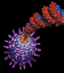
14 Jacques Dubochet Joachim Frank Richard Henderson 2017 Press Release: The Nobel Prize in Chemistry October 2017 The Royal Swedish Academy of Sciences has decided to award the Nobel Prize in Chemistry 2017 to Jacques Dubochet University of Lausanne, Switzerland Joachim Frank Columbia University, New York, USA and Richard Henderson MRC Laboratory of Molecular Biology, Cambridge, UK "for developing cryo-electron microscopy for the high-resolution structure determination of biomolecules in solution"
15 The Nobel Prize in Chemistry 2017 Press release in 1990, Richard Henderson succeeded in using an electron microscope to generate a three-dimensional image of a protein at atomic resolution. This breakthrough proved the technology s potential. Joachim Frank made the technology generally applicable. Between 1975 and 1986 he developed an image processing method in which the electron microscope s fuzzy twodimensional images are analysed and merged to reveal a sharp three-dimensional structure. Jacques Dubochet added water to electron microscopy. Liquid water evaporates in the electron microscope s vacuum, which makes the biomolecules collapse. In the early 1980s, Dubochet succeeded in vitrifying water he cooled water so rapidly that it solidified in its liquid form around a biological sample, allowing the biomolecules to retain their natural shape even in a vacuum.

16 The Nobel Prize in Chemistry

17 The Nobel Prize in Chemistry


18 Chemistry Nobel Prize 2016 for molecular nanomachines Jean-Pierre Sauvage, Sir J Fraser Stoddart and Bernard L Feringa Introduction 18


19 Physics Nobel Prize 2016 for topological phase transitions and topological phases of matter David Thouless, Duncan Haldane and Michael Kosterlitz Introduction 19


20 2016: 30 years of the Nobel Prize for scanning tunnelling microscopy (STM) and the first report of atomic force microscopy (AFM). Introduction 20


21 Nobel Prize for scanning tunnelling microscopy (STM) The Nobel Prize in Physics 1986 was divided, one half awarded to Ernst Ruska "for his fundamental work in electron optics, and for the design of the first electron microscope", the other half jointly to Gerd Binnig and Heinrich Rohrer "for their design of the scanning tunneling microscope". Introduction 21


22 Tunneling effect The Nobel Prize in Physics 1973 Leo Esaki, Ivar Giaever, Brian D. Josephson 1973 Ivar Giaever Prize motivation: "for their experimental discoveries regarding tunnelling phenomena in semiconductors and superconductors, respectively" Field: condensed matter physics, semiconductors Beginning of nanophysics: in 1951, Gorter suggested that experiments by van Itterbeek and coworkers, who measured the current through metal grains embedded in an isolated matrix, could be explained by single-electron charging. Superconductivity in Nanosystems 22


23 Quantum tunneling: Ivar Giaver May 2012, Lofoten Following on Esaki's discovery of electron tunnelling in semiconductors in 1958, Giaever showed that tunnelling also took place in superconductors (1960). Giaever's demonstration of tunnelling in superconductors stimulated Brian Josephson to work on the phenomenon, leading to his prediction of the Josephson effect in Esaki and Giaever shared half of the 1973 Nobel Prize, and Josephson received the other half. Electron phase coherence


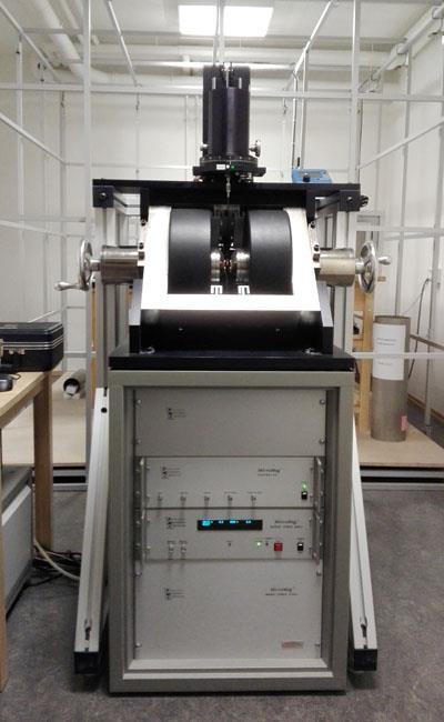
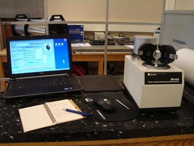
24 Official opening on 7 September 2016 Instruments for Paleomagnetic Measurements and Rock Magnetic Analyses AGICO JR-6A Spinner Magnetometer Lake Shore PMC MicroMag 3900 Vibrating Sample Magnetometer (VSM)

25 2016: Memristor behaves like a synapse Researchers led by Qiangfei Xia and Joshua Yang at the University of Massachusetts at Amherst in the US have made a "diffusive" memristor that emulates how a real synapse works. The device could be used as a key element in integrated circuits and next-generation computers that mimic how the human brain works. The new device is made from a memory resistor or memristor (a resistor that remembers how much current has flowed through it). Unlike other modern-day electronics memories like those made from CMOS devices, memristors are able to remember their state (that is the information stored in them) even if you lose power. They also use much less energy and, importantly, so-called diffusive memristors can realistically mimic how ions, such as Ca 2+, diffuse through synapses. Introduction 25


26 2016: Other highlights Graphene patch detects glucose in sweat Quantum-dot barcodes for diagnosing disease Polymeric nanoparticles deliver anti-inflammatory proteins Nanotube array transistor breaks new record Graphene composite enables metre-sized flexible displays 2D perovskite solar cells break new efficiency record Self-powered textile could be woven into smart clothes t 19. What applications of nanophysics do you know? Nanostructured supercapacitors empower sustainable storage Flexible LG display Samsung Galaxy S8 with 10-nm design Qualcomm Snapdragon 830 microprocessor Lenovo folding display Introduction 26


27 2017 highlights World's Smallest Christmas Card Offers Season's Tiniest Greetings Practical Quantum Computers Self-Driving Trucks Brain implants to restore the freedom of movement Amazing Artificial Intelligence Achievements Samsung: Pushing the boundaries in OLEDs Samsung Galaxy S8 with 10 nm design released 4K and Ultra HD screens: the hot new resolution t 19. What applications of nanophysics do you know? World's Smallest Christmas Card Quantum Computer Introduction 27


28 2017 highlights Graphene composite provides wireless power Designing highly reversible aluminum-ion batteries with graphene Graphene-oxide membranes filter organic solutions Brain-penetrating nanoparticles restore neuron function Nanotechnology takes on microbial drug resistance Nanoparticles resurrect antibacterial drugs High conductance detected in a human integrin protein t 19. What applications of nanophysics do you know? Nano-patterning technique records structural color at low cost Nanomaterials help fight infectious disease Fixed-junction device for protein measurement Nano-cone arrays produce structural color by diffraction. Introduction 28

29 Physicists build muscle for shape-changing, cell-sized robots January 3, 2018 Cornell University Robotics experts have made a robot exoskeleton that can rapidly change its shape upon sensing chemical or thermal changes in its environment. And, they claim, these microscale machines equipped with electronic, photonic and chemical payloads could become a powerful platform for robotics at the size scale of biological microorganisms. Introduction 29


30 What number of electrons can we expect in mesoscopic objects? 1 nm 3 ~ 30 atoms (5 nm) 3 ~ 125 x 30 = 3750 atoms C 6 el./atom Ge 32 el./atom Ga 31 el./atom As 33 el./atom Hund's rules Introduction to Nanophysics 30
31 Electron orbitals and shells in atoms In atoms number of electrons per shell is 2n 2 : 2, 8, 18, 32 In atoms number of electrons per orbit is 2(2l+1): 2,6,10,14,18,22,26 Introduction to Nanophysics 31
32 Role of surface effects in mesoscopic objects t 2. What happens to the laws of physics on a mesoscopic scale? Give an example. A / V = 6a 2 / a 3 = 6 / a = 6 V -1/3 V = a 3 (2a) 3 = 8 a 3 (5a) 3 = 125 a 3 (10a) 3 = 1000 a 3 Percentage of surface atoms : 100% 100% 78,4% 48,8% Macroscopic: V = (10 8 a) 3 = a 3 A = 6 (10 8 a) 2 = a 2 Percentage of surface atoms: %!!! (negligible) Introduction to Nanophysics 32

33 Classical vs. Quantum Physics for mesoscopic objects t 2. What happens to the laws of physics on a mesoscopic scale? Give an example. Classical Mechanics Electrodynamics Thermodynamics Quantum Mechanics Quantum Electrodynamics Quantum Statistics Mesoscopic phenomena (quasiclassical regime) Introduction 33

34 Moor s law and necessity for mesoscopics t 1. What is Moore s law? Why do we need Nanophysics? Introduction 34
 In 2010 chips were based on the design rule of 22 nm.")
35 CMOS TECHNOLOGY complementary metal-oxide semiconductor technology Intel s Norwood (Pentium nm) processor Intel s Prescott processor (released March 2004): 150 million transistors 90 nm design rules 3.4 GHz clock frequency DRAM chips: Dynamic random-access memory 4 Gb chips demonstrated (~ 10 9 transistors/cm 2 ) In 2010 chips were based on the design rule of 22 nm. 20 years back we were already Introduction well inside nanotechnology! 35


36 Progress in miniaturisation By Cmglee - Own work, CC BY-SA 3.0, t 1. What is Moore s law? Why do we need Nanophysics? Introduction 36
37 Main ingredients of nanoelectronics Two-dimensional electron gas (2DEG) Quantum wires and point contacts Quantum dots Nano-electro-mechanical systems Vibrating carbon and non-carbon nanotubes and other molecular devices Devices using superconductivity and magnetism at nanoscale Devices for quantum computation Novel devices Spintronics manipulation of electron spin Introduction 37
 New systems: Carbon nanotubes, etc t 18. What semiconducting materials are usually used in the nano-industry and nanophysics experiments? What are reasons for that?")
38 Samples, materials, and experimental techniques Semiconductor devices: GaAlAs heterostructures (optoelectronics, high mobility under modulation doping) Si-MOSFET (silicon has a natural oxide, that is very important) New systems: Carbon nanotubes, etc t 18. What semiconducting materials are usually used in the nano-industry and nanophysics experiments? What are reasons for that? Structure of a carbon nanotube. The circles denote carbon atoms in a graphite sheet, which is rolled up and forms a tube with a diameter of a few nanometers. The ends are supposedly capped by a carbon hemisphere. Introduction 38
![Materials for nano-industry Ga[Al]As Si 18.](/docs-images/82/85246317/images/39-0.jpg "twhat semiconducting materials are usually used in the nano-industry and")

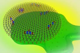
39 Materials for nano-industry Ga[Al]As Si 18. twhat semiconducting materials are usually used in the nano-industry and nanophysics experiments? What are reasons for that? Self-assembled quantum dots are periodic arrays of artificial atoms. They are considered to be promising systems for heterostructure lasers. Introduction 39
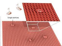
40 SINGLE-ELECTRON SINGLE-MOLECULE TRANSISTORS J. Park et al. (2002) t 18. What semiconducting materials are usually used in the nano-industry and nanophysics experiments? What are reasons for that? see also: - E. S. Soldatov et al. (1996) - H. Park et al. (2000) - N. Zhitenev et al. (2002) - S. Kubatkin et al. (2003) SET within the Orthodox theory: C 1 = C 2 = C/2 R 1 = R 2 = R/2 Current I (e/rc) k B T = 0.01 e 2 /C Q e = e/2 Q e = 0 V t (for Q 0 = 0) Introduction Source-drain Voltage V (e/c) 40


41 Instrumentation for nanoscience and nanotechnology Growth Fabrication Characterization MBE EBL STM Quantum corralls Introduction 41


42 New laws of Nature at nanoscale? In a classical resistor, the resistance is due to electron scattering. Otherwise electrons are just accelerated by the electric field. 2. twhat happens to the laws of physics on a mesoscopic scale? Give an example. QM: Particle or wave? 5. twhat length scale is important for a double slit experiment in the solid state? Please explain. Quantum modes in the wire Electron diffraction is controlled by phase coherence length Introduction 42
43 Classical versus quantum physics t 2. What happens to the laws of physics on a mesoscopic scale? Give an example. Introduction 43
44 Basic problems Features of nanoscale systems: Quantum transport Specific electron-electron interaction, which is more pronounced in low-dimensional systems Stronger role of disorder Enhanced role of contacts and electromagnetic environment Nano-devices are usually out of equilibrium, which requires special understanding t 2. What happens to the laws of physics on a mesoscopic scale? Give an example. All these issues are far from being fully understood It is new research area with rich physics and chemistry! Introduction 44


45 Quantum Mechanics of Interacting Particles Condensation Wigner crystal Introduction 45


46 Self-assembly systems Nanomaterials Encapsulated 4 nm Au particles self-assembled into a 2D array supported by a thin film, Anders et al., 1995 Scheme for molecular manufacturing Introduction 46

47 In nanomaterials electrical and mechanical energies are comparable Electrical and mechanical modes are strongly coupled Nano-electro-mechanics Examples of the systems Electron shuttles Molecular motors Carbon nanotubes Introduction 47

48 Shuttle transfer of electrons A movable cluster conveys electron one by one In some cases electro-mechanic instabilities can take place Shuttle transport has been observed in several concrete systems Introduction 48


 ; Caltech, US; FOM-Institute, AMOLF, the Netherlands.")
49 Solar cells with nanoparticles: Nanoplasmonics Main principle: Plasmon resonances due to nanoparticles strongly enhance the time, which photons spend close to the active layer Metallic nanoparticles embedded in the host system close to the active layer Simulation of increased light intensity beneath a metal nanoparticle on a silicon cell Key players: Centre for Sustainable Energy Systems at the Australian National University (ANU) ; Caltech, US; FOM-Institute, AMOLF, the Netherlands. Introduction 49


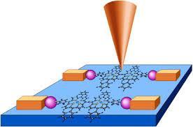
 l Fluks kvantum: B")
50 Mesoscopic Superconductivity Studies of individual magnetic vortices by magneto-optical (MO) imaging Tom Henning Johansen et al., Univ. Oslo x J B(r) l Fluks kvantum: B da = Introduction 50


51 One can take snapshots at different times, and in this way observe vortex dynamics Example: Edge effects prøvekant 10 m MOI single vortices allows to study and influence mesoscopic structure of vortex matter Introduction 51

52 More about physical scales Classical length electron mean free path, Quantum length de Broglie wavelength of an electron having the Fermi energy: t 4. What is de Broglie wavelength of electrons and size quantization? This scale is relevant to the size quantization quantum films, wires, and dots Introduction 52
53 Another important scale phase coherence length, Scale introduced by Coulomb interaction and depending on the device capacitance, C - relevant to single-electron tunneling Interplay between different scales leads to a rich picture of transport through nanosystems. The specific properties of different regimes can be used for various applications. t 6. What is the role of charging effects on nano-scale? Introduction 53
54 Basic classification of transport regimes mean free path phase coherence length Fermi wavelength t 3. What are characteristic length scales and specific parameters that define transition to mesoscopic regime? Introduction 54
55 Two-dimensional Electron Gas (2DEG) Band gap engineering 2DEG is a generic object for new physics Metal-Oxide-Semiconductor (MOS) structures 2DEG is formed at the semiconductor-insulator interface Semiconductor heterostructure 2DEG is formed at the interface between two semiconductors Nobel Prizes 1985, 1998, 2000 It serves as a building block for electronic devices We will come back to these structures later Introduction 55


56 Quantum Wires and Point Contacts Cleaved structures Split-gate structures Point contacts Carbon nanotubes Introduction 56
57 Ballistic transport,, quantum point contact To the left, the surface topography of a GaAs microchip is shown. The picture has been taken with an atomic force microscope. The chip hosts a quantum film about 30 nm below its surface, which is removed underneath the bright lines. A small and short wire of length 140 nm and width 80 nm connects source and drain. The measurement to the right shows the conductance of the wire as a function of the gate voltage. At low temperatures, a conductance quantization in units of 2e 2 /h is visible, which vanishes around 20 K. 7. twhat length scale is important for ballistic transport? How is it influenced by temperature? t 10. What is the quantum point contact (QPC), and at what temperatures and lengths does it usually operate? What length scale is important for QPC? Introduction 57
58 Quantization of conductance vs. gate voltage! Conductance quantum: S New universal unit of resistance h/e 2 8. tdoes a ballistic wire have infinite conductance? Absent in classical theory t 9. What is the quantum of conductance? Where does it appear? What is the value of quantum resistance in Ohm? KOhm Introduction 58
59 The quantum Hall effects and Shubnikov-de Haas oscillations Classical Hall effect Shubnikov-de Haas oscillations and the quantum Hall effect. We look at a measurement of the longitudinal and the Hall resistance (R xx and R yy, respectively), of a two dimensional electron gas, as a function of a magnetic field applied perpendicular to the plane of the quantum film. The experiment has been performed at a temperature of 100 mk. The Hall resistance is quantized in units of h/2e 2. t 11. What is the quantum Hall effect and Shubnikov de Haas oscillations? Are these effects linked? In what systems do they take place? In what units is resistance quantized? What temperatures and magnetic fields are essential for these effects? Introduction 59

60 At low temperatures Phase coherence t 13. What is the Aharonov Bohm effect? What is typical geometry of the device showing this effect? What length scale is important for this effect, and by what kind of scattering is it influenced? Is resistance a local property in this effect? Is high magnetic field and low temperatures necessary for it? The resistance of a small ring with a diameter of about 1 micron (the light gray areas in the inset) as a function of a magnetic field applied perpendicular to the ring plane shows periodic oscillations, known as Aharonov-Bohm oscillations. They indicate that a significant fraction of the electrons traverse the ring phase coherently. Dephasing is caused by inelastic (e-ph, e-e) scattering. Diffusive coherent systems are possible. E-e scattering does not contribute to resistance. Introduction 60

61 Single-electron tunneling and quantum dots The right inset shows again the surface topography of a semiconductor with a two dimensional electron gas underneath. The bright lines enclose a small island. It is coupled to source and drain via two quantum point contacts, forming tunnel barriers for the electrons. The barriers are tuned by adjusting the voltages at the gates Ql and Q2. The main figure shows the conductance through the island as a function of the gate voltage V I applied to region I. V I tunes the potential of the island. The conductance peaks indicate that only for a particular island potential, electrons can be transferred between the island and the leads. The left inset shows a fit to a function one would expect for peaks that are governed by thermal smearing of the Fermi function. t 15. What is a quantum dot and what is its relation to single electron quantum transistor? Introduction 61


62 Quantum Dots Lateral quantum dots Coulomb blockage! Ivar Giæver 15. twhat is a quantum dot and what is its relation to single electron quantum transistor? Vertical Artificial atoms new periodic table In atoms number of electrons per shell is 2n 2 : 2, 8, 18, 32 In artificial atoms number of electrons per shell is : 2, 6, 12, 20 Introduction 62


63 Coulomb blockade Gate Electron Dot t 14. What is single-electron tunneling and the role of capacitance in this effect? What is the characteristic energy that plays a major role in this effect? Cost Repulsion at the dot Attraction to the gate At the energy cost vanishes! Single-electron transistor (SET) Introduction 63
64 Fermi wavelength 21. Why does Fermi wavelength decrease with the electron density? What is the relation between Fermi wavelength and electron density in different dimensions? Can you derive this? Can you find mistakes in TH p. 158 (pdf)? Introduction 64
65 Density of states 12. What is the role of Fermi wavelength in changing the dimensionality of mesoscopic systems? Is it related to de Broglie wavelength? What are the implications of changing dimensionality? What is the density of states as function of energy per unit volume in systems of different dimensions? Can you derive this? Electron density of states in the effective mass approximation as a function of energy, in one, two, and three dimensions Update of solid state physics 65
66 Density of states Two dimensional system, periodic boundary conditions Momentum is quantized in units of A quadratic lattice in k-space, each of them is g-fold degenerate (spin, valleys). Assume that, the limit of continuous spectrum. Number of states between k and k+dk: Update of solid state physics 66


67 Number of states per volume per the region k,k+dk Density of states -Number of states per volume per the region E,E+dE. Since 3 Update of solid state physics 67

68 Electron spin Was first introduced in 1925 by Uhlenbeck and Goudsmit to explain the hyperfine structure of the atomic spectrum. 16. What is the role of electron spin in solid-state physics? What characteristic length scale is important in nanospintronics? Do you know any commercial devices that use spin of electrons? A theoretical foundation has been provided in 1928 by Dirac by making a relativistic correction to the wave equation. Spintronics 68


69 Giant magnetoresistance In GMR, resistance depends on the relative orientation of the electron spin-defined magnetizations of the ferromagnetic layers. 16. What is the role of electron spin in solid-state physics? What characteristic length scale is important in nanospintronics? Do you know any commercial devices that use spin of electrons? Giant magnetoresistance 69


70 Electronics applications 16. What is the role of electron spin in solid-state physics? What characteristic length scale is important in nanospintronics? Do you know any commercial devices that use spin of electrons? t 19. What applications of nanophysics do you know? Spintronics 70
71 Mesoscopic effects: role of temperature The typical length scale at which the mesoscopic regime is reached depends on the temperature. The numbers below give an order of magnitude. Temperature (K) L (nm) 4.2 (liquid helium) < (liquid nitrogen) < (room temperature) < What energies and temperatures are typical for mesoscopic electronic devices? What is the relation between temperature and electron energy? What is typical length scale at which the mesoscopic regime takes place at different temperatures? t 20. What determines the temperature at which a mesoscopic effect vanishes? How is it in contrast with superconductivity? Update of solid state physics 71

72 Quantum scattering length 22. What is quantum scattering length and quantum scattering time? Is it the same as Drude scattering time τ? t 22. What is quantum scattering length and quantum scattering time? Is it the same as Drude scattering time τ? Introduction 72


73 Diffusive transport Between scattering events electrons move like free particles with a given effective mass. In 1D case the relation between the final velocity and the effective free path, l, is then Assuming where is the drift velocity while is the typical velocity and introducing the collision time as we obtain in the linear approximation: Mobility Update of solid state physics 73
74 Dephasing time 23. thow does dephasing time of electrons depend on T at low and high temperatures? τ Introduction 74
Meeting of Modern Science and School Physics: College for School Teachers of Physics in ICTP. 27 April - 3 May, 2011
 2234-7 Meeting of Modern Science and School Physics: College for School Teachers of Physics in ICTP 27 April - 3 May, 2011 Introduction to nanophysics Yuri Galperin University of Oslo Oslo Norway Very
From nanophysics research labs to cell phones. Dr. András Halbritter Department of Physics associate professor
 From nanophysics research labs to cell phones Dr. András Halbritter Department of Physics associate professor Curriculum Vitae Birth: 1976. High-school graduation: 1994. Master degree: 1999. PhD: 2003.
Nanotechnology. Yung Liou P601 Institute of Physics Academia Sinica
 Nanotechnology Yung Liou P601 yung@phys.sinica.edu.tw Institute of Physics Academia Sinica 1 1st week Definition of Nanotechnology The Interagency Subcommittee on Nanoscale Science, Engineering and Technology
Carbon based Nanoscale Electronics
 Carbon based Nanoscale Electronics 09 02 200802 2008 ME class Outline driving force for the carbon nanomaterial electronic properties of fullerene exploration of electronic carbon nanotube gold rush of
Solid Surfaces, Interfaces and Thin Films
 Hans Lüth Solid Surfaces, Interfaces and Thin Films Fifth Edition With 427 Figures.2e Springer Contents 1 Surface and Interface Physics: Its Definition and Importance... 1 Panel I: Ultrahigh Vacuum (UHV)
The Physics of Nanoelectronics
 The Physics of Nanoelectronics Transport and Fluctuation Phenomena at Low Temperatures Tero T. Heikkilä Low Temperature Laboratory, Aalto University, Finland OXFORD UNIVERSITY PRESS Contents List of symbols
Nanoscience, MCC026 2nd quarter, fall Quantum Transport, Lecture 1/2. Tomas Löfwander Applied Quantum Physics Lab
 Nanoscience, MCC026 2nd quarter, fall 2012 Quantum Transport, Lecture 1/2 Tomas Löfwander Applied Quantum Physics Lab Quantum Transport Nanoscience: Quantum transport: control and making of useful things
phys4.20 Page 1 - the ac Josephson effect relates the voltage V across a Junction to the temporal change of the phase difference
 Josephson Effect - the Josephson effect describes tunneling of Cooper pairs through a barrier - a Josephson junction is a contact between two superconductors separated from each other by a thin (< 2 nm)
Minimal Update of Solid State Physics
 Minimal Update of Solid State Physics It is expected that participants are acquainted with basics of solid state physics. Therefore here we will refresh only those aspects, which are absolutely necessary
Building blocks for nanodevices
 Building blocks for nanodevices Two-dimensional electron gas (2DEG) Quantum wires and quantum point contacts Electron phase coherence Single-Electron tunneling devices - Coulomb blockage Quantum dots (introduction)
Mesoscopic Nano-Electro-Mechanics of Shuttle Systems
 * Mesoscopic Nano-Electro-Mechanics of Shuttle Systems Robert Shekhter University of Gothenburg, Sweden Lecture1: Mechanically assisted single-electronics Lecture2: Quantum coherent nano-electro-mechanics
CH676 Physical Chemistry: Principles and Applications. CH676 Physical Chemistry: Principles and Applications
 CH676 Physical Chemistry: Principles and Applications History of Nanotechnology: Time Line Democritus in ancient Greece: concept of atom 1900 : Rutherford : discovery of atomic nucleus The first TEM was
Nanomaterials and their Optical Applications
 Nanomaterials and their Optical Applications Winter Semester 2013 Lecture 02 rachel.grange@uni-jena.de http://www.iap.uni-jena.de/multiphoton Lecture 2: outline 2 Introduction to Nanophotonics Theoretical
Nanoelectronics. Topics
 Nanoelectronics Topics Moore s Law Inorganic nanoelectronic devices Resonant tunneling Quantum dots Single electron transistors Motivation for molecular electronics The review article Overview of Nanoelectronic
Chapter 1 Introduction
 Chapter 1 Introduction A nanometer (nm) is one billionth (10-9 ) of a meter. Nanoscience can be defined as the science of objects and phenomena occurring at the scale of 1 to 100 nm. The range of 1 100
Chapter 3 Properties of Nanostructures
 Chapter 3 Properties of Nanostructures In Chapter 2, the reduction of the extent of a solid in one or more dimensions was shown to lead to a dramatic alteration of the overall behavior of the solids. Generally,
Modern physics. 4. Barriers and wells. Lectures in Physics, summer
 Modern physics 4. Barriers and wells Lectures in Physics, summer 016 1 Outline 4.1. Particle motion in the presence of a potential barrier 4.. Wave functions in the presence of a potential barrier 4.3.
CHAPTER 11 Semiconductor Theory and Devices
 CHAPTER 11 Semiconductor Theory and Devices 11.1 Band Theory of Solids 11.2 Semiconductor Theory 11.3 Semiconductor Devices 11.4 Nanotechnology It is evident that many years of research by a great many
From Last Time. Partially full bands = metal Bands completely full or empty = insulator / seminconductor
 From Last Time Solids are large numbers of atoms arranged in a regular crystal structure. Each atom has electron quantum states, but interactions shift the energies. End result is each type atomic electron
Condensed Matter Physics: From Stone Age Pottery to Topological Quantum Computing
 Condensed Matter Physics: From Stone Age Pottery to Topological Quantum Computing Hanno Weitering Department of Physics and Astronomy The Joint Institute for Advanced Materials A physicist s view of the
Spintronics. Seminar report SUBMITTED TO: SUBMITTED BY:
 A Seminar report On Spintronics Submitted in partial fulfillment of the requirement for the award of degree of Electronics SUBMITTED TO: SUBMITTED BY: www.studymafia.org www.studymafia.org Preface I have
Nanophysics: Main trends
 Nano-opto-electronics Nanophysics: Main trends Nanomechanics Main issues Light interaction with small structures Molecules Nanoparticles (semiconductor and metallic) Microparticles Photonic crystals Nanoplasmonics
News from NBIA. Condensed Matter Physics: from new materials to quantum technology. time. Mark Rudner
 News from NBIA Condensed Matter Physics: from new materials to quantum technology Mark Rudner time ~100 years after Bohr, the basic laws and players are established 1913 2013 Image from www.periodni.com
Solid State Physics (Major, 8 ECTS)
") Solid State Physics (Major, 8 ECTS) 1 physicist over 3 in US declares to be a condensed matter physicist (CMP) CMP: solids, amorphous materials, liquids, soft materials 20 CMP physics Nobel prizes + 5
Solid State Physics (Major, 8 ECTS) 1 physicist over 3 in US declares to be a condensed matter physicist (CMP) CMP: solids, amorphous materials, liquids, soft materials 20 CMP physics Nobel prizes + 5
What is Quantum Transport?
 What is Quantum Transport? Branislav K. Nikolić Department of Physics and Astronomy, University of Delaware, U.S.A. http://www.physics.udel.edu/~bnikolic Semiclassical Transport (is boring!) Bloch-Boltzmann
PHYS 3313 Section 001 Lecture #21 Monday, Nov. 26, 2012
 PHYS 3313 Section 001 Lecture #21 Monday, Nov. 26, 2012 Superconductivity Theory, The Cooper Pair Application of Superconductivity Semi-Conductor Nano-technology Graphene 1 Announcements Your presentations
Impact of disorder and topology in two dimensional systems at low carrier densities
 Impact of disorder and topology in two dimensional systems at low carrier densities A Thesis Submitted For the Degree of Doctor of Philosophy in the Faculty of Science by Mohammed Ali Aamir Department
Information processing in nanoscale systems
 Information processing in nanoscale systems Mark Rudner Niels Bohr International Academy Image from: www.upscale.utoronto.ca 100 years after Bohr, the basic laws and players are established 1913 2013 Image
Classification of Solids
 Classification of Solids Classification by conductivity, which is related to the band structure: (Filled bands are shown dark; D(E) = Density of states) Class Electron Density Density of States D(E) Examples
Overview. Carbon in all its forms. Background & Discovery Fabrication. Important properties. Summary & References. Overview of current research
 Graphene Prepared for Solid State Physics II Pr Dagotto Spring 2009 Laurene Tetard 03/23/09 Overview Carbon in all its forms Background & Discovery Fabrication Important properties Overview of current
SYLLABUS FINDING NANO Syllabus NanoSCI DISCOVERING NANOTECHNOLOGY AND CULTURE IN GERMANY
 1. Syllabus NanoSCI Course title: NanoSCI - Electronic Properties of Nanoengineered Materials Catalog description: Physics and technology of nanoengineered materials and devices. Semiconductor nanostructures.
Surfaces, Interfaces, and Layered Devices
 Surfaces, Interfaces, and Layered Devices Building blocks for nanodevices! W. Pauli: God made solids, but surfaces were the work of Devil. Surfaces and Interfaces 1 Role of surface effects in mesoscopic
Mesoscopic Nano-Electro-Mechanics of Shuttle Systems
 * Mesoscopic Nano-Electro-Mechanics of Shuttle Systems Robert Shekhter University of Gothenburg, Sweden Lecture1: Mechanically assisted single-electronics Lecture2: Quantum coherent nano-electro-mechanics
Electronic and Optoelectronic Properties of Semiconductor Structures
 Electronic and Optoelectronic Properties of Semiconductor Structures Jasprit Singh University of Michigan, Ann Arbor CAMBRIDGE UNIVERSITY PRESS CONTENTS PREFACE INTRODUCTION xiii xiv 1.1 SURVEY OF ADVANCES
RAJASTHAN TECHNICAL UNIVERSITY, KOTA
 RAJASTHAN TECHNICAL UNIVERSITY, KOTA (Electronics & Communication) Submitted By: LAKSHIKA SOMANI E&C II yr, IV sem. Session: 2007-08 Department of Electronics & Communication Geetanjali Institute of Technical
Lectures: Condensed Matter II 1 Electronic Transport in Quantum dots 2 Kondo effect: Intro/theory. 3 Kondo effect in nanostructures
 Lectures: Condensed Matter II 1 Electronic Transport in Quantum dots 2 Kondo effect: Intro/theory. 3 Kondo effect in nanostructures Luis Dias UT/ORNL Lectures: Condensed Matter II 1 Electronic Transport
single-electron electron tunneling (SET)
") single-electron electron tunneling (SET) classical dots (SET islands): level spacing is NOT important; only the charging energy (=classical effect, many electrons on the island) quantum dots: : level spacing
single-electron electron tunneling (SET) classical dots (SET islands): level spacing is NOT important; only the charging energy (=classical effect, many electrons on the island) quantum dots: : level spacing
Challenges for Materials to Support Emerging Research Devices
 Challenges for Materials to Support Emerging Research Devices C. Michael Garner*, James Hutchby +, George Bourianoff*, and Victor Zhirnov + *Intel Corporation Santa Clara, CA + Semiconductor Research Corporation
There s plenty of room at the bottom! - R.P. Feynman, Nanostructure: a piece of material with at least one dimension less than 100 nm in extent.
 Nanostructures and Nanotechnology There s plenty of room at the bottom! - R.P. Feynman, 1959 Materials behave differently when structured at the nm scale than they do in bulk. Technologies now exist that
1. Introduction : 1.2 New properties:
 Nanodevices In Electronics Rakesh Kasaraneni(PID : 4672248) Department of Electrical Engineering EEL 5425 Introduction to Nanotechnology Florida International University Abstract : This paper describes
QUANTUM- CLASSICAL ANALOGIES
 D. Dragoman M. Dragoman QUANTUM- CLASSICAL ANALOGIES With 78 Figures ^Ü Springer 1 Introduction 1 2 Analogies Between Ballistic Electrons and Electromagnetic Waves 9 2.1 Analog Parameters for Ballistic
Chapter 10. Nanometrology. Oxford University Press All rights reserved.
 Chapter 10 Nanometrology Oxford University Press 2013. All rights reserved. 1 Introduction Nanometrology is the science of measurement at the nanoscale level. Figure illustrates where nanoscale stands
VALLIAMMAI ENGINEERING COLLEGE
 VALLIAMMAI ENGINEERING COLLEGE SRM Nagar, Kattankulathur 603 203 DEPARTMENT OF PHYSICS QUESTION BANK II SEMESTER PH8252 - PHYSICS FOR INFORMATION SCIENCE (Common to CSE & IT) Regulation 2017 Academic Year
Introduction to Scanning Probe Microscopy Zhe Fei
 Introduction to Scanning Probe Microscopy Zhe Fei Phys 590B, Apr. 2019 1 Outline Part 1 SPM Overview Part 2 Scanning tunneling microscopy Part 3 Atomic force microscopy Part 4 Electric & Magnetic force
Electronic Quantum Transport in Mesoscopic Semiconductor Structures
 Thomas Ihn Electronic Quantum Transport in Mesoscopic Semiconductor Structures With 90 Illustrations, S in Full Color Springer Contents Part I Introduction to Electron Transport l Electrical conductance
Nanoscale Energy Transport and Conversion A Parallel Treatment of Electrons, Molecules, Phonons, and Photons
 Nanoscale Energy Transport and Conversion A Parallel Treatment of Electrons, Molecules, Phonons, and Photons Gang Chen Massachusetts Institute of Technology OXFORD UNIVERSITY PRESS 2005 Contents Foreword,
Lecture 20: Semiconductor Structures Kittel Ch 17, p , extra material in the class notes
 Lecture 20: Semiconductor Structures Kittel Ch 17, p 494-503, 507-511 + extra material in the class notes MOS Structure Layer Structure metal Oxide insulator Semiconductor Semiconductor Large-gap Semiconductor
Understanding the properties and behavior of groups of interacting atoms more than simple molecules
 Condensed Matter Physics Scratching the Surface Understanding the properties and behavior of groups of interacting atoms more than simple molecules Solids and fluids in ordinary and exotic states low energy
Electrical and Optical Properties. H.Hofmann
 Introduction to Nanomaterials Electrical and Optical Properties H.Hofmann Electrical Properties Ohm: G= σw/l where is the length of the conductor, measured in meters [m], A is the cross-section area of
 http://www.physics.ucdavis.edu/condensed_matter.html A brief introduction to Condensed Matter Physics at Davis and an overview of the Condensed Matter Experiment Group The Past-- 30 Years of Nobel Prizes
1.0 Introduction to Quantum Systems for Information Technology 1.1 Motivation
 QSIT09.V01 Page 1 1.0 Introduction to Quantum Systems for Information Technology 1.1 Motivation What is quantum mechanics good for? traditional historical perspective: beginning of 20th century: classical
Semiclassical formulation
 The story so far: Transport coefficients relate current densities and electric fields (currents and voltages). Can define differential transport coefficients + mobility. Drude picture: treat electrons
Physics of Semiconductors
 Physics of Semiconductors 13 th 2016.7.11 Shingo Katsumoto Department of Physics and Institute for Solid State Physics University of Tokyo Outline today Laughlin s justification Spintronics Two current
Nanoelectronics 08. Atsufumi Hirohata Department of Electronics. Quick Review over the Last Lecture E = 2m 0 a 2 ξ 2.
 Nanoelectronics 08 Atsufumi Hirohata Department of Electronics 09:00 Tuesday, 6/February/2018 (P/T 005) Quick Review over the Last Lecture 1D quantum well : E = 2 2m 0 a 2 ξ 2 ( Discrete states ) Quantum
Superconductivity at nanoscale
 Superconductivity at nanoscale Superconductivity is the result of the formation of a quantum condensate of paired electrons (Cooper pairs). In small particles, the allowed energy levels are quantized and
Introduction to semiconductor nanostructures. Peter Kratzer Modern Concepts in Theoretical Physics: Part II Lecture Notes
 Introduction to semiconductor nanostructures Peter Kratzer Modern Concepts in Theoretical Physics: Part II Lecture Notes What is a semiconductor? The Fermi level (chemical potential of the electrons) falls
Seminars in Nanosystems - I
 Seminars in Nanosystems - I Winter Semester 2011/2012 Dr. Emanuela Margapoti Emanuela.Margapoti@wsi.tum.de Dr. Gregor Koblmüller Gregor.Koblmueller@wsi.tum.de Seminar Room at ZNN 1 floor Topics of the
Superconductivity at nanoscale
 Superconductivity at nanoscale Superconductivity is the result of the formation of a quantum condensate of paired electrons (Cooper pairs). In small particles, the allowed energy levels are quantized and
Current and Resistance
 Chapter 26 Current and Resistance Copyright 26-1 Electric Current As Fig. (a) reminds us, any isolated conducting loop regardless of whether it has an excess charge is all at the same potential. No electric
Scanning gate microscopy and individual control of edge-state transmission through a quantum point contact
 Scanning gate microscopy and individual control of edge-state transmission through a quantum point contact Stefan Heun NEST, CNR-INFM and Scuola Normale Superiore, Pisa, Italy Coworkers NEST, Pisa, Italy:
Quantum Phenomena & Nanotechnology (4B5)
") Quantum Phenomena & Nanotechnology (4B5) The 2-dimensional electron gas (2DEG), Resonant Tunneling diodes, Hot electron transistors Lecture 11 In this lecture, we are going to look at 2-dimensional electron
Quantum Phenomena & Nanotechnology (4B5) The 2-dimensional electron gas (2DEG), Resonant Tunneling diodes, Hot electron transistors Lecture 11 In this lecture, we are going to look at 2-dimensional electron
quantum mechanics is a hugely successful theory... QSIT08.V01 Page 1
 1.0 Introduction to Quantum Systems for Information Technology 1.1 Motivation What is quantum mechanics good for? traditional historical perspective: beginning of 20th century: classical physics fails
Nanotechnology where size matters
 Nanotechnology where size matters J Emyr Macdonald Overview Ways of seeing very small things What is nanotechnology and why is it important? Building nanostructures What we can do with nanotechnology?
Lecture 3: Heterostructures, Quasielectric Fields, and Quantum Structures
 Lecture 3: Heterostructures, Quasielectric Fields, and Quantum Structures MSE 6001, Semiconductor Materials Lectures Fall 2006 3 Semiconductor Heterostructures A semiconductor crystal made out of more
2D Materials Research Activities at the NEST lab in Pisa, Italy. Stefan Heun NEST, Istituto Nanoscienze-CNR and Scuola Normale Superiore, Pisa, Italy
 2D Materials Research Activities at the NEST lab in Pisa, Italy Stefan Heun NEST, Istituto Nanoscienze-CNR and Scuola Normale Superiore, Pisa, Italy 2D Materials Research Activities at the NEST lab in
Physics and Material Science of Semiconductor Nanostructures
 Physics and Material Science of Semiconductor Nanostructures PHYS 570P Prof. Oana Malis Email: omalis@purdue.edu Course website: http://www.physics.purdue.edu/academic_programs/courses/phys570p/ 1 Course
Nobel Prize in Physiology or Medicine 2017
 Nobel Prize in Physiology or Medicine 2017 Left to right: Michael Rosbash, Michael W. Young and Jeffrey C. Hall, have been awarded the Nobel Prize in Physiology/ Medicine, 2017. Who has won the Nobel Prize
The phases of matter familiar for us from everyday life are: solid, liquid, gas and plasma (e.f. flames of fire). There are, however, many other
. There are, however, many other") 1 The phases of matter familiar for us from everyday life are: solid, liquid, gas and plasma (e.f. flames of fire). There are, however, many other phases of matter that have been experimentally observed,
1 The phases of matter familiar for us from everyday life are: solid, liquid, gas and plasma (e.f. flames of fire). There are, however, many other phases of matter that have been experimentally observed,
Single Electron Transistor (SET)
") Single Electron Transistor (SET) SET: e - e - dot A single electron transistor is similar to a normal transistor (below), except 1) the channel is replaced by a small dot. C g 2) the dot is separated from
Single Electron Transistor (SET) SET: e - e - dot A single electron transistor is similar to a normal transistor (below), except 1) the channel is replaced by a small dot. C g 2) the dot is separated from
Graphene. Tianyu Ye November 30th, 2011
 Graphene Tianyu Ye November 30th, 2011 Outline What is graphene? How to make graphene? (Exfoliation, Epitaxial, CVD) Is it graphene? (Identification methods) Transport properties; Other properties; Applications;
Index. Index. More information. in this web service Cambridge University Press
 absorption edge, 290 absorption of one photon, 285 acceptors, 118 active medium, 287 active region, 293 alkanethiol endgroups, 150 alligator clips, 147 alloy, 68 amino acids, 145 amorphous, 68 amphoteric,
Ecole Franco-Roumaine : Magnétisme des systèmes nanoscopiques et structures hybrides - Brasov, Modern Analytical Microscopic Tools
 1. Introduction Solid Surfaces Analysis Group, Institute of Physics, Chemnitz University of Technology, Germany 2. Limitations of Conventional Optical Microscopy 3. Electron Microscopies Transmission Electron
Quantum Confinement in Graphene
 Quantum Confinement in Graphene from quasi-localization to chaotic billards MMM dominikus kölbl 13.10.08 1 / 27 Outline some facts about graphene quasibound states in graphene numerical calculation of
Physics Curriculum Map - Norwell High School SUBJECT: Physics Grade Level: 11 or 12. Month or Unit: September
 SUBJECT: Physics Grade Level: 11 or 12 Month or Unit: September Scientific Inquiry Skills Scientific literacy can be achieved as students inquire about chemical phenomena. The curriculum should include
Scanning Probe Microscopy (SPM)
") http://ww2.sljus.lu.se/staff/rainer/spm.htm Scanning Probe Microscopy (FYST42 / FAFN30) Scanning Probe Microscopy (SPM) overview & general principles March 23 th, 2018 Jan Knudsen, room K522, jan.knudsen@sljus.lu.se
http://ww2.sljus.lu.se/staff/rainer/spm.htm Scanning Probe Microscopy (FYST42 / FAFN30) Scanning Probe Microscopy (SPM) overview & general principles March 23 th, 2018 Jan Knudsen, room K522, jan.knudsen@sljus.lu.se
Fundamental concepts of spintronics
 Fundamental concepts of spintronics Jaroslav Fabian Institute for Theoretical Physics University of Regensburg Stara Lesna, 24. 8. 2008 SFB 689 :outline: what is spintronics? spin injection spin-orbit
Introduction to Quantum Dynamics and Control
 EE 290O. Advanced Topics in Control: Introduction to Quantum Dynamics and Control Instructor: Alireza Shabani Contact : shabani@berkeley.edu Office: Gilman, Room 19 Cory 278 Office Hours: Wednesdays 3-4
IH2654 Nanoelectronics, 9hp autumn 2012, period 1 and ****** Nanoelectronics, PhD course
 IH2654 Nanoelectronics, 9hp autumn 2012, period 1 and ****** Nanoelectronics, PhD course For Master programs in Nanotechnology and E, F, ME and PhD students (Previously: 2B1234, 6p and 4H1716, 4p) https://www.kth.se/social/course/ih2654/
6.763 Applied Superconductivity Lecture 1
 6.763 Applied Superconductivity Lecture 1 Terry P. Orlando Dept. of Electrical Engineering MIT September 4, 2003 Outline What is a Superconductor? Discovery of Superconductivity Meissner Effect Type I
EN2912C: Future Directions in Computing Lecture 08: Overview of Near-Term Emerging Computing Technologies
 EN2912C: Future Directions in Computing Lecture 08: Overview of Near-Term Emerging Computing Technologies Prof. Sherief Reda Division of Engineering Brown University Fall 2008 1 Near-term emerging computing
Quantum dots. Quantum computing. What is QD. Invention QD TV. Complex. Lego. https://www.youtube.com/watch?v=ne819ppca5o
 Intel's New 49-qubit Quantum Chip & Neuromorphic Chip https://www.youtube.com/watch?v=ne819ppca5o How To Make a Quantum Bit https://www.youtube.com/watch?v=znzzggr2mhk Quantum computing https://www.youtube.com/watch?v=dxaxptlhqqq
Techniques for inferring M at small scales
 Magnetism and small scales We ve seen that ferromagnetic materials can be very complicated even in bulk specimens (e.g. crystallographic anisotropies, shape anisotropies, local field effects, domains).
Nanostructures. Lecture 13 OUTLINE
 Nanostructures MTX9100 Nanomaterials Lecture 13 OUTLINE -What is quantum confinement? - How can zero-dimensional materials be used? -What are one dimensional structures? -Why does graphene attract so much
Nano-mechatronics. Presented by: György BudaváriSzabó (X0LY4M)
") Nano-mechatronics Presented by: György BudaváriSzabó (X0LY4M) Nano-mechatronics Nano-mechatronics is currently used in broader spectra, ranging from basic applications in robotics, actuators, sensors,
Nano-mechatronics Presented by: György BudaváriSzabó (X0LY4M) Nano-mechatronics Nano-mechatronics is currently used in broader spectra, ranging from basic applications in robotics, actuators, sensors,
From Last Time Important new Quantum Mechanical Concepts. Atoms and Molecules. Today. Symmetry. Simple molecules.
 Today From Last Time Important new Quantum Mechanical Concepts Indistinguishability: Symmetries of the wavefunction: Symmetric and Antisymmetric Pauli exclusion principle: only one fermion per state Spin
Plasmonics. The long wavelength of light ( μm) creates a problem for extending optoelectronics into the nanometer regime.
 creates a problem for extending optoelectronics into the nanometer regime.") Plasmonics The long wavelength of light ( μm) creates a problem for extending optoelectronics into the nanometer regime. A possible way out is the conversion of light into plasmons. They have much shorter
Plasmonics The long wavelength of light ( μm) creates a problem for extending optoelectronics into the nanometer regime. A possible way out is the conversion of light into plasmons. They have much shorter
FUNDAMENTALS OF PHYSICS Vol. II - Quantum Phenpmena In Low-Dimensional Systems- Michael R. Geller QUANTUM PHENOMENA IN LOW-DIMENSIONAL SYSTEMS
 QUANTUM PHENOMENA IN LOW-DIMENSIONAL SYSTEMS Michael R. Geller Department of Physics and Astronomy, University of Georgia, USA Keywords: Aharonov-Bohm effect, Bucky balls, composite fermions, coulomb blockade,
PHYS 3313 Section 001 Lecture #24 Monday, Apr. 21, 2014
 PHYS 3313 Section 001 Lecture #24 Monday, Apr. 21, 2014 Liquid Helium Superconductivity Theory, The Cooper Pair Application of Superconductivity Nano-technology Graphene 1 Announcements Reminder Homework
QUANTUM INTERFERENCE IN SEMICONDUCTOR RINGS
 QUANTUM INTERFERENCE IN SEMICONDUCTOR RINGS PhD theses Orsolya Kálmán Supervisors: Dr. Mihály Benedict Dr. Péter Földi University of Szeged Faculty of Science and Informatics Doctoral School in Physics
GaN based transistors
 GaN based transistors S FP FP dielectric G SiO 2 Al x Ga 1-x N barrier i-gan Buffer i-sic D Transistors "The Transistor was probably the most important invention of the 20th Century The American Institute
Single ion implantation for nanoelectronics and the application to biological systems. Iwao Ohdomari Waseda University Tokyo, Japan
 Single ion implantation for nanoelectronics and the application to biological systems Iwao Ohdomari Waseda University Tokyo, Japan Contents 1.History of single ion implantation (SII) 2.Novel applications
The Dielectric Function of a Metal ( Jellium )
") The Dielectric Function of a Metal ( Jellium ) Total reflection Plasma frequency p (10 15 Hz range) Why are Metals Shiny? An electric field cannot exist inside a metal, because metal electrons follow the
The Dielectric Function of a Metal ( Jellium ) Total reflection Plasma frequency p (10 15 Hz range) Why are Metals Shiny? An electric field cannot exist inside a metal, because metal electrons follow the
Superconductivity. S2634: Physique de la matière condensée & nano-objets. Miguel Anía Asenjo Alexandre Le Boité Christine Lingblom
 Superconductivity S2634: Physique de la matière condensée & nano-objets Miguel Anía Asenjo Alexandre Le Boité Christine Lingblom 1 What is superconductivity? 2 Superconductivity Superconductivity generally
Engineering Physics-II. Question Bank
 Engineering Physics-II Question Bank Unit No I Short Answer Type 1. What are de-broglie waves? 2. Discuss few properties of matter waves. 3. What do you mean by phase velocity and group velocity? 4. What
Nanotechnology Fabrication Methods.
 Nanotechnology Fabrication Methods. 10 / 05 / 2016 1 Summary: 1.Introduction to Nanotechnology:...3 2.Nanotechnology Fabrication Methods:...5 2.1.Top-down Methods:...7 2.2.Bottom-up Methods:...16 3.Conclusions:...19
Experimental Quantum Computing: A technology overview
 Experimental Quantum Computing: A technology overview Dr. Suzanne Gildert Condensed Matter Physics Research (Quantum Devices Group) University of Birmingham, UK 15/02/10 Models of quantum computation Implementations
Lecture 4 Scanning Probe Microscopy (SPM)
") Lecture 4 Scanning Probe Microscopy (SPM) General components of SPM; Tip --- the probe; Cantilever --- the indicator of the tip; Tip-sample interaction --- the feedback system; Scanner --- piezoelectric
Lecture 4 Scanning Probe Microscopy (SPM) General components of SPM; Tip --- the probe; Cantilever --- the indicator of the tip; Tip-sample interaction --- the feedback system; Scanner --- piezoelectric
SYLLABUS ELEC 261: ELECTRONIC MATERIALS AND QUANTUM DEVICES SUMMER 2018
 SYLLABUS ELEC 261: ELECTRONIC MATERIALS AND QUANTUM DEVICES SUMMER 2018 Credit Hours: 3 Time and Place: Online Course Summer Session II: May 29 June 29, 2018 Instructors: Junichiro Kono, Professor of Electrical
Lecture 11 - Phonons II - Thermal Prop. Continued
 Phonons II - hermal Properties - Continued (Kittel Ch. 5) Low High Outline Anharmonicity Crucial for hermal expansion other changes with pressure temperature Gruneisen Constant hermal Heat ransport Phonon
Introduction to Nanotechnology Chapter 5 Carbon Nanostructures Lecture 1
 Introduction to Nanotechnology Chapter 5 Carbon Nanostructures Lecture 1 ChiiDong Chen Institute of Physics, Academia Sinica chiidong@phys.sinica.edu.tw 02 27896766 Carbon contains 6 electrons: (1s) 2,