Semiconductor Quantum Dots
|
|
|
- Marylou Poole
- 6 years ago
- Views:
Transcription

1 Semiconductor Quantum Dots M. Hallermann Semiconductor Physics and Nanoscience St. Petersburg JASS 2005
2 Outline Introduction Fabrication Experiments Applications Porous Silicon II-VI Quantum Dots III-V Quantum Dots Cleaved Edge Overgrowth (CEO) Self Assembling Quantum Dots Electronic Structure
3 Introduction Low Dimensional Systems Motion of electron in conduction band is described by the effective mass concept E Dispersion relation with = 2 p 2 m* ( ) E k 2 2 k = 2 m* In low dimensional systems the carrier motion is quantized in one or more spatial directions p = k
4 Inroduction Density of States 3D Wave function in 3D box of volume 1 Φ lmn ( R) = exp Ω ( ikir) Density of states / per unit volume N 2Ω 4 K Density of states in Energy Ω = LLL x y z 2π l 2πm 2πn =,, Lx Ly L z 3 3 ( K) = K π n3 D ( K) = K 2 ( 2π ) 3 3π 3D 3 d 1 2 m* D ( E) = n ( K) = E E de 2π 3D 3D 2 2 g 3 2 1


 m* =")
5 Introduction Density of States 2D For example ( ) GaAs / Al Ga 0.4 x 1 xas x < quantum well Density of states D ( E) m* = π 2D 2


 = 2 m* 1 2π")
6 Introduction Density of States 1D Quantum wire through cleaved edge overgrowth Density of states D 1D ( E) = 2 m* 1 2π E E nm
7 Introduction Density of States 0D Kinetic quantization along x, y and z-direction Energy spectrum fully quantized Density of States 0D ( ) D E = discrete

 ~ 1/r Tunable Atom Tunable")
8 Introduction Quantum Dots as Artificial Atoms Atom QD QD Particle: Electron Exciton Energy scale: 13eV 100keV Typ. 1 ev Length scale: nm Typ. 10 nm Potential: V(r) ~ 1/r Tunable Atom Tunable properties in QDs
9 Introduction Interest in Quantum Dots Applications Lasers in visible and near infrared spectrum Optical data storage Optical detectors Quantum information processing and cryptography Publications
10 Introduction Requirements for Applications Size E > 3kBT 75meV Crystal quality Uniformity Density Growth compatibility Confinement for electrons and/or holes Electrically active matrix material
11 Outline Introduction Fabrication Experiments Applications Porous Silicon II-VI Quantum Dots III-V Quantum Dots Cleaved Edge Overgrowth (CEO) Self Assembling Quantum Dots Electronic Structure


12 Fabrication Experiments Applications Introduction Several approaches: Porous Silicon Nanometer semiconductor inclusions in matrices Lithographic patterning of higher dimensional systems Strain driven selfassembly
13 Outline Introduction Fabrication Experiments Applications Porous Silicon II-VI Quantum Dots III-V Quantum Dots Cleaved Edge Overgrowth (CEO) Self Assembling Quantum Dots Electronic Structure
14 Porous Silicon Introduction C-Si: indirect bandgap inefficient emitter even at 4K P-Si: emission efficiency up to 10% (optical excitation) Nanocrystals of different size and shape Structure of high complexity Confinement leads to bandgap widening and higher overlap of wavefunctions Light emission: surface core nanocrystal Easy fabrication of p-si Pure Si optoelectronic devices possible


15 Porous Silicon Fabrication Anodic biased c-si in hydrofluoric acid (HF) Structure depends on: Doping Etching conditions Illumination conditions
16 Porous Silicon Optical Properties PL Intensity (arb.units) 1 0 Si bandgap Smaller nc s size Widely tunable emission band due to quantum size effect: all emission energies are available 1,0 1,2 1,4 1,6 1,8 2,0 2,2 2,4 Energie [ev] Broad spectrum line narrowing
17 Porous Silicon k-space PL Intensity (arb. units) TO+O(Γ) x5 TO Energy (ev) TA x10 Free exciton P-Si has indirect nature k-conservation rule breaks down due to confinement PL Intensity (arb. units) TO TO+TA TO TA 2 TA E ex. 1,3 1,4 1,5 2 TO Energy (ev) TO+TA TO TA E ex. 1,2 1,3 1,4
18 Porous Silicon Electron-Hole Exchange Interaction PL Intensity (arb. units) 1 T=1.5 K PL Intensity (arb. units) Energy (ev) Energy (ev) Laser Absorption in a singlet state After spin flip emission via triplet state Electronic structure of excitons is very similar to dye molecules
19 Porous Silicon Indirect Excitation: Photosensitization Basic principle: S 1 hν S 0 T 0 Donor Energy Transfer R S T Acceptor Energy transfer (dipole-dipole or direct electron exchange) is efficient if: photoexcited donor has long lifetime overlap of energy bands of D/A is good space separation of D/A is small Silicon nanocrystals (almost ideal donor): ground state is triplet long exciton lifetime ( s) wide emission band huge internal surface area (10 3 m 2 /cm 3 ) Acceptor having triplet ground state?
20 1.63 ev 0.98 ev Porous Silicon Molecular Oxygen: Electronic Structure 1 Σ 1 3 Σ O O ground gtate: spin triplet chemically inert (reaction S+T S is forbidden) excited states: spin singlet energy-rich high chemical reactivity (reaction S+S S is allowed oxidation reactions in organic chemistry, biology, life science photodynamic cancer therapy oxygen-iodine laser Optical excitation is impossible Photosensitizer is required Silicon nanocrystals
21 Porous Silicon PL Quenching by Oxygen Molecules Σ 10-2 mbar O 2 T=5K PL Intensity (arb. units) Σ Energy (ev) Adsorption of O 2 : PL Quenching low temperature: fine structure appears 1 D 3 S emission line of O 2
22 Outline Introduction Fabrication Experiments Applications Porous Silicon II-VI Quantum Dots III-V Quantum Dots Cleaved Edge Overgrowth (CEO) Self Assembling Quantum Dots Electronic Structure

23 II-VI Quantum Dots Introduction First hints of quantum dots: CdSe and CdS in silicate glasses (X-ray 1932) Since 1960s semiconductor doped glasses used as sharp-cut color filter Quantum dots in glassy matrices Ideal model for the study of basic concepts of 3D confinement in semiconductors Many different matrices: glasses, solutions, polymers, even cavities of zeoliths Many promising applications already on the way

24 II-VI Quantum Dots Growth of Nanocrystals Colloidal QDs can be further processed and incorporated in a variety of media CdSe can be prepared in a wide range of shapes
ZnS")
ZnS in PLMA for temperature measurements CdSe in")
25 II-VI Quantum Dots Growth of Nanocrystals In polymer composites Nearly full color emitting LEDs (CdSe)ZnS in PLMA (green red) (CdS)ZnS in PLMA (violet blue) (CdS)ZnS in PLMA for temperature measurements CdSe in TOPO

26 II-VI Quantum Dots Applications Coupled to bio-molecules biological sensors
27 II-VI Quantum Dots Bandstructure Type-I core-shell structure (CdSe)CdS Display devices and lasers CdS CdSe Potential e Type-II (CdTe)CdSe and (CdSe)ZnTe h R CdS CdSe CdS Esp. photovoltaic photoconducting devices Energies smaller than bandgap of each material possible Tunable bandgap low yield (<5%)
28 Outline Introduction Fabrication Experiments Applications Porous Silicon II-VI Quantum Dots III-V Quantum Dots Cleaved Edge Overgrowth (CEO) Self Assembling Quantum Dots Electronic Structure
29 CEO Molecular-Beam-Epitaxy (MBE) Quantum Well E c t D(E) E 1 E c E 0 MBE Atomically precise deposition of layers with different composition and/or doping 2D E


30 CEO Process cleave the sample
31 CEO Process

32 CEO QDs via 2x CEO
33 CEO Lateral Aligned Quantum Dots 1 st : grow AlAs layers in GaAs matrix 2 nd : cleave in MBE machine 2nd growth [110] 3 rd : grow InAs Dots on MBE patterned (110) surface [001] 1st growth
34 CEO Atomic Force Microscopy I [001] SL1 [110] SL4 1µm SL2 SL3
![CEO Atomic Force Microscopy II [110] [001] SL1 SL 2 SL3 SL4](/docs-images/76/73169687/images/35-2.jpg "AlAs-width [nm] 32 20 11 20 dot width [nm] 35 22 12 22 dot height")
![[nm] 13 ±4 7 ±1 3 7 ±1 1µm density [dots/µm] 17 14 ----- ----- SL 1](/docs-images/76/73169687/images/35-3.jpg "2 3 4 quantum dot size correlated with AlAs-width create")
35 CEO Atomic Force Microscopy II [110] [001] SL1 SL 2 SL3 SL4 AlAs-width [nm] dot width [nm] dot height [nm] 13 ±4 7 ±1 3 7 ±1 1µm density [dots/µm] SL quantum dot size correlated with AlAs-width create chessboard-structure?
36 Fabrication Methods CEO Conclusions Advantages Very high crystal quality Confinement for both electrons and holes Flexibility Disadvantages Relatively low confinement energies ( ~10meV) Complex crystal growth and fabrication (011) surface not purely As or Ga terminated like (100)
37 Outline Introduction Fabrication Experiments Applications Porous Silicon II-VI Quantum Dots III-V Quantum Dots Cleaved Edge Overgrowth (CEO) Self Assembling Quantum Dots Electronic Structure
38 Self Assembling QDs Epitaxial Growth Modes


39 Self Assembling QDs Energy Gap vs. Lattice Constant

40 Self Assembling QDs Strained Layer Epitaxy

41 Self Assembling QDs Growth Modes in Strained Systems

42 Self Assembling QDs Stranski-Krastanov Growth Nanostructures formed during lattice mismatched epitaxy (e.g. InAs on GaAs) EPITAXIAL LAYER (e.g. InAs) Energy α = 2 + β12 α1 SUBSTRATE (GaAs) InAs GaAs Wetting Layer Island formation Y. Temko Self-Assembled Quantum Dots Time Stranski-Krastanow Growth Mode

43 Self Assembling QDs Islands Quantum Dots

44 Self Assembling QDs Influence of Growth Parameters

 Transmission Electron Micrograph of single coupled QD")
45 Self Assembling QDs Strain Upper layers of dots tend to nucleate in strain field generated by lower layers Strain field extends outside buried QD x (A) x (A) Transmission Electron Micrograph of single coupled QD molecule 10nm


46 Self Assembling QDs Strain InGaAs-GaAs self assembled QD-molecules Self alignment via strain field 10nm WL d=6nm 7nm

47 Self Assembling QDs Quantum Logic 1,1 Initial state a b CNOT operation 0 1 π/2-pulse at 0 ω ab 1 Final state a b CNOT gating pulse at ω ab 1,0 δω ω ab ω a ω ba ω b 0,1 0,0
48 Outline Introduction Fabrication Experiments Applications Porous Silicon II-VI Quantum Dots III-V Quantum Dots Cleaved Edge Overgrowth (CEO) Self Assembling Quantum Dots Electronic Structure
 Inhomogeneous broadening Size, shape and composition fluctuations Limits range of physical phenomena investigable 0.25µm x 0.")
49 Electronic Structure Single Dot Spectroscopy V(x,y) ~ parabolic potential z ~40-60meV E g ~1500meV ~20-40meV E z +E g ~1000meV y x (x,y) Inhomogeneous broadening Size, shape and composition fluctuations Limits range of physical phenomena investigable 0.25µm x 0.25µm
 100 mw 40 mw 10 mw 1 mw s-s p-p GaAs WL 0.9 1.0 1.1 1.2 1.3 1.4 1.")
50 Electronic Structure Photoluminescence of QD Ensemble T=4.2 K 10-2 Density: cm PL-Intensity (a. u.) 100 mw 40 mw 10 mw 1 mw s-s p-p GaAs WL Energy (ev)


 Typical areal QD")

51 Electronic Structure Ensemble Single Quantum Dot PL Intensity (arb. units) T = 10 K P-P Ensemble PL ~10 7 QDs S-S 70meV <10µeV Single Dot Energy (mev) Typical areal QD density µm -2 Require low density QD material and spatially resovled spectroscopic techniques
 Dist. To 7 ML In Ga As 0. 4 0.")
![6 Flat [mm] DOT WL AFM Constant In:Ga ratio 3 Density 12 PL](/docs-images/76/73169687/images/52-3.jpg "intensity in arb.")

52 Electronic Structure Low Quantum Dot Density PL "Wafer Mapping" (T=300 K) Dist. To 7 ML In Ga As Flat [mm] DOT WL AFM Constant In:Ga ratio 3 Density 12 PL intensity in arb. units Ga-source In-source Growth without substrate rotation Control of In-gradient and In:Ga Ratio QD density µm Energy in ev 1000 nm Characterization using PL and AFM


53 Electronic Structure Spatially Resolved Spectroscopy Lamp Spectrometer CCD Beamsplitter ω Laser Electrical contacts Laser Fiber Polarizing Beamsplitter λ /4 Plate Window <λ 60mm Objective Sample Scanner 500nm x-y positioning He3 Sorb-Pump Shadowmask Apertures + Cryogenic Microscope He4 1K-Stage 15T Magnet and Cryo-Microscope
54 Electronic Structure Optical Nonlinearities (x,y) CB ω X ω 2X 2X X 3X p ω VB Each occupancy state (1e + 1h, 2e + 2h ) has distinct transition frequency Application of single dots for quantum information science? Charge and spin qubits Deterministic single photon sources
55 Electronic Structure Single QD Photoluminescence Power controls occupancy Low Single emission line High Two groups of lines ~40meV Energy E n=2 n=1 E n=2 n=1 s HH x,y n=1 HH n=2 n=1 n=2 p allowed transitions Two energy scales Quantisation energy ~40meV Few particle interactions ~mev
 = q exp q! ( N ) Prob.")
56 Electronic Structure Identification of Occupancy States 1e- 2e- 1e- X 2X X + 1h+ 2h+ 2h+ QD occupancy states (X, 2X, 3X ) Identified from power characteristics N P( q) = q exp q! ( N ) Prob. dot occupied with q e-h pairs N=exciton generation rate Two single exciton lines (X and X*)


57 Electronic Structure Single Photon Generation Pulsed optical excitation of a single dot Dot Filter Emission 2X 1X 3X 1µm Photon Energy Last Photon out always at X 0 energy Each external laser pulse produces single photon at X0 energy
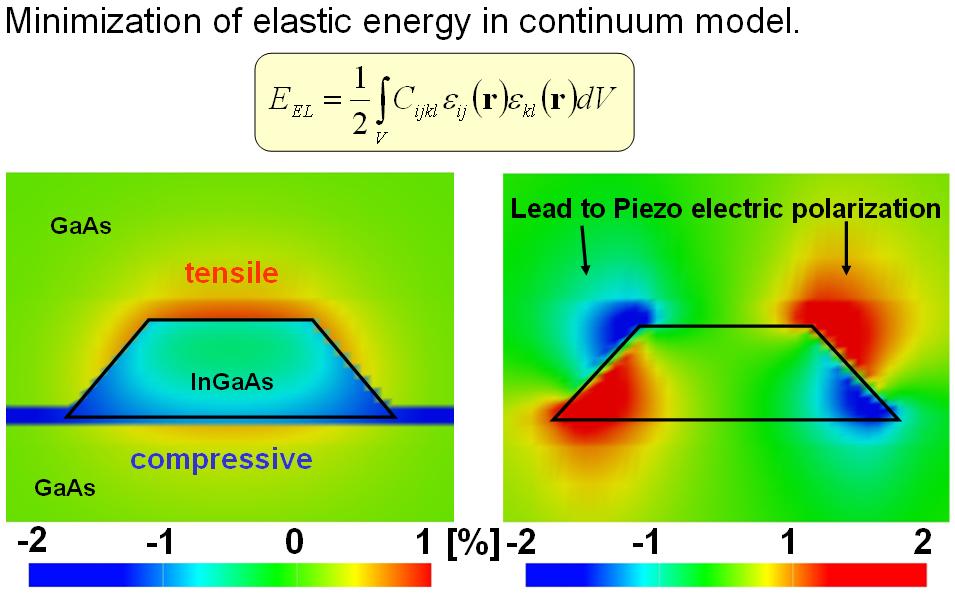
58 Electronic Structure Calculate Strain

59 Electronic Structure Calculate the Quantum States
60 Self Assembling QDs Conclusions Nanoscale islands form during strain driven self-assembly Formation is driven by thermodynamic forces Size of islands is self-limiting nm range Realised in many materials systems (e.g. InAs on (Al)GaAs, Ge on Si, InAs on InP ) Already incorporated into many optoelectronic devices Lasers, LEDs, Detectors, Non-Classical Light emitters, Hardware for quantum computation
61 Self Assembling QDs Conclusions Advantages Large confinement energies (>60meV) High crystal (optical) quality High areal density ( cm -2 ) Weak coupling to their environment Multiple layers of dots can be readily fabricated Disadvantages Homogeneity - size, shape and morphology fluctuations
62 Acknowledgement Jon Finley Dimitri Kovalev Martin Stutzmann Andreas Kress, Felix Hofbauer, Michael Kaniber WSI (E24) References: Please ask for special topics.
Self-Assembled InAs Quantum Dots
 Self-Assembled InAs Quantum Dots Steve Lyon Department of Electrical Engineering What are semiconductors What are semiconductor quantum dots How do we make (grow) InAs dots What are some of the properties
Part I. Nanostructure design and structural properties of epitaxially grown quantum dots and nanowires
 Part I Nanostructure design and structural properties of epitaxially grown quantum dots and nanowires 1 Growth of III V semiconductor quantum dots C. Schneider, S. Höfling and A. Forchel 1.1 Introduction
interband transitions in semiconductors M. Fox, Optical Properties of Solids, Oxford Master Series in Condensed Matter Physics
 interband transitions in semiconductors M. Fox, Optical Properties of Solids, Oxford Master Series in Condensed Matter Physics interband transitions in quantum wells Atomic wavefunction of carriers in
solidi current topics in solid state physics InAs quantum dots grown by molecular beam epitaxy on GaAs (211)B polar substrates
B polar substrates") solidi status physica pss c current topics in solid state physics InAs quantum dots grown by molecular beam epitaxy on GaAs (211)B polar substrates M. Zervos1, C. Xenogianni1,2, G. Deligeorgis1, M. Androulidaki1,
solidi status physica pss c current topics in solid state physics InAs quantum dots grown by molecular beam epitaxy on GaAs (211)B polar substrates M. Zervos1, C. Xenogianni1,2, G. Deligeorgis1, M. Androulidaki1,
Introduction to semiconductor nanostructures. Peter Kratzer Modern Concepts in Theoretical Physics: Part II Lecture Notes
 Introduction to semiconductor nanostructures Peter Kratzer Modern Concepts in Theoretical Physics: Part II Lecture Notes What is a semiconductor? The Fermi level (chemical potential of the electrons) falls
GeSi Quantum Dot Superlattices
 GeSi Quantum Dot Superlattices ECE440 Nanoelectronics Zheng Yang Department of Electrical & Computer Engineering University of Illinois at Chicago Nanostructures & Dimensionality Bulk Quantum Walls Quantum
Semiconductor Nanostructures. Gerhard Abstreiter
 Semiconductor Nanostructures Fabrication and Properties of Self-Assembled Quantum Dots Gerhard Abstreiter Walter Schottky Institute, TUM, Garching Gerhard Abstreiter, ICPS-27, July 25, 2004, Flagstaff
Seminars in Nanosystems - I
 Seminars in Nanosystems - I Winter Semester 2011/2012 Dr. Emanuela Margapoti Emanuela.Margapoti@wsi.tum.de Dr. Gregor Koblmüller Gregor.Koblmueller@wsi.tum.de Seminar Room at ZNN 1 floor Topics of the
III-V nanostructured materials synthesized by MBE droplet epitaxy
 III-V nanostructured materials synthesized by MBE droplet epitaxy E.A. Anyebe 1, C. C. Yu 1, Q. Zhuang 1,*, B. Robinson 1, O Kolosov 1, V. Fal ko 1, R. Young 1, M Hayne 1, A. Sanchez 2, D. Hynes 2, and
Fabrication / Synthesis Techniques
 Quantum Dots Physical properties Fabrication / Synthesis Techniques Applications Handbook of Nanoscience, Engineering, and Technology Ch.13.3 L. Kouwenhoven and C. Marcus, Physics World, June 1998, p.35
Quantum Dot Lasers. Jose Mayen ECE 355
 Quantum Dot Lasers Jose Mayen ECE 355 Overview of Presentation Quantum Dots Operation Principles Fabrication of Q-dot lasers Advantages over other lasers Characteristics of Q-dot laser Types of Q-dot lasers
Photonic devices for quantum information processing:
 Outline Photonic devices for quantum information processing: coupling to dots, structure design and fabrication Optoelectronics Group, Cavendish Lab Outline Vuckovic s group Noda s group Outline Outline
Three-Dimensional Silicon-Germanium Nanostructures for Light Emitters and On-Chip Optical. Interconnects
 Three-Dimensional Silicon-Germanium Nanostructures for Light Emitters and On-Chip Optical eptember 2011 Interconnects Leonid Tsybeskov Department of Electrical and Computer Engineering New Jersey Institute
Single Photon Generation & Application
 Single Photon Generation & Application Photon Pair Generation: Parametric down conversion is a non-linear process, where a wave impinging on a nonlinear crystal creates two new light beams obeying energy
Using Light to Prepare and Probe an Electron Spin in a Quantum Dot
 A.S. Bracker, D. Gammon, E.A. Stinaff, M.E. Ware, J.G. Tischler, D. Park, A. Shabaev, and A.L. Efros Using Light to Prepare and Probe an Electron Spin in a Quantum Dot A.S. Bracker, D. Gammon, E.A. Stinaff,
Nanoscience galore: hybrid and nanoscale photonics
 Nanoscience galore: hybrid and nanoscale photonics Pavlos Lagoudakis SOLAB, 11 June 2013 Hybrid nanophotonics Nanostructures: light harvesting and light emitting devices 2 Hybrid nanophotonics Nanostructures:
Electron Energy, E E = 0. Free electron. 3s Band 2p Band Overlapping energy bands. 3p 3s 2p 2s. 2s Band. Electrons. 1s ATOM SOLID.
 Electron Energy, E Free electron Vacuum level 3p 3s 2p 2s 2s Band 3s Band 2p Band Overlapping energy bands Electrons E = 0 1s ATOM 1s SOLID In a metal the various energy bands overlap to give a single
Quantum Dot Lasers. Andrea Fiore. Ecole Polytechnique Fédérale de Lausanne
 Quantum Dot Lasers Ecole Polytechnique Fédérale de Lausanne Outline: Quantum-confined active regions Self-assembled quantum dots Laser applications Electronic states in semiconductors Schrödinger eq.:
Novel materials and nanostructures for advanced optoelectronics
 Novel materials and nanostructures for advanced optoelectronics Q. Zhuang, P. Carrington, M. Hayne, A Krier Physics Department, Lancaster University, UK u Brief introduction to Outline Lancaster University
Quantum Dots for Advanced Research and Devices
 Quantum Dots for Advanced Research and Devices spectral region from 450 to 630 nm Zero-D Perovskite Emit light at 520 nm ABOUT QUANTUM SOLUTIONS QUANTUM SOLUTIONS company is an expert in the synthesis
Influence of hyperfine interaction on optical orientation in self-assembled InAs/GaAs quantum dots
 Influence of hyperfine interaction on optical orientation in self-assembled InAs/GaAs quantum dots O. Krebs, B. Eble (PhD), S. Laurent (PhD), K. Kowalik (PhD) A. Kudelski, A. Lemaître, and P. Voisin Laboratoire
Optical Characterization of Self-Assembled Si/SiGe Nano-Structures
 Optical Characterization of Self-Assembled Si/SiGe Nano-Structures T. Fromherz, W. Mac, G. Bauer Institut für Festkörper- u. Halbleiterphysik, Johannes Kepler Universität Linz, Altenbergerstraße 69, A-
Luminescence Process
 Luminescence Process The absorption and the emission are related to each other and they are described by two terms which are complex conjugate of each other in the interaction Hamiltonian (H er ). In an
Photonic Crystal Nanocavities for Efficient Light Confinement and Emission
 Journal of the Korean Physical Society, Vol. 42, No., February 2003, pp. 768 773 Photonic Crystal Nanocavities for Efficient Light Confinement and Emission Axel Scherer, T. Yoshie, M. Lončar, J. Vučković
Lecture 3: Heterostructures, Quasielectric Fields, and Quantum Structures
 Lecture 3: Heterostructures, Quasielectric Fields, and Quantum Structures MSE 6001, Semiconductor Materials Lectures Fall 2006 3 Semiconductor Heterostructures A semiconductor crystal made out of more
Semiconductor Quantum Dot Nanostructures and their Roles in the Future of Photonics
 550 Brazilian Journal of Physics, vol. 34, no. 2B, June, 2004 Semiconductor Quantum Dot Nanostructures and their Roles in the Future of Photonics S. Fafard, K. Hinzer, and C. N. Allen Institute for Microstructural
Investigation of the formation of InAs QD's in a AlGaAs matrix
 10th Int. Symp. "Nanostructures: Physics and Technology" St Petersburg, Russia, June 17-21, 2002 2002 IOFFE Institute NT.16p Investigation of the formation of InAs QD's in a AlGaAs matrix D. S. Sizov,
Emission Spectra of the typical DH laser
 Emission Spectra of the typical DH laser Emission spectra of a perfect laser above the threshold, the laser may approach near-perfect monochromatic emission with a spectra width in the order of 1 to 10
1 Semiconductor Quantum Dots for Ultrafast Optoelectronics
 j1 1 Semiconductor Quantum Dots for Ultrafast Optoelectronics 1.1 The Role of Dimensionality in Semiconductor Materials The history of semiconductor lasers has been punctuated by dramatic revolutions.
Semiconductor quantum dots
 Semiconductor quantum dots Quantum dots are spherical nanocrystals of semiconducting materials constituted from a few hundreds to a few thousands atoms, characterized by the quantum confinement of the
Optical Investigation of the Localization Effect in the Quantum Well Structures
 Department of Physics Shahrood University of Technology Optical Investigation of the Localization Effect in the Quantum Well Structures Hamid Haratizadeh hamid.haratizadeh@gmail.com IPM, SCHOOL OF PHYSICS,
Chapter 3 Properties of Nanostructures
 Chapter 3 Properties of Nanostructures In Chapter 2, the reduction of the extent of a solid in one or more dimensions was shown to lead to a dramatic alteration of the overall behavior of the solids. Generally,
Laser Basics. What happens when light (or photon) interact with a matter? Assume photon energy is compatible with energy transition levels.
 interact with a matter? Assume photon energy is compatible with energy transition levels.") What happens when light (or photon) interact with a matter? Assume photon energy is compatible with energy transition levels. Electron energy levels in an hydrogen atom n=5 n=4 - + n=3 n=2 13.6 = [ev]
What happens when light (or photon) interact with a matter? Assume photon energy is compatible with energy transition levels. Electron energy levels in an hydrogen atom n=5 n=4 - + n=3 n=2 13.6 = [ev]
Nanostrutture a confinamento quantistico elettronico: i quantum dot
 Nanostrutture a confinamento quantistico elettronico: i quantum dot Massimo De Vittorio National Nanotechnology Laboratories of CNR-INFM ISUFI - Università del Salento massimo.devittorio@unile.it Outline
Light Interaction with Small Structures
 Light Interaction with Small Structures Molecules Light scattering due to harmonically driven dipole oscillator Nanoparticles Insulators Rayleigh Scattering (blue sky) Semiconductors...Resonance absorption
Widely Tunable and Intense Mid-Infrared PL Emission from Epitaxial Pb(Sr)Te Quantum Dots in a CdTe Matrix
Te Quantum Dots in a CdTe Matrix") Widely Tunable and Intense Mid-Infrared PL Emission from Epitaxial Pb(Sr)Te Quantum Dots in a Matrix S. Kriechbaumer 1, T. Schwarzl 1, H. Groiss 1, W. Heiss 1, F. Schäffler 1,T. Wojtowicz 2, K. Koike 3,
Widely Tunable and Intense Mid-Infrared PL Emission from Epitaxial Pb(Sr)Te Quantum Dots in a Matrix S. Kriechbaumer 1, T. Schwarzl 1, H. Groiss 1, W. Heiss 1, F. Schäffler 1,T. Wojtowicz 2, K. Koike 3,
what happens if we make materials smaller?
 what happens if we make materials smaller? IAP VI/10 ummer chool 2007 Couvin Prof. ns outline Introduction making materials smaller? ynthesis how do you make nanomaterials? Properties why would you make
Metal Vapour Lasers Use vapoured metal as a gain medium Developed by W. Silfvast (1966) Two types: Ionized Metal vapour (He-Cd) Neutral Metal vapour
 Two types: Ionized Metal vapour (He-Cd) Neutral Metal vapour") Metal Vapour Lasers Use vapoured metal as a gain medium Developed by W. Silfvast (1966) Two types: Ionized Metal vapour (He-Cd) Neutral Metal vapour (Cu) All operate by vaporizing metal in container Helium
Metal Vapour Lasers Use vapoured metal as a gain medium Developed by W. Silfvast (1966) Two types: Ionized Metal vapour (He-Cd) Neutral Metal vapour (Cu) All operate by vaporizing metal in container Helium
Physics and Material Science of Semiconductor Nanostructures
 Physics and Material Science of Semiconductor Nanostructures PHYS 570P Prof. Oana Malis Email: omalis@purdue.edu Course website: http://www.physics.purdue.edu/academic_programs/courses/phys570p/ 1 Introduction
Raman spectroscopy of self-assembled InAs quantum dots in wide-bandgap matrices of AlAs and aluminium oxide
 Mat. Res. Soc. Symp. Proc. Vol. 737 2003 Materials Research Society E13.8.1 Raman spectroscopy of self-assembled InAs quantum dots in wide-bandgap matrices of AlAs and aluminium oxide D. A. Tenne, A. G.
Physics and Material Science of Semiconductor Nanostructures
 Physics and Material Science of Semiconductor Nanostructures PHYS 570P Prof. Oana Malis Email: omalis@purdue.edu Course website: http://www.physics.purdue.edu/academic_programs/courses/phys570p/ 1 Course
Solar Cell Materials and Device Characterization
 Solar Cell Materials and Device Characterization April 3, 2012 The University of Toledo, Department of Physics and Astronomy SSARE, PVIC Principles and Varieties of Solar Energy (PHYS 4400) and Fundamentals
Time resolved optical spectroscopy methods for organic photovoltaics. Enrico Da Como. Department of Physics, University of Bath
 Time resolved optical spectroscopy methods for organic photovoltaics Enrico Da Como Department of Physics, University of Bath Outline Introduction Why do we need time resolved spectroscopy in OPV? Short
Optical Spectroscopies of Thin Films and Interfaces. Dietrich R. T. Zahn Institut für Physik, Technische Universität Chemnitz, Germany
 Optical Spectroscopies of Thin Films and Interfaces Dietrich R. T. Zahn Institut für Physik, Technische Universität Chemnitz, Germany 1. Introduction 2. Vibrational Spectroscopies (Raman and Infrared)
In a metal, how does the probability distribution of an electron look like at absolute zero?
 1 Lecture 6 Laser 2 In a metal, how does the probability distribution of an electron look like at absolute zero? 3 (Atom) Energy Levels For atoms, I draw a lower horizontal to indicate its lowest energy
OPTICAL PROPERTIES AND SPECTROSCOPY OF NANOAAATERIALS. Jin Zhong Zhang. World Scientific TECHNISCHE INFORMATIONSBIBLIOTHEK
 OPTICAL PROPERTIES AND SPECTROSCOPY OF NANOAAATERIALS Jin Zhong Zhang University of California, Santa Cruz, USA TECHNISCHE INFORMATIONSBIBLIOTHEK Y World Scientific NEW JERSEY. t'on.don SINGAPORE «'BEIJING
Electronic and Optoelectronic Properties of Semiconductor Structures
 Electronic and Optoelectronic Properties of Semiconductor Structures Jasprit Singh University of Michigan, Ann Arbor CAMBRIDGE UNIVERSITY PRESS CONTENTS PREFACE INTRODUCTION xiii xiv 1.1 SURVEY OF ADVANCES
Review of Optical Properties of Materials
 Review of Optical Properties of Materials Review of optics Absorption in semiconductors: qualitative discussion Derivation of Optical Absorption Coefficient in Direct Semiconductors Photons When dealing
Femtosecond nonlinear coherence spectroscopy of carrier dynamics in porous silicon
 JOURNAL OF APPLIED PHYSICS 98, 083508 2005 Femtosecond nonlinear coherence spectroscopy of carrier dynamics in porous silicon Lap Van Dao a and Peter Hannaford Centre for Atom Optics and Ultrafast Spectroscopy,
EECS143 Microfabrication Technology
 EECS143 Microfabrication Technology Professor Ali Javey Introduction to Materials Lecture 1 Evolution of Devices Yesterday s Transistor (1947) Today s Transistor (2006) Why Semiconductors? Conductors e.g
Heterostructures and sub-bands
 Heterostructures and sub-bands (Read Datta 6.1, 6.2; Davies 4.1-4.5) Quantum Wells In a quantum well, electrons are confined in one of three dimensions to exist within a region of length L z. If the barriers
Chapter 6 Photoluminescence Spectroscopy
 Chapter 6 Photoluminescence Spectroscopy Course Code: SSCP 4473 Course Name: Spectroscopy & Materials Analysis Sib Krishna Ghoshal (PhD) Advanced Optical Materials Research Group Physics Department, Faculty
Electroluminescence from Silicon and Germanium Nanostructures
 Electroluminescence from silicon Silicon Getnet M. and Ghoshal S.K 35 ORIGINAL ARTICLE Electroluminescence from Silicon and Germanium Nanostructures Getnet Melese* and Ghoshal S. K.** Abstract Silicon
Luminescence basics. Slide # 1
 Luminescence basics Types of luminescence Cathodoluminescence: Luminescence due to recombination of EHPs created by energetic electrons. Example: CL mapping system Photoluminescence: Luminescence due to
QUANTUM NANOSTRUCTURES
 QUANTUM NANOSTRUCTURES by Droplet Epitaxy Somsak Panyakeow Semiconductor Device Research Laboratory (SDRL), CoE Nanotechnology Center of Thailand, Department of Electrical Engineering, Faculty of Engineering,
Intraband emission of GaN quantum dots at λ =1.5 μm via resonant Raman scattering
 Intraband emission of GaN quantum dots at λ =1.5 μm via resonant Raman scattering L. Nevou, F. H. Julien, M. Tchernycheva, J. Mangeney Institut d Electronique Fondamentale, UMR CNRS 8622, University Paris-Sud
Quantum Dots The Pennsylvania State University Quantum Dots 1
 Quantum Dots www.nano4me.org 2018 The Pennsylvania State University Quantum Dots 1 Outline Introduction Quantum Confinement QD Synthesis Colloidal Methods Epitaxial Growth Applications Biological Light
Crystal Properties. MS415 Lec. 2. High performance, high current. ZnO. GaN
 Crystal Properties Crystal Lattices: Periodic arrangement of atoms Repeated unit cells (solid-state) Stuffing atoms into unit cells Determine mechanical & electrical properties High performance, high current
Quantum Condensed Matter Physics Lecture 12
 Quantum Condensed Matter Physics Lecture 12 David Ritchie QCMP Lent/Easter 2016 http://www.sp.phy.cam.ac.uk/drp2/home 12.1 QCMP Course Contents 1. Classical models for electrons in solids 2. Sommerfeld
(002)(110) (004)(220) (222) (112) (211) (202) (200) * * 2θ (degree)
(110) (004)(220) (222) (112) (211) (202) (200) * * 2θ (degree)") Supplementary Figures. (002)(110) Tetragonal I4/mcm Intensity (a.u) (004)(220) 10 (112) (211) (202) 20 Supplementary Figure 1. X-ray diffraction (XRD) pattern of the sample. The XRD characterization indicates
Supplementary Figures. (002)(110) Tetragonal I4/mcm Intensity (a.u) (004)(220) 10 (112) (211) (202) 20 Supplementary Figure 1. X-ray diffraction (XRD) pattern of the sample. The XRD characterization indicates
Conductivity and Semi-Conductors
 Conductivity and Semi-Conductors J = current density = I/A E = Electric field intensity = V/l where l is the distance between two points Metals: Semiconductors: Many Polymers and Glasses 1 Electrical Conduction
Nano-optics. Topics: How do we image things on the nanoscale? How do we use nanofabrication for new optical devices? COSMOS 2006 Lecture 1
 Nano-optics Topics: How do we image things on the nanoscale? How do we use nanofabrication for new optical devices? Wave Optics 1. Electromagnetic wave x Ex λ Direction of Propagation y z z plane wave
Stimulated Emission Devices: LASERS
 Stimulated Emission Devices: LASERS 1. Stimulated Emission and Photon Amplification E 2 E 2 E 2 hυ hυ hυ In hυ Out hυ E 1 E 1 E 1 (a) Absorption (b) Spontaneous emission (c) Stimulated emission The Principle
Supplementary Materials
 Supplementary Materials Sample characterization The presence of Si-QDs is established by Transmission Electron Microscopy (TEM), by which the average QD diameter of d QD 2.2 ± 0.5 nm has been determined
Fabrication at the nanoscale for nanophotonics
 Fabrication at the nanoscale for nanophotonics Ilya Sychugov, KTH Materials Physics, Kista silicon nanocrystal by electron beam induced deposition lithography Outline of basic nanofabrication methods Devices
SELF-ASSEMBLED QUANTUM DOTS FOR OPTOELECTRONIC DEVICES: PROGRESS AND CHALLENGES
 SELF-ASSEMBLED QUANTUM DOTS FOR OPTOELECTRONIC DEVICES: PROGRESS AND CHALLENGES M.Henini School of Physics and Astronomy, University of Nottingham, Nottingham NG7 2RD, U.K. Tel/Fax: +44 115 9515195/9515180
Scienza e Tecnologia dei Materiali Ceramici. Modulo 2: Materiali Nanostrutturati
 Università degli Studi di Trieste Dipartimento di Ingegneria e Architettura A.A. 2016-2017 Scienza e Tecnologia dei Materiali Ceramici Modulo 2: Materiali Nanostrutturati - Lezione 5 - Vanni Lughi vlughi@units.it
The Electromagnetic Properties of Materials
 The Electromagnetic Properties of Materials Electrical conduction Metals Semiconductors Insulators (dielectrics) Superconductors Magnetic materials Ferromagnetic materials Others Photonic Materials (optical)
Lecture 20: Semiconductor Structures Kittel Ch 17, p , extra material in the class notes
 Lecture 20: Semiconductor Structures Kittel Ch 17, p 494-503, 507-511 + extra material in the class notes MOS Structure Layer Structure metal Oxide insulator Semiconductor Semiconductor Large-gap Semiconductor
Fluorescence Spectroscopy
 Fluorescence Spectroscopy Frequency and time dependent emission Emission and Excitation fluorescence spectra Stokes Shift: influence of molecular vibrations and solvent Time resolved fluorescence measurements
Chemistry Instrumental Analysis Lecture 8. Chem 4631
 Chemistry 4631 Instrumental Analysis Lecture 8 UV to IR Components of Optical Basic components of spectroscopic instruments: stable source of radiant energy transparent container to hold sample device
Single Semiconductor Nanostructures for Quantum Photonics Applications: A solid-state cavity-qed system with semiconductor quantum dots
 The 3 rd GCOE Symposium 2/17-19, 19, 2011 Tohoku University, Sendai, Japan Single Semiconductor Nanostructures for Quantum Photonics Applications: A solid-state cavity-qed system with semiconductor quantum
Physics of Semiconductors (Problems for report)
") Physics of Semiconductors (Problems for report) Shingo Katsumoto Institute for Solid State Physics, University of Tokyo July, 0 Choose two from the following eight problems and solve them. I. Fundamentals
Physics of Semiconductors (Problems for report) Shingo Katsumoto Institute for Solid State Physics, University of Tokyo July, 0 Choose two from the following eight problems and solve them. I. Fundamentals
GISAXS, GID and X-Ray Reflectivity in Materials Science
 united nations educational, scientific and cultural organization the abdus salam international centre for theoretical physics international atomic energy agency SCHOOL ON SYNCHROTRON RADIATION AND APPLICATIONS
Broadband Quantum-Dot/Dash Lasers
 Broadband Quantum-Dot/Dash Lasers Boon S. Ooi, Electrical & Computer Eng. Lehigh University Tel: 610-758 2606, email:bsooi@lehigh.edu ACKNOWDLEDGEMENT Students and Postdoc: Hery S. Djie, Yang Wang, Clara
Contents Part I Concepts 1 The History of Heterostructure Lasers 2 Stress-Engineered Quantum Dots: Nature s Way
 Contents Part I Concepts 1 The History of Heterostructure Lasers Zhores I. Alferov... 3 1.1 Introduction... 3 1.2 The DHS Concept and Its Application for Semiconductor Lasers. 3 1.3 Quantum Dot Heterostructure
SUPPLEMENTARY INFORMATION
 doi:10.1038/nature12036 We provide in the following additional experimental data and details on our demonstration of an electrically pumped exciton-polariton laser by supplementing optical and electrical
Study on Quantum Dot Lasers and their advantages
 Study on Quantum Dot Lasers and their advantages Tae Woo Kim Electrical and Computer Engineering University of Illinois, Urbana Champaign Abstract Basic ideas for understanding a Quantum Dot Laser were
EE143 Fall 2016 Microfabrication Technologies. Evolution of Devices
 EE143 Fall 2016 Microfabrication Technologies Prof. Ming C. Wu wu@eecs.berkeley.edu 511 Sutardja Dai Hall (SDH) 1-1 Evolution of Devices Yesterday s Transistor (1947) Today s Transistor (2006) 1-2 1 Why
Spin Dynamics in Single GaAs Nanowires
 1 Dr. Max Mustermann Referat Kommunikation & Marketing Verwaltung Spin Dynamics in Single GaAs Nanowires F. Dirnberger, S. Furthmeier, M. Forsch, A. Bayer, J. Hubmann, B. Bauer, J. Zweck, E. Reiger, C.
Spectroscopy at nanometer scale
 Spectroscopy at nanometer scale 1. Physics of the spectroscopies 2. Spectroscopies for the bulk materials 3. Experimental setups for the spectroscopies 4. Physics and Chemistry of nanomaterials Various
Optical Properties of Solid from DFT
 Optical Properties of Solid from DFT 1 Prof.P. Ravindran, Department of Physics, Central University of Tamil Nadu, India & Center for Materials Science and Nanotechnology, University of Oslo, Norway http://folk.uio.no/ravi/cmt15
LEC E T C U T R U E R E 17 -Photodetectors
 LECTURE 17 -Photodetectors Topics to be covered Photodetectors PIN photodiode Avalanche Photodiode Photodetectors Principle of the p-n junction Photodiode A generic photodiode. Photodetectors Principle
Graphene and Carbon Nanotubes
 Graphene and Carbon Nanotubes 1 atom thick films of graphite atomic chicken wire Novoselov et al - Science 306, 666 (004) 100μm Geim s group at Manchester Novoselov et al - Nature 438, 197 (005) Kim-Stormer
Semiconductor Fundamentals. Professor Chee Hing Tan
 Semiconductor Fundamentals Professor Chee Hing Tan c.h.tan@sheffield.ac.uk Why use semiconductor? Microprocessor Transistors are used in logic circuits that are compact, low power consumption and affordable.
1. Nanotechnology & nanomaterials -- Functional nanomaterials enabled by nanotechnologies.
 Novel Nano-Engineered Semiconductors for Possible Photon Sources and Detectors NAI-CHANG YEH Department of Physics, California Institute of Technology 1. Nanotechnology & nanomaterials -- Functional nanomaterials
Physics and Material Science of Semiconductor Nanostructures
 Physics and Material Science of Semiconductor Nanostructures PHYS 570P Prof. Oana Malis Email: omalis@purdue.edu Course website: http://www.physics.purdue.edu/academic_programs/courses/phys570p/ Lecture
TECHNICAL INFORMATION. Quantum Dot
 Quantum Dot Quantum Dot is the nano meter sized semiconductor crystal with specific optical properties originates from the phenomenon which can be explained by the quantum chemistry and quantum mechanics.
OPTI510R: Photonics. Khanh Kieu College of Optical Sciences, University of Arizona Meinel building R.626
 OPTI510R: Photonics Khanh Kieu College of Optical Sciences, University of Arizona kkieu@optics.arizona.edu Meinel building R.626 Announcements HW#3 is assigned due Feb. 20 st Mid-term exam Feb 27, 2PM
Optical Properties of Semiconductors. Prof.P. Ravindran, Department of Physics, Central University of Tamil Nadu, India
 Optical Properties of Semiconductors 1 Prof.P. Ravindran, Department of Physics, Central University of Tamil Nadu, India http://folk.uio.no/ravi/semi2013 Light Matter Interaction Response to external electric
PHOTOLUMINESCENCE STUDY OF INGAAS/GAAS QUANTUM DOTS
 PHOTOLUMINESCENCE STUDY OF INGAAS/GAAS QUANTUM DOTS A. Majid a,b, Samir Alzobaidi a and Thamer Alharbi a a Department of Physics, College of Science, Almajmaah University, P. O. Box no.1712, Al-Zulfi 11932,
Single Photon detectors
 Single Photon detectors Outline Motivation for single photon detection Semiconductor; general knowledge and important background Photon detectors: internal and external photoeffect Properties of semiconductor
Teaching Nanomagnets New Tricks
 Teaching Nanomagnets New Tricks v / Igor Zutic R. Oszwaldowski, J. Pientka, J. Han, University at Buffalo, State University at New York A. Petukhov, South Dakota School Mines & Technology P. Stano, RIKEN
Temperature Dependent Optical Band Gap Measurements of III-V films by Low Temperature Photoluminescence Spectroscopy
 Temperature Dependent Optical Band Gap Measurements of III-V films by Low Temperature Photoluminescence Spectroscopy Linda M. Casson, Francis Ndi and Eric Teboul HORIBA Scientific, 3880 Park Avenue, Edison,
White light from solid state sources. Stephen Mullens
 White light from solid state sources Stephen Mullens Abstract The human perception of colour is paramount to the production of white light sources. Historical lighting technologies such as incandescence
Lecture 6: Individual nanoparticles, nanocrystals and quantum dots
 Lecture 6: Individual nanoparticles, nanocrystals and quantum dots Definition of nanoparticle: Size definition arbitrary More interesting: definition based on change in physical properties. Size smaller
EECS130 Integrated Circuit Devices
 EECS130 Integrated Circuit Devices Professor Ali Javey 8/30/2007 Semiconductor Fundamentals Lecture 2 Read: Chapters 1 and 2 Last Lecture: Energy Band Diagram Conduction band E c E g Band gap E v Valence
(b) Spontaneous emission. Absorption, spontaneous (random photon) emission and stimulated emission.
 Spontaneous emission. Absorption, spontaneous (random photon) emission and stimulated emission.") Lecture 10 Stimulated Emission Devices Lasers Stimulated emission and light amplification Einstein coefficients Optical fiber amplifiers Gas laser and He-Ne Laser The output spectrum of a gas laser Laser
Lecture 10 Stimulated Emission Devices Lasers Stimulated emission and light amplification Einstein coefficients Optical fiber amplifiers Gas laser and He-Ne Laser The output spectrum of a gas laser Laser
Developing Quantum Logic Gates: Spin-Resonance-Transistors
 Developing Quantum Logic Gates: Spin-Resonance-Transistors H. W. Jiang (UCLA) SRT: a Field Effect Transistor in which the channel resistance monitors electron spin resonance, and the resonance frequency
The Use of Synchrotron Radiation in Modern Research
 The Use of Synchrotron Radiation in Modern Research Physics Chemistry Structural Biology Materials Science Geochemical and Environmental Science Atoms, molecules, liquids, solids. Electronic and geometric