Nanostrutture a confinamento quantistico elettronico: i quantum dot
|
|
|
- Baldwin West
- 6 years ago
- Views:
Transcription


1 Nanostrutture a confinamento quantistico elettronico: i quantum dot Massimo De Vittorio National Nanotechnology Laboratories of CNR-INFM ISUFI - Università del Salento massimo.devittorio@unile.it
2 Outline Properties of quantum dots (QDs) Synthesis of quantum dots Self organized epitaxial quantum dots Colloidal quantum dots Device and applications of different types of quantum dots Conclusions
 Discrete states (Artificial atoms) Quasi zero-dimensional systems")
3 What is a quantum dot A confining potential in three dimensions whose size has no sharp definitions Wave nature of carriers is important (of the order De Broglie wavelength 10 nm in InAs) Discrete states (Artificial atoms) Quasi zero-dimensional systems
 with uniform composition")

4 The ideal QDs Precise size and shape (box or sphere) with uniform composition Infinite quantum confinement Array of identical quantum dot For a cubic dot (size L):
5
6 Applications of epitaxial QDs Improve existing devices: Lasers and MCLEDs Optical amplifiers Long Wavelength detectors Novel devices and applications Spintronics Quantum computing Quantum cryptography (single photon emitters) Optical memories Unique physics compared to bulk semiconductors materials


7 SEMICONDUCTOR QUANTUM DOTS BASED PHOTONIC DEVICES Telecommunications and information technology demand fast and reliable data exchange on wide-world area networks Display and Lightning technology looking for bright, high-resolution, multi-color or white emitting light sources Pioneering studies on quantum cryptography and non-classical photon sources Development of optical data transmission systems requiring: - low-cost μm emitting - spectrally pure - low-power operating - temperature insensitive - fast modulating Development of: - cheap - spectrally tunable - long-lasting - bright - controlled at micron-scale Development of: - reliable - spectrally ultra-pure - long-lasting - room-temperature working
8 Synthesis of QDs Top-down approach Self-organization: Stranski Krastanov epitaxial growth Colloidal quantum dots
")

9 Top-down approach for QDs slow process, difficult to have large amount of QDs Uniform QDs (limit by litography) Defect states at interfaces due to etching Bottom-up synthesis of QDs Colloidal quantum dots Stranski Krastanov epitaxial growth
 pyramidal-shaped or lens-shaped islands; lateral size ~ 10 40 nm and heights ~5 8 nm room-temperature emission")


10 Bottom-up synthesis of QDs Stranski-Krastanow growth Wet-chemical synthesis Growth facilities: Metal-Organic Chemical Vapor Deposition (MOCVD) /Molecular Beam Epitaxy (MBE) pyramidal-shaped or lens-shaped islands; lateral size ~ nm and heights ~5 8 nm room-temperature emission from single QD difficult to be achieved due to phonons energy comparable with allowed energy levels distance complete burying of QDs into solid crystalline matrix: low surface defects, high photostability, high radiative recombination rates efficient electrical injection by p-n doping of the surrounding heterostructure size fluctuation in QD layers: inhomogeneous broadening Growth facilities: Schlenk line, liquid solution / Low-cost and high throughput fabrication method spherical shape with diameter ~ 2-6 nm higher distance among allowed energy states in conduction and valence bands: intense emission also at room temperature lack of a solid matrix: spectral shifting and blinking of the single emitter / Need to insert QDs from liquid solution to solid matrices easy optical pumping / not straightforward electrical pumping inhomogeneous broadening


11 Epitaxial growth techniques: MOCVD e MBE Differences: Growth rate UHV and situ monitoring safety and materials

 2D epitaxial growth:")

12 Self assembled QDs Epitaxial growth: Interplay of surface energy and strain "Standard" (Frank-van der Merve) 2D epitaxial growth: GaAs Substrate AlAs Stranski-Krastanov 3D growth mode (strain-driven): InAs Substrate
13 MOCVD QDs

14 EFFECT OF THE GROWTH RATE

15 Effect of the Growth Temperature
16 Synthesis of Colloidal Quantum dots


17 Synthesis of colloidal nanocrystals Ar Ar thermocouple Heating mantle Mixture of surfactants Inject organometalli c precursors high T, C 350 set 348 cur temperature controller Highly crystalline Narrow size distribution


18 Size dependent photoluminescence absorption / emission of CdSe nanocrystals relative narrow emission (30-35 nm fwhm) no red-tail wavelength [nm] all colors can be excited with one single wavelength


19 Nanocrystal size control: Colloidal nanocrystals of different materials ZnSe PbSe CdSe nanocrystals Fe 2 O 3 CoPt 3
20 Epitaxial quantum dot devices for telecom applications


21 Single-mode QD lasers internal losses of 4.8 cm-1 internal quantum efficiency of 23% The saturation modal gain of the ground state results to be 36.3 cm -1 6 cm -1 per QD layer Device cross-section acquired by SEM
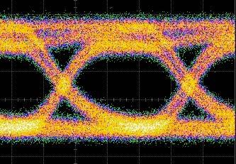
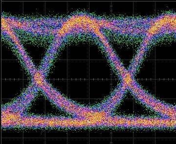
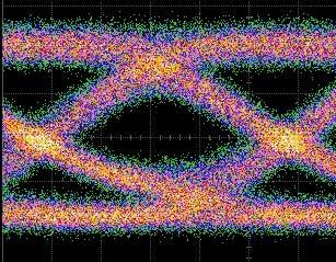
22 High modulation frequency eye patterns 15 C 85 C 15 C 50 C
23 Emitted photons Single photons from single QDs time QD Quantum cryptography: Alice Bob Single- source Eve

24 The image cannot be displayed. Your computer may not have enough memory to open the image, or the image may have been corrupted. Restart your computer, and then open the file again. If the red x still appears, you may have to delete the image and then insert it again. Single QD devices Shadow-mask LED: diffusion suppressed (<100 nm) in QDs due to carrier confinement 300 nm current aperture oxid. edge oxid. edge Down to 100 nm current apertures with simple optical lithography Can tailor both current and optical confinement Bandgap engineering to reduce current spreading Fiore et al., Appl. Phys. Lett. 2002
25 Colloidal NCs devices and applications


26 Solar Cells h+ e- I T O Al Molecular Recognition Fundamental studies Nanocrystals Light Emitting Diodes Mg/Ag PPV ITO Single-Electron Transistors Biological Labels Catalysts Sensors

27 Hybrid nanocomposites: magnetic and fluorescent properties combined into one single nano-object A. Quarta, R. Di Corato, L. Manna andt. Pellegrino, Fluorescent magnetic hybrid nanostructures: preparation, properties and applications in biology, IEEE Transaction in Nanobiotechnology, in press

28 NCs dispersed in resist (ER) matrix + CdSe/ZnS nanocrystals Gain material deposited by means of low-cost techniques poly(methylmethacrylate) SU-8(epoxy resist) Sensitive to electron beam or UV radiation Highly versatile active material for optical devices - Decoupled synthesis of NCs from preparation of matrix - Complete tunability of optical properties from UV to IR range - Full control on the device geometry/selective localization of emitters with nanometer scale resolution


29 Building blocks for photonic devices Distributed Feedback structures Waveguides Nanocavities Distributed Bragg reflectors


30 Building blocks for photonic devices PMMA/NCs Waveguides SU-8/NCs L.Pang et al., Photosensitive quantum dot composites and their applications in optical structures, J. Vac. Sci. Technol. B 23, p (2005)
 Thermoplastic behavior of PMMA")

31 Colloidal QDs: vertical microcavity by hot embossing Unconventional use of hot embossing techniques Colloidal CdSe/ZnS nanocrystals dispersed in a polymeric matrix (PMMA) Thermoplastic behavior of PMMA exploited in order to define the device geometry High-temperature exposure: 10 to 180 C No damage of the optical properties of QDs Insertion of SU-8 spacers between the mirrors Good control of the cavity length L c

32 Colloidal QDs: hybrid vertical microcavity by hot embossing Light output 40 nm 4.15 nm PMMA+NCs


33 Localization of NCs by EBL processes Blend deposition EBL exposure Blend Blend development - - Polymer/NCs blend still behaves as a resist Emission properties of NCs must not be affected by electron beam exposures RAITH 150 L. Martiradonna et al., Microelectron. Eng., 83, , 2006.


34 SEM and AFM images of patterned blend Stripes: width=2μm period=4μm Pillars: diameter=0.6μm Period=2μm The positive resist behaviour of PMMA is not perturbed by the presence of NCs


35 Photoluminescence maps by confocal microscope The PL emission signal is detected spectrum only of NCs in the is not unexposed affected regions by EBL L. Martiradonna et al., Physica Status Solidi B
36 NCs localization by lithographic techniques Several advantages: - any kind of substrate without recurring to chemical or physical treatment of the surfaces; - not only rigid substrates but also flexible devices; - the typical resolution is defined by the lithographic process; - the density of emitters can be easily tuned by varying the relative molar concentration of the two components (NCs resist); - processing by standard photolithographic techniques; - refractive index of the blend tunable with the NCs concentration.


37 Colloidal QDs: Patterning of colloidal QDs by lithographic techniques Building blocks for photonic devices DFB L BRAGG = 245 nm thk = 40 nm DBR 3 /4 stripes thk = 400nm


38 Easy implementation of multi-wavelength devices lithographic process on 1 st NCs ensemble aligned lithographic process on 2 nd NCs ensemble Re-aligned lithography Localization of NCs emitting at different wavelengths on near or superimposed regions
 - 2 nd lithography: SU-8/green NCs ( peak =550 nm, M NCs =7.")
39 Easy implementation of multi-wavelength devices 600 μm - 1 st lithography: SU-8/red NCs ( peak =640 nm, M NCs = mol/l) - 2 nd lithography: SU-8/green NCs ( peak =550 nm, M NCs = mol/l)
 - 2 nd photolithography: SU-8/green NCs ( peak =550 nm, M NCs =7.")
40 Easy implementation of multi-wavelength devices 600 μm - 1 st e-beam lithography: PMMA/red NCs ( peak =640 nm, M NCs = mol/l) - 2 nd photolithography: SU-8/green NCs ( peak =550 nm, M NCs = mol/l)


41 Easy implementation of multi-wavelength devices Single colour nanopixels Multicoloured nanopixels White emitting nanopixels Relative intensities of R, G and B tunable with NCs concentration and pattern dimensions
Fabrication / Synthesis Techniques
 Quantum Dots Physical properties Fabrication / Synthesis Techniques Applications Handbook of Nanoscience, Engineering, and Technology Ch.13.3 L. Kouwenhoven and C. Marcus, Physics World, June 1998, p.35
Self-Assembled InAs Quantum Dots
 Self-Assembled InAs Quantum Dots Steve Lyon Department of Electrical Engineering What are semiconductors What are semiconductor quantum dots How do we make (grow) InAs dots What are some of the properties
Quantum Dot Lasers. Jose Mayen ECE 355
 Quantum Dot Lasers Jose Mayen ECE 355 Overview of Presentation Quantum Dots Operation Principles Fabrication of Q-dot lasers Advantages over other lasers Characteristics of Q-dot laser Types of Q-dot lasers
Emission Spectra of the typical DH laser
 Emission Spectra of the typical DH laser Emission spectra of a perfect laser above the threshold, the laser may approach near-perfect monochromatic emission with a spectra width in the order of 1 to 10
Part I. Nanostructure design and structural properties of epitaxially grown quantum dots and nanowires
 Part I Nanostructure design and structural properties of epitaxially grown quantum dots and nanowires 1 Growth of III V semiconductor quantum dots C. Schneider, S. Höfling and A. Forchel 1.1 Introduction
1 Semiconductor Quantum Dots for Ultrafast Optoelectronics
 j1 1 Semiconductor Quantum Dots for Ultrafast Optoelectronics 1.1 The Role of Dimensionality in Semiconductor Materials The history of semiconductor lasers has been punctuated by dramatic revolutions.
Photonic Crystal Nanocavities for Efficient Light Confinement and Emission
 Journal of the Korean Physical Society, Vol. 42, No., February 2003, pp. 768 773 Photonic Crystal Nanocavities for Efficient Light Confinement and Emission Axel Scherer, T. Yoshie, M. Lončar, J. Vučković
Introduction to semiconductor nanostructures. Peter Kratzer Modern Concepts in Theoretical Physics: Part II Lecture Notes
 Introduction to semiconductor nanostructures Peter Kratzer Modern Concepts in Theoretical Physics: Part II Lecture Notes What is a semiconductor? The Fermi level (chemical potential of the electrons) falls
Widely Tunable and Intense Mid-Infrared PL Emission from Epitaxial Pb(Sr)Te Quantum Dots in a CdTe Matrix
Te Quantum Dots in a CdTe Matrix") Widely Tunable and Intense Mid-Infrared PL Emission from Epitaxial Pb(Sr)Te Quantum Dots in a Matrix S. Kriechbaumer 1, T. Schwarzl 1, H. Groiss 1, W. Heiss 1, F. Schäffler 1,T. Wojtowicz 2, K. Koike 3,
Widely Tunable and Intense Mid-Infrared PL Emission from Epitaxial Pb(Sr)Te Quantum Dots in a Matrix S. Kriechbaumer 1, T. Schwarzl 1, H. Groiss 1, W. Heiss 1, F. Schäffler 1,T. Wojtowicz 2, K. Koike 3,
solidi current topics in solid state physics InAs quantum dots grown by molecular beam epitaxy on GaAs (211)B polar substrates
B polar substrates") solidi status physica pss c current topics in solid state physics InAs quantum dots grown by molecular beam epitaxy on GaAs (211)B polar substrates M. Zervos1, C. Xenogianni1,2, G. Deligeorgis1, M. Androulidaki1,
solidi status physica pss c current topics in solid state physics InAs quantum dots grown by molecular beam epitaxy on GaAs (211)B polar substrates M. Zervos1, C. Xenogianni1,2, G. Deligeorgis1, M. Androulidaki1,
Quantum Dots for Advanced Research and Devices
 Quantum Dots for Advanced Research and Devices spectral region from 450 to 630 nm Zero-D Perovskite Emit light at 520 nm ABOUT QUANTUM SOLUTIONS QUANTUM SOLUTIONS company is an expert in the synthesis
Study on Quantum Dot Lasers and their advantages
 Study on Quantum Dot Lasers and their advantages Tae Woo Kim Electrical and Computer Engineering University of Illinois, Urbana Champaign Abstract Basic ideas for understanding a Quantum Dot Laser were
Scienza e Tecnologia dei Materiali Ceramici. Modulo 2: Materiali Nanostrutturati
 Università degli Studi di Trieste Dipartimento di Ingegneria e Architettura A.A. 2016-2017 Scienza e Tecnologia dei Materiali Ceramici Modulo 2: Materiali Nanostrutturati - Lezione 5 - Vanni Lughi vlughi@units.it
Semiconductor Quantum Dots
 Semiconductor Quantum Dots M. Hallermann Semiconductor Physics and Nanoscience St. Petersburg JASS 2005 Outline Introduction Fabrication Experiments Applications Porous Silicon II-VI Quantum Dots III-V
Seminars in Nanosystems - I
 Seminars in Nanosystems - I Winter Semester 2011/2012 Dr. Emanuela Margapoti Emanuela.Margapoti@wsi.tum.de Dr. Gregor Koblmüller Gregor.Koblmueller@wsi.tum.de Seminar Room at ZNN 1 floor Topics of the
interband transitions in semiconductors M. Fox, Optical Properties of Solids, Oxford Master Series in Condensed Matter Physics
 interband transitions in semiconductors M. Fox, Optical Properties of Solids, Oxford Master Series in Condensed Matter Physics interband transitions in quantum wells Atomic wavefunction of carriers in
Stimulated Emission Devices: LASERS
 Stimulated Emission Devices: LASERS 1. Stimulated Emission and Photon Amplification E 2 E 2 E 2 hυ hυ hυ In hυ Out hυ E 1 E 1 E 1 (a) Absorption (b) Spontaneous emission (c) Stimulated emission The Principle
High Power Diode Lasers
 Lecture 10/1 High Power Diode Lasers Low Power Lasers (below tenth of mw) - Laser as a telecom transmitter; - Laser as a spectroscopic sensor; - Laser as a medical diagnostic tool; - Laser as a write-read
Single Photon Generation & Application
 Single Photon Generation & Application Photon Pair Generation: Parametric down conversion is a non-linear process, where a wave impinging on a nonlinear crystal creates two new light beams obeying energy
GeSi Quantum Dot Superlattices
 GeSi Quantum Dot Superlattices ECE440 Nanoelectronics Zheng Yang Department of Electrical & Computer Engineering University of Illinois at Chicago Nanostructures & Dimensionality Bulk Quantum Walls Quantum
Using Light to Prepare and Probe an Electron Spin in a Quantum Dot
 A.S. Bracker, D. Gammon, E.A. Stinaff, M.E. Ware, J.G. Tischler, D. Park, A. Shabaev, and A.L. Efros Using Light to Prepare and Probe an Electron Spin in a Quantum Dot A.S. Bracker, D. Gammon, E.A. Stinaff,
Quantum Dot Lasers. Andrea Fiore. Ecole Polytechnique Fédérale de Lausanne
 Quantum Dot Lasers Ecole Polytechnique Fédérale de Lausanne Outline: Quantum-confined active regions Self-assembled quantum dots Laser applications Electronic states in semiconductors Schrödinger eq.:
Three-Dimensional Silicon-Germanium Nanostructures for Light Emitters and On-Chip Optical. Interconnects
 Three-Dimensional Silicon-Germanium Nanostructures for Light Emitters and On-Chip Optical eptember 2011 Interconnects Leonid Tsybeskov Department of Electrical and Computer Engineering New Jersey Institute
(b) Spontaneous emission. Absorption, spontaneous (random photon) emission and stimulated emission.
 Spontaneous emission. Absorption, spontaneous (random photon) emission and stimulated emission.") Lecture 10 Stimulated Emission Devices Lasers Stimulated emission and light amplification Einstein coefficients Optical fiber amplifiers Gas laser and He-Ne Laser The output spectrum of a gas laser Laser
Lecture 10 Stimulated Emission Devices Lasers Stimulated emission and light amplification Einstein coefficients Optical fiber amplifiers Gas laser and He-Ne Laser The output spectrum of a gas laser Laser
III-V nanostructured materials synthesized by MBE droplet epitaxy
 III-V nanostructured materials synthesized by MBE droplet epitaxy E.A. Anyebe 1, C. C. Yu 1, Q. Zhuang 1,*, B. Robinson 1, O Kolosov 1, V. Fal ko 1, R. Young 1, M Hayne 1, A. Sanchez 2, D. Hynes 2, and
Semiconductor Quantum Dot Nanostructures and their Roles in the Future of Photonics
 550 Brazilian Journal of Physics, vol. 34, no. 2B, June, 2004 Semiconductor Quantum Dot Nanostructures and their Roles in the Future of Photonics S. Fafard, K. Hinzer, and C. N. Allen Institute for Microstructural
Semiconductor Lasers II
 Semiconductor Lasers II Materials and Structures Edited by Eli Kapon Institute of Micro and Optoelectronics Department of Physics Swiss Federal Institute oftechnology, Lausanne OPTICS AND PHOTONICS ACADEMIC
Electroluminescence from Silicon and Germanium Nanostructures
 Electroluminescence from silicon Silicon Getnet M. and Ghoshal S.K 35 ORIGINAL ARTICLE Electroluminescence from Silicon and Germanium Nanostructures Getnet Melese* and Ghoshal S. K.** Abstract Silicon
Novel materials and nanostructures for advanced optoelectronics
 Novel materials and nanostructures for advanced optoelectronics Q. Zhuang, P. Carrington, M. Hayne, A Krier Physics Department, Lancaster University, UK u Brief introduction to Outline Lancaster University
ISSN Review. Progress to a Gallium-Arsenide Deep-Center Laser
 Materials 2009, 2, 1599-1635; doi:10.3390/ma2041599 OPEN ACCESS materials ISSN 1996-1944 www.mdpi.com/journal/materials Review Progress to a Gallium-Arsenide Deep-Center Laser Janet L. Pan Yale University,
Metal Vapour Lasers Use vapoured metal as a gain medium Developed by W. Silfvast (1966) Two types: Ionized Metal vapour (He-Cd) Neutral Metal vapour
 Two types: Ionized Metal vapour (He-Cd) Neutral Metal vapour") Metal Vapour Lasers Use vapoured metal as a gain medium Developed by W. Silfvast (1966) Two types: Ionized Metal vapour (He-Cd) Neutral Metal vapour (Cu) All operate by vaporizing metal in container Helium
Metal Vapour Lasers Use vapoured metal as a gain medium Developed by W. Silfvast (1966) Two types: Ionized Metal vapour (He-Cd) Neutral Metal vapour (Cu) All operate by vaporizing metal in container Helium
SUPPLEMENTARY INFORMATION
 doi:10.1038/nature12036 We provide in the following additional experimental data and details on our demonstration of an electrically pumped exciton-polariton laser by supplementing optical and electrical
Fabrication at the nanoscale for nanophotonics
 Fabrication at the nanoscale for nanophotonics Ilya Sychugov, KTH Materials Physics, Kista silicon nanocrystal by electron beam induced deposition lithography Outline of basic nanofabrication methods Devices
Ultrafast single photon emitting quantum photonic structures. based on a nano-obelisk
 Ultrafast single photon emitting quantum photonic structures based on a nano-obelisk Je-Hyung Kim, Young-Ho Ko, Su-Hyun Gong, Suk-Min Ko, Yong-Hoon Cho Department of Physics, Graduate School of Nanoscience
Oscillateur paramétrique optique en
 C. Ozanam 1, X. Lafosse 2, I. Favero 1, S. Ducci 1, G. Leo 1 1 Université Paris Diderot, Sorbonne Paris Cité, Laboratoire MPQ, CNRS-UMR 7162, Paris, France, 2 Laboratoire de Photonique et Nanostructures,
Nanomaterials for Photovoltaics (v11) 14. Intermediate-Band Solar Cells
 14. Intermediate-Band Solar Cells") 1 14. Intermediate-Band Solar Cells Intermediate (impurity) band solar cells (IBSCs) (I) Concept first proposed by A. Luque and A. Martí in 1997. Establish an additional electronic band within the band
1 14. Intermediate-Band Solar Cells Intermediate (impurity) band solar cells (IBSCs) (I) Concept first proposed by A. Luque and A. Martí in 1997. Establish an additional electronic band within the band
Optical Spectroscopies of Thin Films and Interfaces. Dietrich R. T. Zahn Institut für Physik, Technische Universität Chemnitz, Germany
 Optical Spectroscopies of Thin Films and Interfaces Dietrich R. T. Zahn Institut für Physik, Technische Universität Chemnitz, Germany 1. Introduction 2. Vibrational Spectroscopies (Raman and Infrared)
Diode Lasers and Photonic Integrated Circuits
 Diode Lasers and Photonic Integrated Circuits L. A. COLDREN S. W. CORZINE University of California Santa Barbara, California A WILEY-INTERSCIENCE PUBLICATION JOHN WILEY & SONS, INC. NEW YORK / CHICHESTER
Optical Characterization of Self-Assembled Si/SiGe Nano-Structures
 Optical Characterization of Self-Assembled Si/SiGe Nano-Structures T. Fromherz, W. Mac, G. Bauer Institut für Festkörper- u. Halbleiterphysik, Johannes Kepler Universität Linz, Altenbergerstraße 69, A-
Quantum Dots The Pennsylvania State University Quantum Dots 1
 Quantum Dots www.nano4me.org 2018 The Pennsylvania State University Quantum Dots 1 Outline Introduction Quantum Confinement QD Synthesis Colloidal Methods Epitaxial Growth Applications Biological Light
Resonantly Excited Time-Resolved Photoluminescence Study of Self-Organized InGaAs/GaAs Quantum Dots
 R. Heitz et al.: PL Study of Self-Organized InGaAs/GaAs Quantum Dots 65 phys. stat. sol. b) 221, 65 2000) Subject classification: 73.61.Ey; 78.47.+p; 78.55.Cr; 78.66.Fd; S7.12 Resonantly Excited Time-Resolved
Photoluminescence characterization of quantum dot laser epitaxy
 Photoluminescence characterization of quantum dot laser epitaxy Y. Li *, Y. C. Xin, H. Su and L. F. Lester Center for High Technology Materials, University of New Mexico 1313 Goddard SE, Albuquerque, NM
Temperature Dependent Optical Band Gap Measurements of III-V films by Low Temperature Photoluminescence Spectroscopy
 Temperature Dependent Optical Band Gap Measurements of III-V films by Low Temperature Photoluminescence Spectroscopy Linda M. Casson, Francis Ndi and Eric Teboul HORIBA Scientific, 3880 Park Avenue, Edison,
Semiconductor Disk Laser on Microchannel Cooler
 Semiconductor Disk Laser on Microchannel Cooler Eckart Gerster An optically pumped semiconductor disk laser with a double-band Bragg reflector mirror is presented. This mirror not only reflects the laser
SELF-ASSEMBLED QUANTUM DOTS FOR OPTOELECTRONIC DEVICES: PROGRESS AND CHALLENGES
 SELF-ASSEMBLED QUANTUM DOTS FOR OPTOELECTRONIC DEVICES: PROGRESS AND CHALLENGES M.Henini School of Physics and Astronomy, University of Nottingham, Nottingham NG7 2RD, U.K. Tel/Fax: +44 115 9515195/9515180
Distributed feedback semiconductor lasers
 Distributed feedback semiconductor lasers John Carroll, James Whiteaway & Dick Plumb The Institution of Electrical Engineers SPIE Optical Engineering Press 1 Preface Acknowledgments Principal abbreviations
Physics and Material Science of Semiconductor Nanostructures
 Physics and Material Science of Semiconductor Nanostructures PHYS 570P Prof. Oana Malis Email: omalis@purdue.edu Course website: http://www.physics.purdue.edu/academic_programs/courses/phys570p/ Lecture
Segmented 1.55um Laser with 400% Differential Quantum Efficiency J. Getty, E. Skogen, L. Coldren, University of California, Santa Barbara, CA.
 Segmented 1.55um Laser with 400% Differential Quantum Efficiency J. Getty, E. Skogen, L. Coldren, University of California, Santa Barbara, CA. Abstract: By electrically segmenting, and series-connecting
Raman spectroscopy of self-assembled InAs quantum dots in wide-bandgap matrices of AlAs and aluminium oxide
 Mat. Res. Soc. Symp. Proc. Vol. 737 2003 Materials Research Society E13.8.1 Raman spectroscopy of self-assembled InAs quantum dots in wide-bandgap matrices of AlAs and aluminium oxide D. A. Tenne, A. G.
Nanophysics: Main trends
 Nano-opto-electronics Nanophysics: Main trends Nanomechanics Main issues Light interaction with small structures Molecules Nanoparticles (semiconductor and metallic) Microparticles Photonic crystals Nanoplasmonics
1300nm-Range GaInNAs-Based Quantum Well Lasers with High Characteristic Temperature
 3nm-Range GaInNAs-Based Quantum Well Lasers with High Characteristic Temperature by Hitoshi Shimizu *, Kouji Kumada *, Seiji Uchiyama * and Akihiko Kasukawa * Long wavelength- SQW lasers that include a
Investigation of the formation of InAs QD's in a AlGaAs matrix
 10th Int. Symp. "Nanostructures: Physics and Technology" St Petersburg, Russia, June 17-21, 2002 2002 IOFFE Institute NT.16p Investigation of the formation of InAs QD's in a AlGaAs matrix D. S. Sizov,
Nanomaterials and their Optical Applications
 Nanomaterials and their Optical Applications Winter Semester 2012 Lecture 08 rachel.grange@uni-jena.de http://www.iap.uni-jena.de/multiphoton Outline: Photonic crystals 2 1. Photonic crystals vs electronic
MSN551 LITHOGRAPHY II
 MSN551 Introduction to Micro and Nano Fabrication LITHOGRAPHY II E-Beam, Focused Ion Beam and Soft Lithography Why need electron beam lithography? Smaller features are required By electronics industry:
Supplementary Materials
 Supplementary Materials Sample characterization The presence of Si-QDs is established by Transmission Electron Microscopy (TEM), by which the average QD diameter of d QD 2.2 ± 0.5 nm has been determined
PRESENTED BY: PROF. S. Y. MENSAH F.A.A.S; F.G.A.A.S UNIVERSITY OF CAPE COAST, GHANA.
 SOLAR CELL AND ITS APPLICATION PRESENTED BY: PROF. S. Y. MENSAH F.A.A.S; F.G.A.A.S UNIVERSITY OF CAPE COAST, GHANA. OUTLINE OF THE PRESENTATION Objective of the work. A brief introduction to Solar Cell
A STUDY OF DYNAMIC CHARACTERIZATIONS OF GaAs/ALGaAs SELF-ASSEMBLED QUANTUM DOT LASERS
 Romanian Reports in Physics, Vol. 63, No. 4, P. 1061 1069, 011 A STUDY OF DYNAMIC CHARACTERIZATIONS OF GaAs/ALGaAs SELF-ASSEMBLED QUANTUM DOT LASERS H. ARABSHAHI Payame Nour University of Fariman, Department
Signal regeneration - optical amplifiers
 Signal regeneration - optical amplifiers In any atom or solid, the state of the electrons can change by: 1) Stimulated absorption - in the presence of a light wave, a photon is absorbed, the electron is
Quantum Dots: Applications in Modern. Technology
 Quantum Dots 1 Quantum Dots: Applications in Modern Technology K. Li and R. Lan Optical Engineering Dr. K. Daneshvar July 13, 2007 Quantum Dots 2 Abstract: As technology moves forward, the need for semiconductors
Electronic and Optoelectronic Properties of Semiconductor Structures
 Electronic and Optoelectronic Properties of Semiconductor Structures Jasprit Singh University of Michigan, Ann Arbor CAMBRIDGE UNIVERSITY PRESS CONTENTS PREFACE INTRODUCTION xiii xiv 1.1 SURVEY OF ADVANCES
Fabrication and Domain Imaging of Iron Magnetic Nanowire Arrays
 Abstract #: 983 Program # MI+NS+TuA9 Fabrication and Domain Imaging of Iron Magnetic Nanowire Arrays D. A. Tulchinsky, M. H. Kelley, J. J. McClelland, R. Gupta, R. J. Celotta National Institute of Standards
Introduction to Semiconductor Integrated Optics
 Introduction to Semiconductor Integrated Optics Hans P. Zappe Artech House Boston London Contents acknowledgments reface itroduction Chapter 1 Basic Electromagnetics 1 1.1 General Relationships 1 1.1.1
Self-Assembled InAs Quantum Dots on Patterned InP Substrates
 Self-Assembled InAs Quantum Dots on Patterned InP Substrates J. Lefebvre, P.J. Poole, J. Fraser, G.C. Aers, D. Chithrani, and R.L. Williams Institute for Microstructural Sciences, National Research Council
Ge/Si Photodiodes with Embedded Arrays of Ge Quantum Dots for the Near Infrared ( mm) Region
 Region") Semiconductors, Vol. 37, No., 2003, pp. 345 349. Translated from Fizika i Tekhnika Poluprovodnikov, Vol. 37, No., 2003, pp. 383 388. Original Russian Text Copyright 2003 by Yakimov, Dvurechenskiœ, Nikiforov,
Semiconductors, Vol. 37, No., 2003, pp. 345 349. Translated from Fizika i Tekhnika Poluprovodnikov, Vol. 37, No., 2003, pp. 383 388. Original Russian Text Copyright 2003 by Yakimov, Dvurechenskiœ, Nikiforov,
Broadband Quantum-Dot/Dash Lasers
 Broadband Quantum-Dot/Dash Lasers Boon S. Ooi, Electrical & Computer Eng. Lehigh University Tel: 610-758 2606, email:bsooi@lehigh.edu ACKNOWDLEDGEMENT Students and Postdoc: Hery S. Djie, Yang Wang, Clara
Semiconductor Quantum Structures And Energy Conversion. Itaru Kamiya Toyota Technological Institute
 Semiconductor Quantum Structures And nergy Conversion April 011, TTI&NCHU Graduate, Special Lectures Itaru Kamiya kamiya@toyota-ti.ac.jp Toyota Technological Institute Outline 1. Introduction. Principle
InAs/GaSb Mid-Wave Cascaded Superlattice Light Emitting Diodes
 InAs/GaSb Mid-Wave Cascaded Superlattice Light Emitting Diodes John Prineas Department of Physics and Astronomy, University of Iowa May 3, 206 Collaborator: Thomas Boggess Grad Students: Yigit Aytak Cassandra
Introduction to Optoelectronic Device Simulation by Joachim Piprek
 NUSOD 5 Tutorial MA Introduction to Optoelectronic Device Simulation by Joachim Piprek Outline:. Introduction: VCSEL Example. Electron Energy Bands 3. Drift-Diffusion Model 4. Thermal Model 5. Gain/Absorption
Nanoscience galore: hybrid and nanoscale photonics
 Nanoscience galore: hybrid and nanoscale photonics Pavlos Lagoudakis SOLAB, 11 June 2013 Hybrid nanophotonics Nanostructures: light harvesting and light emitting devices 2 Hybrid nanophotonics Nanostructures:
PHOTOLUMINESCENCE STUDY OF INGAAS/GAAS QUANTUM DOTS
 PHOTOLUMINESCENCE STUDY OF INGAAS/GAAS QUANTUM DOTS A. Majid a,b, Samir Alzobaidi a and Thamer Alharbi a a Department of Physics, College of Science, Almajmaah University, P. O. Box no.1712, Al-Zulfi 11932,
In a metal, how does the probability distribution of an electron look like at absolute zero?
 1 Lecture 6 Laser 2 In a metal, how does the probability distribution of an electron look like at absolute zero? 3 (Atom) Energy Levels For atoms, I draw a lower horizontal to indicate its lowest energy
1. Nanotechnology & nanomaterials -- Functional nanomaterials enabled by nanotechnologies.
 Novel Nano-Engineered Semiconductors for Possible Photon Sources and Detectors NAI-CHANG YEH Department of Physics, California Institute of Technology 1. Nanotechnology & nanomaterials -- Functional nanomaterials
Nanomaterials and their Optical Applications
 Nanomaterials and their Optical Applications Winter Semester 2013 Lecture 02 rachel.grange@uni-jena.de http://www.iap.uni-jena.de/multiphoton Lecture 2: outline 2 Introduction to Nanophotonics Theoretical
Nanostructures Fabrication Methods
 Nanostructures Fabrication Methods bottom-up methods ( atom by atom ) In the bottom-up approach, atoms, molecules and even nanoparticles themselves can be used as the building blocks for the creation of
A Multipass Optics for Quantum-Well-Pumped Semiconductor Disk Lasers
 Multipass-Pumped Semiconductor Disk Lasers 37 A Multipass Optics for Quantum-Well-Pumped Semiconductor Disk Lasers Markus Polanik The pump absorption of quantum-well-pumped semiconductor disk lasers can
what happens if we make materials smaller?
 what happens if we make materials smaller? IAP VI/10 ummer chool 2007 Couvin Prof. ns outline Introduction making materials smaller? ynthesis how do you make nanomaterials? Properties why would you make
CH676 Physical Chemistry: Principles and Applications. CH676 Physical Chemistry: Principles and Applications
 CH676 Physical Chemistry: Principles and Applications Crystal Structure and Chemistry Synthesis of Tetrahexahedral Platinum Nanocrystals with High-Index Facets and High Electro-Oxidation Activity Na Tian
Optical Investigation of the Localization Effect in the Quantum Well Structures
 Department of Physics Shahrood University of Technology Optical Investigation of the Localization Effect in the Quantum Well Structures Hamid Haratizadeh hamid.haratizadeh@gmail.com IPM, SCHOOL OF PHYSICS,
Spectroscopy of. Semiconductors. Luminescence OXFORD IVAN PELANT. Academy ofsciences of the Czech Republic, Prague JAN VALENTA
 Luminescence Spectroscopy of Semiconductors IVAN PELANT Institute ofphysics, v.v.i. Academy ofsciences of the Czech Republic, Prague JAN VALENTA Department of Chemical Physics and Optics Charles University,
Comparative Study of 1.3 and 1.5 µm Light-Emitting Diodes GaAs-Based InAs/InGaAs and InAs/(Ga, In) (N, As) Self-Assembled Quantum Dots
 (N, As) Self-Assembled Quantum Dots") Research Journal of Applied Sciences, Engineering and Technology 5(1): 30-36, 2013 ISSN: 2040-7459; e-issn: 2040-7467 Maxwell Scientific Organization, 2013 Submitted: December 20, 2011 Accepted: June 08,
Research Journal of Applied Sciences, Engineering and Technology 5(1): 30-36, 2013 ISSN: 2040-7459; e-issn: 2040-7467 Maxwell Scientific Organization, 2013 Submitted: December 20, 2011 Accepted: June 08,
Abnormal PL spectrum in InGaN MQW surface emitting cavity
 Abnormal PL spectrum in InGaN MQW surface emitting cavity J. T. Chu a, Y.-J. Cheng b, H. C. Kuo a, T. C. Lu a, and S. C. Wang a a Department of Photonics & Institute of Electro-Optical Engineering, National
Ultra-Slow Light Propagation in Room Temperature Solids. Robert W. Boyd
 Ultra-Slow Light Propagation in Room Temperature Solids Robert W. Boyd The Institute of Optics and Department of Physics and Astronomy University of Rochester, Rochester, NY USA http://www.optics.rochester.edu
Luminescence basics. Slide # 1
 Luminescence basics Types of luminescence Cathodoluminescence: Luminescence due to recombination of EHPs created by energetic electrons. Example: CL mapping system Photoluminescence: Luminescence due to
Top down and bottom up fabrication
 Lecture 24 Top down and bottom up fabrication Lithography ( lithos stone / graphein to write) City of words lithograph h (Vito Acconci, 1999) 1930 s lithography press Photolithography d 2( NA) NA=numerical
THREE-dimensional electronic confinement in semiconductor
 IEEE JOURNAL OF QUANTUM ELECTRONICS, VOL. 43, NO. 3, MARCH 2007 287 Differential Gain and Gain Compression in Quantum-Dot Lasers Andrea Fiore and Alexander Markus Abstract The dynamics of optical gain
Physics and Material Science of Semiconductor Nanostructures
 Physics and Material Science of Semiconductor Nanostructures PHYS 570P Prof. Oana Malis Email: omalis@purdue.edu Course website: http://www.physics.purdue.edu/academic_programs/courses/phys570p/ 1 Course
Light Interaction with Small Structures
 Light Interaction with Small Structures Molecules Light scattering due to harmonically driven dipole oscillator Nanoparticles Insulators Rayleigh Scattering (blue sky) Semiconductors...Resonance absorption
Metal Vapour Lasers Use vapourized metal as a gain medium Developed by W. Silfvast (1966) Put metal in a cavity with a heater Vapourize metal, then
 Put metal in a cavity with a heater Vapourize metal, then") Metal Vapour Lasers Use vapourized metal as a gain medium Developed by W. Silfvast (1966) Put metal in a cavity with a heater Vapourize metal, then pump metal vapour with current Walter at TRG (1966) then
Metal Vapour Lasers Use vapourized metal as a gain medium Developed by W. Silfvast (1966) Put metal in a cavity with a heater Vapourize metal, then pump metal vapour with current Walter at TRG (1966) then
ESH Benign Processes for he Integration of Quantum Dots (QDs)
") ESH Benign Processes for he Integration of Quantum Dots (QDs) PIs: Karen K. Gleason, Department of Chemical Engineering, MIT Graduate Students: Chia-Hua Lee: PhD Candidate, Department of Material Science
ESH Benign Processes for he Integration of Quantum Dots (QDs) PIs: Karen K. Gleason, Department of Chemical Engineering, MIT Graduate Students: Chia-Hua Lee: PhD Candidate, Department of Material Science
Invited Paper LA C 5' t k( L ( ( ' SEMICONDUCTOR LASERS. Kerry J. Vahala, John A. Lebens, Charles S. Tsai, Thomas F. Kuech t
 A. -. j ) yq/7 Invited Paper LA C 5' t k( L ( ( ' I 7)( QUANTUM WIRE AND QUANTUM DOT SEMICONDUCTOR LASERS L I 1 1f Kerry J. Vahala, John A. Lebens, Charles S. Tsai, Thomas F. Kuech t Peter C. Sercel, Michael
Nanomaterials and Analytics Semiconductor Nanocrystals and Carbon Nanotubes. - Introduction and Preparation - Characterisation - Applications
 Nanomaterials and Analytics Semiconductor Nanocrystals and Carbon Nanotubes - Introduction and Preparation - Characterisation - Applications Dietrich RT Zahn Semiconductor Physics,, TU Chemnitz http://www.tu-chemnitz.de/physik/hlph/
Semiconductor quantum dots
 Semiconductor quantum dots Quantum dots are spherical nanocrystals of semiconducting materials constituted from a few hundreds to a few thousands atoms, characterized by the quantum confinement of the
Defense Technical Information Center Compilation Part Notice
 UNCLASSIFIED Defense Technical Information Center Compilation Part Notice ADP012815 TITLE: Resonant Waveguiding and Lasing in Structures with InAs Submonolayers in an AJGaAs Matrix DISTRIBUTION: Approved
Near-Infrared Spectroscopy of Nitride Heterostructures EMILY FINAN ADVISOR: DR. OANA MALIS PURDUE UNIVERSITY REU PROGRAM AUGUST 2, 2012
 Near-Infrared Spectroscopy of Nitride Heterostructures EMILY FINAN ADVISOR: DR. OANA MALIS PURDUE UNIVERSITY REU PROGRAM AUGUST 2, 2012 Introduction Experimental Condensed Matter Research Study of large
Chapter 2 InP Ring-Shaped Quantum Dot Molecules by Droplet Epitaxy
 Chapter 2 InP Ring-Shaped Quantum Dot Molecules by Droplet Epitaxy Wipakorn Jevasuwan, Somchai Ratanathammapan, and Somsak Panyakeow Abstract Droplet epitaxy technique is a key fabrication method to create
Nanoscience II: Semiconductor nanostructures
 Nanoscience II: Semiconductor nanostructures 11.11.2010 Markku Sopanen MICRONOVA Department of Micro- and Nanosciences Aalto University School of Science andtechnology Acknowledgments: Prof. Harri Lipsanen,
Solar Cell Materials and Device Characterization
 Solar Cell Materials and Device Characterization April 3, 2012 The University of Toledo, Department of Physics and Astronomy SSARE, PVIC Principles and Varieties of Solar Energy (PHYS 4400) and Fundamentals
A microring multimode laser using hollow polymer optical fibre
 PRAMANA c Indian Academy of Sciences Vol. 75, No. 5 journal of November 2010 physics pp. 923 927 A microring multimode laser using hollow polymer optical fibre M KAILASNATH, V P N NAMPOORI and P RADHAKRISHNAN
Lecture 3: Heterostructures, Quasielectric Fields, and Quantum Structures
 Lecture 3: Heterostructures, Quasielectric Fields, and Quantum Structures MSE 6001, Semiconductor Materials Lectures Fall 2006 3 Semiconductor Heterostructures A semiconductor crystal made out of more
Far IR Gas Lasers microns wavelengths, THz frequency Called Terahertz lasers or FIR lasers At this wavelength behaves more like
 Far IR Gas Lasers 10-1500 microns wavelengths, 300 10 THz frequency Called Terahertz lasers or FIR lasers At this wavelength behaves more like microwave signal than light Created by Molecular vibronic