Scanning Near-Field Infrared Microscopy (SNFIM) LPC, Newport News, VA, January 17, Edward Gillman
|
|
|
- Doris Evans
- 6 years ago
- Views:
Transcription

1 Scanning Near-Field Infrared Microscopy (SNFIM) LPC, Newport News, VA, January 17, 00 Edward Gillman
2 Scanning Near-Field Optical Microscope (SNOM) The scanning near-field optical microscope (SNOM) is capable of revealing features smaller than the diffraction limit because it relies on nearfield probing rather than beam focusing. Antenna Micropipette tips Transparent AFM tips Optical Fibers (Wave Guides) Opaque AFM Tips (Apertureless Probes) Sensitive Detector or Detector Array
.")
3 Scanning Near-field Optical Microscope (SNOM) E. Betzig, J. K. Trautman, T. D. Harris, J. S. Weineran and R. L. Kostelak, Science 51, 1468 (1991). SEM Optical Microscope SNOM SNOM (Fourier Filtered)
4 A Near-Field Example We Have Already Used! Harmonic Lasing of the FEL Spectrum observed from fifth harmonic lasing of the IR-DEMO FEL.0 INTENSITY (arbitrary units) WAVELENGTH (nm) Fundamental = 5164nm = 1041nm For ka 1and normal incidence T Classical Electrodynamics, nd Ed., J. D. Jackson, John Wiley and Sons (1975). 1 / 0 J 1 ka 1 ( kasin ) m0 J m1 sin (ka) sin d
5 Apertureless Scanning Near-field Optical Microscope (SNOM) Optical Antenna At sufficiently high frequencies any inhomogeneties exposed to a field becomes a source of radiation; an antenna. This radiation can be detected many wavelengths from its origin in the far-field. In the farfield the scattering observed depends on the on near-field zone that surrounds the source, its dielectric and magnetic properties and the mode of excitation.

6 Complex Dielectric Constant Z f 4 πχ 1 ω ε iω ω ω m 4 πne 1 ω ε iω ω ω, i i e i i i i t i γ f e γ m e e t e m E x E E x x p E x x x x For N molecules per unit volume and f i electrons per molecule with binding frequency i and damping constant i :
7 Principles of the SNFIM Experiment M.J.O. Strutt, Ann. Physik, V I, (199). D. W. Pohl Scanning Near-Field Optical Microscopy (SNOM), in Advances in Optical and Electron Microscopy, 41-43
8 Scattering and Extinction Cross-section B. Knoll and F. Keilmann, Nature 399, 134 (1999). =f(k, s, t,d,a) α eff β α ε sample sample 4 πa 3 1 ε ε tip tip 1 α 1 β αβ 1 16 πa d ε 1 3 σ a = tip radius d = tip sample distance k 4 α eff 6 π kim α d d < d eff
 Light Sources High Power Tunable Infrared")


 MID-INFRARED (NARROW GAP) SEMICONDUCTOR LASER")
9 Jefferson Lab FEL Fred Dylla, Friday, 9:40 Room 113 (EL+SE+TF-FrM5) Light Sources High Power Tunable Infrared Laser Source M.Würtz a, S.Borneis b, T.Kühl b, F.Laeri a, T.Tschudi a a Institut für Angewandte Physik, TU Darmstadt; b GSI Darmstadt Quantum Confinement Laser DEOS MID-IR- RF- excited,frequency-doubled-co- waveguide laser system ( m) MID-INFRARED (NARROW GAP) SEMICONDUCTOR LASER EFFORT -5 m - Optical Science and Technology Center University of Iowa
10 Scanning Near-field Infrared Microscopy A. Piednoir, C. Licope, and F. Creuzet, Opt. Commun. 19, 414 (1996). - Hollow metal wave guide. (FEL) M. K. Hong, A. G. Jeung, N. V. Dokholyan, T. I. Smith, H. A. Schwettman, P. Huie and S. Erramilli, Nucl. Instrum. Methods Phys. Res. B 144, 46 (1998). - Application in Biophysics; Imaging single living cells. (FEL). C. A. Michaels, S. J. Stranick, L. J. Richter and R. R. Cavanagh, J. Appl. Phys. 88, 483 (000). Metal coated, tapered single mode fluoride fiber and broad bandwidth, ultrafast IR laser. B. Knoll and F. Keilmann, Nature 399, 134 (1999). Tunable CO laser and SPM tip.
11 Limitations of Light Sources watts/cm -1 /mm /sr 1E E-4 1E-6 1E-8 1E-10 Brightness of IR Sources 000K Black Body JLab FEL NSLS U4IR 800mA 90x90 mr JLab FEL Lasing frequency (cm -1 ) Watts/cm E-3 1E-4 1E-5 1E-6 1E-7 1E-8 1E-9 1E-10 1E-11 1E-1 1E-13 1E-14 1E-15 1E-16 1E-17 Signal into a 0.01 micron area at f/1 NSLS JLab FEL Detector "noise" 100K Black Body Wavenumbers (cm -1 ) Coupling of Infrared Radiation to an optical fiber. Incident power on an SPM tip resulting in a change of mechanical properties. Maximum power into a 10 spot is ~100mW
12 Experimental Method The proposed experiment will use an aperture-less design based on the work of Knoll and Keilmann 1. In this experiment infrared radiation incident on a metal-coated AFM tip acts as the antenna. The infrared radiation is scattered into a detector in the far field while a sample is being scanned in close proximity to the tip (near-field). 1 B. Knoll and F. Keilmann, Nature, 399, 134 (1999).
13 Experimental Method Two images are collected simultaneously, the AFM image, which reveals structural information about the sample and the infrared image, which supplies chemical information from absorbing species. At the conclusion of the scan the images are superimposed and the chemistry is correlated with the features observed in the AFM scan.

14 Schematic Diagram
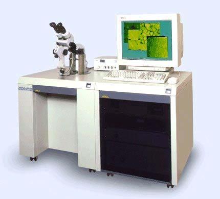
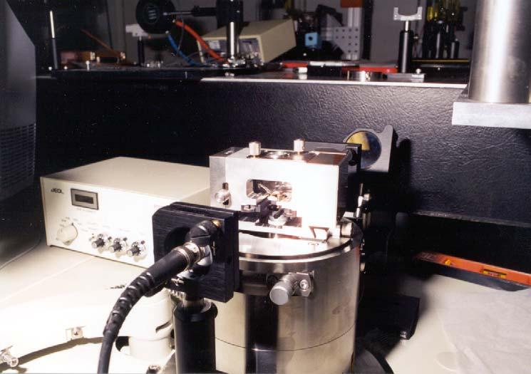
15 Scanning Near-field Infrared Microscopy
16 Extracting the Signal Lock-in Technique: The signal from the infrared detector is modulated by the resonant frequency of the cantilever (~300 khz), which is set by an external oscillator. The reference from the external oscillator is used by the lock-in to generate a sine wave that is multiplied by the signal from the IR detector. Phase Jitter (arb units) JLab FEL Drive Laser Phase Noise September 001 M. Shinn Frequency (Hz)
17 SNFIM Data MNA * /Si(100) 5140nm Trial 1 Trial In the micrographs above the images on the left are from the infrared detector. Enhanced contrast due to IR absorption is indicated by the two blue circles and the blue arrow. The fact that this experiment could be repeated is a good indication that this is truly due to IR contrast and is not an artifact of the scan. *MNA=-methyl-4nitroanaline
18 Where do we go from here? Improved optics. LN cooled InSb focal plane array for simultaneous acquisition of infrared spectra. C. A. Michaels, S. J. Stranick, L. J. Richter and R. R. Cavanagh, J. Appl. Phys. 88, 483 (000). New Laser? Wavelength modulation?
19 SNFIM Acknowledgements This work was supported by U.S. DOE Contract No. DE-AC05-84-ER40150, ONR Contract No. N , the Commonwealth of Virginia and the Laser Processing Consortium. Chuck Mooney, JEOL, USA Shin-Ichi Kitamura, JEOL, Ltd. Gwyn Williams, Jefferson Lab Kyeongwoo (Peter) Nam, NSU
The Broadband High Power THz User Facility at the Jefferson Lab - FEL
 The Broadband High Power THz User Facility at the Jefferson Lab - FEL J. Michael Klopf Jefferson Lab Core Managers Meeting June 8, 2006 Jefferson Lab Site Free Electron Laser Facility / THz Lab What is
Single Emitter Detection with Fluorescence and Extinction Spectroscopy
 Single Emitter Detection with Fluorescence and Extinction Spectroscopy Michael Krall Elements of Nanophotonics Associated Seminar Recent Progress in Nanooptics & Photonics May 07, 2009 Outline Single molecule
SNOM Challenges and Solutions
 SiO x SiO x Au Au E k SNOM Challenges and Solutions Ralf Vogelgesang, Ph.D. Ralf.Vogelgesang@fkf.mpg.de Nanoscale Science Department (Prof. Kern) Max-Planck-Institut für Festkörperforschung, Stuttgart,
Optics and Spectroscopy
 Introduction to Optics and Spectroscopy beyond the diffraction limit Chi Chen 陳祺 Research Center for Applied Science, Academia Sinica 2015Apr09 1 Light and Optics 2 Light as Wave Application 3 Electromagnetic
AFM-IR: Technology and applications in nanoscale infrared spectroscopy and chemical imaging
 Supporting Information AFM-IR: Technology and applications in nanoscale infrared spectroscopy and chemical imaging Alexandre Dazzi 1 * and Craig B. Prater 2 1 Laboratoire de Chimie Physique, Univ. Paris-Sud,
Morphology-dependent resonance induced by two-photon excitation in a micro-sphere trapped by a femtosecond pulsed laser
 Morphology-dependent resonance induced by two-photon excitation in a micro-sphere trapped by a femtosecond pulsed laser Dru Morrish, Xiaosong Gan and Min Gu Centre for Micro-Photonics, School of Biophysical
STM: Scanning Tunneling Microscope
 STM: Scanning Tunneling Microscope Basic idea STM working principle Schematic representation of the sample-tip tunnel barrier Assume tip and sample described by two infinite plate electrodes Φ t +Φ s =
Energy transport in metal nanoparticle plasmon waveguides
 Energy transport in metal nanoparticle plasmon waveguides Stefan A. Maier, Pieter G. Kik, and Harry A. Atwater California Institute of Technology Thomas J. Watson Laboratory of Applied Physics, Pasadena,
Introduction to Scanning Probe Microscopy Zhe Fei
 Introduction to Scanning Probe Microscopy Zhe Fei Phys 590B, Apr. 2019 1 Outline Part 1 SPM Overview Part 2 Scanning tunneling microscopy Part 3 Atomic force microscopy Part 4 Electric & Magnetic force
Module 26: Atomic Force Microscopy. Lecture 40: Atomic Force Microscopy 3: Additional Modes of AFM
 Module 26: Atomic Force Microscopy Lecture 40: Atomic Force Microscopy 3: Additional Modes of AFM 1 The AFM apart from generating the information about the topography of the sample features can be used
Near-Infrared Spectroscopy of Nitride Heterostructures EMILY FINAN ADVISOR: DR. OANA MALIS PURDUE UNIVERSITY REU PROGRAM AUGUST 2, 2012
 Near-Infrared Spectroscopy of Nitride Heterostructures EMILY FINAN ADVISOR: DR. OANA MALIS PURDUE UNIVERSITY REU PROGRAM AUGUST 2, 2012 Introduction Experimental Condensed Matter Research Study of large
Nanophysics: Main trends
 Nano-opto-electronics Nanophysics: Main trends Nanomechanics Main issues Light interaction with small structures Molecules Nanoparticles (semiconductor and metallic) Microparticles Photonic crystals Nanoplasmonics
Two-photon single-beam particle trapping of active micro-spheres
 Two-photon single-beam particle trapping of active micro-spheres Dru Morrish, Xiaosong Gan and Min Gu * Centre for Mirco-Photonics, School of Biophysical Sciences and Electrical Engineering, Swinburne
Scattering-type near-field microscopy for nanoscale optical imaging
 Scattering-type near-field microscopy for nanoscale optical imaging Rainer Hillenbrand Nano-Photonics Group Max-Planck-Institut für Biochemie 82152 Martinsried, Germany Infrared light enables label-free
Advanced techniques Local probes, SNOM
 Advanced techniques Local probes, SNOM Principle Probe the near field electromagnetic field with a local probe near field probe propagating field evanescent Advanced techniques Local probes, SNOM Principle
Light Interaction with Small Structures
 Light Interaction with Small Structures Molecules Light scattering due to harmonically driven dipole oscillator Nanoparticles Insulators Rayleigh Scattering (blue sky) Semiconductors...Resonance absorption
Mat. Res. Soc. Symp. Proc. 406, (1996).
.") IMAGING OF SILICON CARRIER DYNAMICS WITH NEAR-FIELD SCANNING OPTICAL MICROSCOPY A.H. LA ROSA, B.I. YAKOBSON, and H.D. HALLEN Department of Physics, North Carolina State University, Raleigh, NC 27695. ABSTRACT
IMAGING OF SILICON CARRIER DYNAMICS WITH NEAR-FIELD SCANNING OPTICAL MICROSCOPY A.H. LA ROSA, B.I. YAKOBSON, and H.D. HALLEN Department of Physics, North Carolina State University, Raleigh, NC 27695. ABSTRACT
Photonic nanojet enhancement of backscattering of light by nanoparticles: a potential novel visible-light ultramicroscopy technique
 Photonic nanojet enhancement of backscattering of light by nanoparticles: a potential novel visible-light ultramicroscopy technique Zhigang Chen and Allen Taflove Department of Electrical and Computer
Atomic and molecular interactions. Scanning probe microscopy.
 Atomic and molecular interactions. Scanning probe microscopy. Balázs Kiss Nanobiotechnology and Single Molecule Research Group, Department of Biophysics and Radiation Biology 27. November 2013. 2 Atomic
Supplementary Information for. Vibrational Spectroscopy at Electrolyte Electrode Interfaces with Graphene Gratings
 Supplementary Information for Vibrational Spectroscopy at Electrolyte Electrode Interfaces with Graphene Gratings Supplementary Figure 1. Simulated from pristine graphene gratings at different Fermi energy
Terahertz imaging using the Jefferson Lab - FEL high power broadband terahertz source
 Terahertz imaging using the Jefferson Lab - FEL high power broadband terahertz source J. Michael Klopf a), Matthew Coppinger b), Nathan Sustersic b), James Kolodzey b), and Gwyn P. Williams a) a) Jefferson
Bringing optics into the nanoscale a double-scanner AFM brings advanced optical experiments within reach
 Bringing optics into the nanoscale a double-scanner AFM brings advanced optical experiments within reach Beyond the diffraction limit The resolution of optical microscopy is generally limited by the diffraction
Nanomaterials and their Optical Applications
 Nanomaterials and their Optical Applications Winter Semester 2012 Lecture 04 rachel.grange@uni-jena.de http://www.iap.uni-jena.de/multiphoton Lecture 4: outline 2 Characterization of nanomaterials SEM,
Lecture 4 Scanning Probe Microscopy (SPM)
") Lecture 4 Scanning Probe Microscopy (SPM) General components of SPM; Tip --- the probe; Cantilever --- the indicator of the tip; Tip-sample interaction --- the feedback system; Scanner --- piezoelectric
Lecture 4 Scanning Probe Microscopy (SPM) General components of SPM; Tip --- the probe; Cantilever --- the indicator of the tip; Tip-sample interaction --- the feedback system; Scanner --- piezoelectric
SOFT X-RAYS AND EXTREME ULTRAVIOLET RADIATION
 SOFT X-RAYS AND EXTREME ULTRAVIOLET RADIATION Principles and Applications DAVID ATTWOOD UNIVERSITY OF CALIFORNIA, BERKELEY AND LAWRENCE BERKELEY NATIONAL LABORATORY CAMBRIDGE UNIVERSITY PRESS Contents
Polarization control and sensing with two-dimensional coupled photonic crystal microcavity arrays. Hatice Altug * and Jelena Vučković
 Polarization control and sensing with two-dimensional coupled photonic crystal microcavity arrays Hatice Altug * and Jelena Vučković Edward L. Ginzton Laboratory, Stanford University, Stanford, CA 94305-4088
Terahertz sensing and imaging based on carbon nanotubes:
 Terahertz sensing and imaging based on carbon nanotubes: Frequency-selective detection and near-field imaging Yukio Kawano RIKEN, JST PRESTO ykawano@riken.jp http://www.riken.jp/lab-www/adv_device/kawano/index.html
THz experiments at the UCSB FELs and the THz Science and Technology Network.
 THz experiments at the UCSB FELs and the THz Science and Technology Network. Mark Sherwin UCSB Physics Department and Institute for Quantum and Complex Dynamics UCSB Center for Terahertz Science and Technology
Other SPM Techniques. Scanning Probe Microscopy HT10
 Other SPM Techniques Scanning Near-Field Optical Microscopy (SNOM) Scanning Capacitance Microscopy (SCM) Scanning Spreading Resistance Microscopy (SSRM) Multiprobe techniques Electrostatic Force Microscopy,
Near field radiative heat transfer between a sphere and a substrate
 Near field radiative heat transfer between a sphere and a substrate Arvind Narayanaswamy Department of Mechanical Engineering, Columbia University, New York, NY 10027. Sheng Shen and Gang Chen Department
Scanning Probe Microscopy. Amanda MacMillan, Emmy Gebremichael, & John Shamblin Chem 243: Instrumental Analysis Dr. Robert Corn March 10, 2010
 Scanning Probe Microscopy Amanda MacMillan, Emmy Gebremichael, & John Shamblin Chem 243: Instrumental Analysis Dr. Robert Corn March 10, 2010 Scanning Probe Microscopy High-Resolution Surface Analysis
PC Laboratory Raman Spectroscopy
 PC Laboratory Raman Spectroscopy Schedule: Week of September 5-9: Student presentations Week of September 19-23:Student experiments Learning goals: (1) Hands-on experience with setting up a spectrometer.
nano-ftir: Material Characterization with Nanoscale Spatial Resolution
 neaspec presents: neasnom microscope nano-ftir: Material Characterization with Nanoscale Spatial Resolution AMC Workshop 2017 6th of June Dr. 2017 Tobias Gokus Company neaspec GmbH leading experts of nanoscale
Supporting Information
 Supporting Information Three-dimensional frameworks of cubic (NH 4 ) 5 Ga 4 SbS 10, (NH 4 ) 4 Ga 4 SbS 9 (OH) H 2 O, and (NH 4 ) 3 Ga 4 SbS 9 (OH 2 ) 2H 2 O. Joshua L. Mertz, Nan Ding, and Mercouri G.
requency generation spectroscopy Rahul N
 requency generation spectroscopy Rahul N 2-11-2013 Sum frequency generation spectroscopy Sum frequency generation spectroscopy (SFG) is a technique used to analyze surfaces and interfaces. SFG was first
Imaging Methods: Scanning Force Microscopy (SFM / AFM)
") Imaging Methods: Scanning Force Microscopy (SFM / AFM) The atomic force microscope (AFM) probes the surface of a sample with a sharp tip, a couple of microns long and often less than 100 Å in diameter.
Imaging Methods: Scanning Force Microscopy (SFM / AFM) The atomic force microscope (AFM) probes the surface of a sample with a sharp tip, a couple of microns long and often less than 100 Å in diameter.
Micromechanical Instruments for Ferromagnetic Measurements
 Micromechanical Instruments for Ferromagnetic Measurements John Moreland NIST 325 Broadway, Boulder, CO, 80305 Phone:+1-303-497-3641 FAX: +1-303-497-3725 E-mail: moreland@boulder.nist.gov Presented at
Spectroscopy at nanometer scale
 Spectroscopy at nanometer scale 1. Physics of the spectroscopies 2. Spectroscopies for the bulk materials 3. Experimental setups for the spectroscopies 4. Physics and Chemistry of nanomaterials Various
High-power Cryogenic Yb:YAG Lasers and Optical Particle Targeting for EUV Sources *
 High-power Cryogenic Yb:YAG Lasers and Optical Particle Targeting for EUV Sources * J.D. Hybl**, T.Y. Fan, W.D. Herzog, T.H. Jeys, D.J.Ripin, and A. Sanchez EUV Source Workshop 29 May 2009 * This work
Development of measurement technique to evaluate thermal conductivity of thermoelectric Bi 2 Te 3 submicron thin films by photothermal radiometry
 Development of measurement technique to evaluate thermal conductivity of thermoelectric Bi Te 3 submicron thin films by photothermal radiometry H Jitsukawa 1 and Y Nagasaka 1 School of Integrated Design
Free Electron Laser. Project report: Synchrotron radiation. Sadaf Jamil Rana
 Free Electron Laser Project report: Synchrotron radiation By Sadaf Jamil Rana History of Free-Electron Laser (FEL) The FEL is the result of many years of theoretical and experimental work on the generation
SPIN MICROSCOPE BASED ON OPTICALLY DETECTED MAGNETIC RESONANCE
 SPIN MICROSCOPE BASED ON OPTICALLY DETECTED MAGNETIC RESONANCE Boris M. Chernobrod and Gennady P. Berman Theoretical Division, Los Alamos National Laboratory, Los Alamos, NM 87545 Abstract We propose a
Nanoscale confinement of photon and electron
 Nanoscale confinement of photon and electron Photons can be confined via: Planar waveguides or microcavities (2 d) Optical fibers (1 d) Micro/nano spheres (0 d) Electrons can be confined via: Quantum well
Vibrational Spectroscopies. C-874 University of Delaware
 Vibrational Spectroscopies C-874 University of Delaware Vibrational Spectroscopies..everything that living things do can be understood in terms of the jigglings and wigglings of atoms.. R. P. Feymann Vibrational
Combining High Resolution Optical and Scanning Probe Microscopy
 Combining High Resolution Optical and Scanning Probe Microscopy Fernando Vargas WITec, Ulm, Germany www.witec.de Company Background Foundation 1997 by O. Hollricher, J. Koenen, K. Weishaupt WITec = Wissenschaftliche
THREE MAIN LIGHT MATTER INTERRACTION
 Chapters: 3and 4 THREE MAIN LIGHT MATTER INTERRACTION Absorption: converts radiative energy into internal energy Emission: converts internal energy into radiative energy Scattering; Radiative energy is
LIGHT CONTROLLED PHOTON TUNNELING. University of Maryland, College Park, MD Phone: , Fax: ,
 LIGHT CONTROLLED PHOTON TUNNELING Igor I. Smolyaninov 1), Anatoliy V. Zayats 2), and Christopher C. Davis 1) 1) Department of Electrical and Computer Engineering University of Maryland, College Park, MD
ECE 484 Semiconductor Lasers
 ECE 484 Semiconductor Lasers Dr. Lukas Chrostowski Department of Electrical and Computer Engineering University of British Columbia January, 2013 Module Learning Objectives: Understand the importance of
Investigation of Coherent Emission from the NSLS VUV Ring
 SPIE Accelerator Based Infrared Sources and Spectroscopic Applications Proc. 3775, 88 94 (1999) Investigation of Coherent Emission from the NSLS VUV Ring G.L. Carr, R.P.S.M. Lobo, J.D. LaVeigne, D.H. Reitze,
CHARACTERIZATION of NANOMATERIALS KHP
 CHARACTERIZATION of NANOMATERIALS Overview of the most common nanocharacterization techniques MAIN CHARACTERIZATION TECHNIQUES: 1.Transmission Electron Microscope (TEM) 2. Scanning Electron Microscope
Effect of Spiral Microwave Antenna Configuration on the Production of Nano-crystalline Film by Chemical Sputtering in ECR Plasma
 THE HARRIS SCIENCE REVIEW OF DOSHISHA UNIVERSITY, VOL. 56, No. 1 April 2015 Effect of Spiral Microwave Antenna Configuration on the Production of Nano-crystalline Film by Chemical Sputtering in ECR Plasma
Spring 2009 EE 710: Nanoscience and Engineering
 Spring 009 EE 710: Nanoscience and Engineering Part 10: Surface Plasmons in Metals Images and figures supplied from Hornyak, Dutta, Tibbals, and Rao, Introduction to Nanoscience, CRC Press Boca Raton,
l* = 109 nm Glycerol Clean Water Glycerol l = 108 nm Wavelength (nm)
") 1/ (rad -1 ) Normalized extinction a Clean 0.8 Water l* = 109 nm 0.6 Glycerol b 2.0 1.5 500 600 700 800 900 Clean Water 0.5 Glycerol l = 108 nm 630 660 690 720 750 Supplementary Figure 1. Refractive index
1/ (rad -1 ) Normalized extinction a Clean 0.8 Water l* = 109 nm 0.6 Glycerol b 2.0 1.5 500 600 700 800 900 Clean Water 0.5 Glycerol l = 108 nm 630 660 690 720 750 Supplementary Figure 1. Refractive index
Lecture 10: Surface Plasmon Excitation. 5 nm
 Excitation Lecture 10: Surface Plasmon Excitation 5 nm Summary The dispersion relation for surface plasmons Useful for describing plasmon excitation & propagation This lecture: p sp Coupling light to surface
The effects of probe boundary conditions and propagation on nano- Raman spectroscopy
 The effects of probe boundary conditions and propagation on nano- Raman spectroscopy H. D. Hallen,* E. J. Ayars** and C. L. Jahncke*** * Physics Department, North Carolina State University, Raleigh, NC
Ultrafast All-optical Switches Based on Intersubband Transitions in GaN/AlN Multiple Quantum Wells for Tb/s Operation
 Ultrafast All-optical Switches Based on Intersubband Transitions in GaN/AlN Multiple Quantum Wells for Tb/s Operation Jahan M. Dawlaty, Farhan Rana and William J. Schaff Department of Electrical and Computer
A tutorial on meta-materials and THz technology
 p.1/49 A tutorial on meta-materials and THz technology Thomas Feurer thomas.feurer@iap.unibe.ch Institute of Applied Physics Sidlerstr. 5, 3012 Bern Switzerland p.2/49 Outline Meta-materials Super-lenses
Understanding Nanoplasmonics. Greg Sun University of Massachusetts Boston
 Understanding Nanoplasmonics Greg Sun University of Massachusetts Boston Nanoplasmonics Space 100pm 1nm 10nm 100nm 1μm 10μm 100μm 1ns 100ps 10ps Photonics 1ps 100fs 10fs 1fs Time Surface Plasmons Surface
Highly Efficient and Anomalous Charge Transfer in van der Waals Trilayer Semiconductors
 Highly Efficient and Anomalous Charge Transfer in van der Waals Trilayer Semiconductors Frank Ceballos 1, Ming-Gang Ju 2 Samuel D. Lane 1, Xiao Cheng Zeng 2 & Hui Zhao 1 1 Department of Physics and Astronomy,
Analysis of Thermal Diffusivity of Metals using Lock-in Thermography
 Analysis of Thermal Diffusivity of Metals using Lock-in Thermography by F. Wagner*, T. Malvisalo*, P. W. Nolte**, and S. Schweizer** * Department of Electrical Engineering, South Westphalia University
Nano-optics. Topics: How do we image things on the nanoscale? How do we use nanofabrication for new optical devices? COSMOS 2006 Lecture 1
 Nano-optics Topics: How do we image things on the nanoscale? How do we use nanofabrication for new optical devices? Wave Optics 1. Electromagnetic wave x Ex λ Direction of Propagation y z z plane wave
High-power Cryogenic Yb:YAG Lasers and Optical Particle Targeting for EUV Sources *
 High-power Cryogenic Yb:YAG Lasers and Optical Particle Targeting for EUV Sources * J.D. Hybl**, T.Y. Fan, W.D. Herzog, T.H. Jeys, D.J.Ripin, and A. Sanchez 2008 International Workshop on EUV Lithography
Near-field optical imaging of noble metal nanoparticles
 Eur. Phys. J. Appl. Phys. 28, 3 18 (2004) DOI: 10.1051/epjap:2004170 THE EUROPEAN PHYSICAL JOURNAL APPLIED PHYSICS Near-field optical imaging of noble metal nanoparticles G.P. Wiederrecht a Chemistry Division
Widely Tunable and Intense Mid-Infrared PL Emission from Epitaxial Pb(Sr)Te Quantum Dots in a CdTe Matrix
Te Quantum Dots in a CdTe Matrix") Widely Tunable and Intense Mid-Infrared PL Emission from Epitaxial Pb(Sr)Te Quantum Dots in a Matrix S. Kriechbaumer 1, T. Schwarzl 1, H. Groiss 1, W. Heiss 1, F. Schäffler 1,T. Wojtowicz 2, K. Koike 3,
Widely Tunable and Intense Mid-Infrared PL Emission from Epitaxial Pb(Sr)Te Quantum Dots in a Matrix S. Kriechbaumer 1, T. Schwarzl 1, H. Groiss 1, W. Heiss 1, F. Schäffler 1,T. Wojtowicz 2, K. Koike 3,
Supplementary Figure 1: Experimental measurement of polarization-dependent absorption properties in all-fibre graphene devices. a.
 Supplementary Figure 1: Experimental measurement of polarization-dependent absorption properties in all-fibre graphene devices. a. Schematic of experimental set-up including an amplified spontaneous emission
Graphene Based Saturable Absorber Modelockers at 2µm
 ISLA Workshop Munich Integrated disruptive components for 2µm fibre Lasers ISLA Graphene Based Saturable Absorber Modelockers at 2µm Prof. Werner Blau - Trinity College Dublin Friday, 26th of June 2015
Survey on Laser Spectroscopic Techniques for Condensed Matter
 Survey on Laser Spectroscopic Techniques for Condensed Matter Coherent Radiation Sources for Small Laboratories CW: Tunability: IR Visible Linewidth: 1 Hz Power: μw 10W Pulsed: Tunabality: THz Soft X-ray
LASER-COMPTON SCATTERING AS A POTENTIAL BRIGHT X-RAY SOURCE
 Copyright(C)JCPDS-International Centre for Diffraction Data 2003, Advances in X-ray Analysis, Vol.46 74 ISSN 1097-0002 LASER-COMPTON SCATTERING AS A POTENTIAL BRIGHT X-RAY SOURCE K. Chouffani 1, D. Wells
Signal regeneration - optical amplifiers
 Signal regeneration - optical amplifiers In any atom or solid, the state of the electrons can change by: 1) Stimulated absorption - in the presence of a light wave, a photon is absorbed, the electron is
Introduction to Microeletromechanical Systems (MEMS) Lecture 9 Topics. MEMS Overview
 Lecture 9 Topics. MEMS Overview") Introduction to Microeletromechanical Systems (MEMS) Lecture 9 Topics MicroOptoElectroMechanical Systems (MOEMS) Grating Light Valves Corner Cube Reflector (CCR) MEMS Light Modulator Optical Switch Micromirrors
Introduction to Microeletromechanical Systems (MEMS) Lecture 9 Topics MicroOptoElectroMechanical Systems (MOEMS) Grating Light Valves Corner Cube Reflector (CCR) MEMS Light Modulator Optical Switch Micromirrors
The Scattering of Light by Small Particles. Advanced Laboratory, Physics 407 University of Wisconsin Madison, Wisconsin 53706
 (4/6/10) The Scattering of Light by Small Particles Advanced Laboratory, Physics 407 University of Wisconsin Madison, Wisconsin 53706 Abstract In this experiment we study the scattering of light from various
An infrared photon scanning tunnelling microscope for investigations of near-field imaging
 J. Opt. A: Pure Appl. Opt. 1 (1999) 517 522. Printed in the UK PII: S1464-4258(99)03568-0 An infrared photon scanning tunnelling microscope for investigations of near-field imaging J C Quartel and J C
Ultra-Slow Light Propagation in Room Temperature Solids. Robert W. Boyd
 Ultra-Slow Light Propagation in Room Temperature Solids Robert W. Boyd The Institute of Optics and Department of Physics and Astronomy University of Rochester, Rochester, NY USA http://www.optics.rochester.edu
SUPPLEMENTARY FIGURES
 SUPPLEMENTARY FIGURES Supplementary Figure 1. Projected band structures for different coupling strengths. (a) The non-dispersive quasi-energy diagrams and (b) projected band structures for constant coupling
Nanoscale Chemical Imaging with Photo-induced Force Microscopy
 OG2 BCP39nm_0062 PiFM (LIA1R)Fwd 500 279.1 µv 375 250 nm 500 375 250 125 0 nm 125 219.0 µv Nanoscale Chemical Imaging with Photo-induced Force Microscopy 0 Thomas R. Albrecht, Derek Nowak, Will Morrison,
Imaging Methods: Breath Patterns
 Imaging Methods: Breath Patterns Breath / condensation pattern: By cooling a substrate below the condensation temperature H 2 O will condense in different rates on the substrate with the nucleation rate
The Scattering of Light by Small Particles. Advanced Laboratory, Physics 407 University of Wisconsin Madison, Wisconsin 53706
 (4/28/09) The Scattering of Light by Small Particles Advanced Laboratory, Physics 407 University of Wisconsin Madison, Wisconsin 53706 Abstract In this experiment we study the scattering of light from
Study of polarization-dependent energy coupling between near-field optical probe and mesoscopic metal structure
 JOURNAL OF APPLIED PHYSICS VOLUME 95, NUMBER 8 15 APRIL 2004 Study of polarization-dependent energy coupling between near-field optical probe and mesoscopic metal structure A. Gademann and I. V. Shvets
Multi-cycle THz pulse generation in poled lithium niobate crystals
 Laser Focus World April 2005 issue (pp. 67-72). Multi-cycle THz pulse generation in poled lithium niobate crystals Yun-Shik Lee and Theodore B. Norris Yun-Shik Lee is an assistant professor of physics
Laser-synthesized oxide-passivated bright Si quantum dots for bioimaging
 Supplementary Information to Laser-synthesized oxide-passivated bright Si quantum dots for bioimaging M. B. Gongalsky 1, L.A. Osminkina 1,2, A. Pereira 3, A. A. Manankov 1, A. A. Fedorenko 1, A. N. Vasiliev
2001 Spectrometers. Instrument Machinery. Movies from this presentation can be access at
 2001 Spectrometers Instrument Machinery Movies from this presentation can be access at http://www.shsu.edu/~chm_tgc/sounds/sound.html Chp20: 1 Optical Instruments Instrument Components Components of various
Simple strategy for enhancing terahertz emission from coherent longitudinal optical phonons using undoped GaAs/n-type GaAs epitaxial layer structures
 Presented at ISCS21 June 4, 21 Session # FrP3 Simple strategy for enhancing terahertz emission from coherent longitudinal optical phonons using undoped GaAs/n-type GaAs epitaxial layer structures Hideo
Resolving near-field from high order signals of scattering near-field scanning optical microscopy
 Resolving near-field from high order signals of scattering near-field scanning optical microscopy Nan Zhou, Yan Li, and Xianfan Xu * School of Mechanical Engineering and Birck Nanotechnology Center, Purdue
Laser Basics. What happens when light (or photon) interact with a matter? Assume photon energy is compatible with energy transition levels.
 interact with a matter? Assume photon energy is compatible with energy transition levels.") What happens when light (or photon) interact with a matter? Assume photon energy is compatible with energy transition levels. Electron energy levels in an hydrogen atom n=5 n=4 - + n=3 n=2 13.6 = [ev]
What happens when light (or photon) interact with a matter? Assume photon energy is compatible with energy transition levels. Electron energy levels in an hydrogen atom n=5 n=4 - + n=3 n=2 13.6 = [ev]
Segmented 1.55um Laser with 400% Differential Quantum Efficiency J. Getty, E. Skogen, L. Coldren, University of California, Santa Barbara, CA.
 Segmented 1.55um Laser with 400% Differential Quantum Efficiency J. Getty, E. Skogen, L. Coldren, University of California, Santa Barbara, CA. Abstract: By electrically segmenting, and series-connecting
SUPPLEMENTARY INFORMATION
 1. Supplementary Methods Characterization of AFM resolution We employed amplitude-modulation AFM in non-contact mode to characterize the topography of the graphene samples. The measurements were performed
Raman spectroscopy study of rotated double-layer graphene: misorientation angle dependence of electronic structure
 Supplementary Material for Raman spectroscopy study of rotated double-layer graphene: misorientation angle dependence of electronic structure Kwanpyo Kim 1,2,3, Sinisa Coh 1,3, Liang Z. Tan 1,3, William
Studies of the Spin Dynamics of Charge Carriers in Semiconductors and their Interfaces. S. K. Singh, T. V. Shahbazyan, I. E. Perakis and N. H.
 Studies of the Spin Dynamics of Charge Carriers in Semiconductors and their Interfaces S. K. Singh, T. V. Shahbazyan, I. E. Perakis and N. H. Tolk Department of Physics and Astronomy Vanderbilt University,
Surface Plasmon Amplification by Stimulated Emission of Radiation. By: Jonathan Massey-Allard Graham Zell Justin Lau
 Surface Plasmon Amplification by Stimulated Emission of Radiation By: Jonathan Massey-Allard Graham Zell Justin Lau Surface Plasmons (SPs) Quanta of electron oscillations in a plasma. o Electron gas in
Observation of coupled plasmon-polariton modes of plasmon waveguides for electromagnetic energy transport below the diffraction limit
 Mat. Res. Soc. Symp. Proc. Vol. 722 2002 Materials Research Society Observation of coupled plasmon-polariton modes of plasmon waveguides for electromagnetic energy transport below the diffraction limit
Vibrational Spectroscopy of Molecules on Surfaces
 Vibrational Spectroscopy of Molecules on Surfaces Edited by John T. Yates, Jr. University of Pittsburgh Pittsburgh, Pennsylvania and Theodore E. Madey National Bureau of Standards Gaithersburg, Maryland
Clark Atlanta University Center for Surface Chemistry and Catalysis Instrument Capabilities
 Center for Surface Chemistry and Catalysis Instrument Capabilities For information contact: Dr. Eric Mintz Research Center for Science and Technology Clark Atlanta University Atlanta, Georgia 30314 Phone:
Superconductivity Induced Transparency
 Superconductivity Induced Transparency Coskun Kocabas In this paper I will discuss the effect of the superconducting phase transition on the optical properties of the superconductors. Firstly I will give
Spatial Coherence Properties of Organic Molecules Coupled to Plasmonic Surface Lattice Resonances in the Weak and Strong Coupling Regimes
 Spatial Coherence Properties of Organic Molecules Coupled to Plasmonic Surface Lattice Resonances in the Weak and Strong Coupling Regimes Supplemental Material L. Shi, T. K. Hakala, H. T. Rekola, J. -P.
HYPER-RAYLEIGH SCATTERING AND SURFACE-ENHANCED RAMAN SCATTERING STUDIES OF PLATINUM NANOPARTICLE SUSPENSIONS
 www.arpapress.com/volumes/vol19issue1/ijrras_19_1_06.pdf HYPER-RAYLEIGH SCATTERING AND SURFACE-ENHANCED RAMAN SCATTERING STUDIES OF PLATINUM NANOPARTICLE SUSPENSIONS M. Eslamifar Physics Department, BehbahanKhatamAl-Anbia
Development of a compact Yb optical lattice clock
 Development of a compact Yb optical lattice clock A. A. Görlitz, C. Abou-Jaoudeh, C. Bruni, B. I. Ernsting, A. Nevsky, S. Schiller C. ESA Workshop on Optical Atomic Clocks D. Frascati, 14 th 16 th of October
Improving nano-scale imaging of of intergrated micro-raman/afm systems using negativestiffness
 See vibration isolation technology @ www.minusk.com?pdf) Electronic Products and Technology - May 2014 Improving nano-scale imaging of of intergrated micro-raman/afm systems using negativestiffness vibration
Plasmonics: elementary excitation of a plasma (gas of free charges) nano-scale optics done with plasmons at metal interfaces
 nano-scale optics done with plasmons at metal interfaces") Plasmonics Plasmon: Plasmonics: elementary excitation of a plasma (gas of free charges) nano-scale optics done with plasmons at metal interfaces Femius Koenderink Center for Nanophotonics AMOLF, Amsterdam
Plasmonics Plasmon: Plasmonics: elementary excitation of a plasma (gas of free charges) nano-scale optics done with plasmons at metal interfaces Femius Koenderink Center for Nanophotonics AMOLF, Amsterdam
SUPPLEMENTARY INFORMATION
 SUPPLEMENTARY INFORMATION Supplementary Information I. Schematic representation of the zero- n superlattices Schematic representation of a superlattice with 3 superperiods is shown in Fig. S1. The superlattice
Visualization of Xe and Sn Atoms Generated from Laser-Produced Plasma for EUV Light Source
 3rd International EUVL Symposium NOVEMBER 1-4, 2004 Miyazaki, Japan Visualization of Xe and Sn Atoms Generated from Laser-Produced Plasma for EUV Light Source H. Tanaka, A. Matsumoto, K. Akinaga, A. Takahashi