Organic LEDs: Today displays, lighting tomorrow? Lieven Penninck, Stephane Altazin, Beat Ruhstaller , summer school, Belgium
|
|
|
- Dora York
- 6 years ago
- Views:
Transcription


1 Organic LEDs: Today displays, lighting tomorrow? Lieven Penninck, Stephane Altazin, Beat Ruhstaller , summer school, Belgium
2 Content OLED applications & back ground Operation principles From charge to photon Light extraction Conclusion


3 Simulation Software Measurement Hardware Who we are Research on OLED and OPV


4 Setfos 4.1 Software Modules:


5 All-in-One!


6 Fluxim Distribution partners: Research partners:


7 Fluxim s team Distribution partners: Research partners:
8 Content OLED applications & background Operation principles From charge to photon Light extraction Conclusion


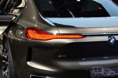
9 rganic and Large Area Electronics & Photovoltaics OLED lamps Lumiblade by Philips Tridonic, Austria 55 inch OLED TV from LG, Korea OLED flexible display, Samsung, Korea Organic solar cells by Konarka, USA


10 OLED displays


11 OLED vs. LCD display

 Efficient")
12 OLED lighting High CRI & warm white Dimmable Large area (not blinding) Efficient Flexible/shatterproof/transparent? Low production cost (roll to roll)


13 OLED vs. other lighting


14 OLED: lighting 14

15 Organic LEDs NOT small size lab sample Panasonic SID

16 OPV: organic photovoltaics Low cost ~ less efficient than conventional PV Flexible Free form shapes Organic solar cells by Konarka, USA
17 OLED: structure Cathode ETL HBL EML EBL Organic semiconductor + metal/ito electrodes Stack of thin layers (total ~200nm) HTL Anode Glass/PET/Steel Electron/hole transport, emitting layers Deposited by evaporation/ spinning/ printing,... - V + Cathode ETL HBL EML EBL HTL Anode Substrate 17
18 OLED Aluminium/ Silver ETL HBL EML EBL HTL ITO Substrate Bottom emission Thick metal=mirror Al/Ag >100nm Transparent anode ITO/ PEDOT Top emission Aluminium/Silver ETL HBL EML EBL HTL Aluminium/Silver Substrate Thin metal=(semi-) transparent Al/Ag ~20nm Thick metal=mirror Al/Ag >100nm 18


19 Aluminium/ Silver ETL R G B HTL ITO Substrate


20 Aluminium/ Silver ETL R HTL CGL ETL G HTL CGL ETL B HTL ITO Substrate


21

22


")

23 OLED Challenges Optimize EQE, Color... Monitor & understand Design panels/displays, Minimize losses Extract charge mobility Nowy et al. JAP (2010) C(f) for fresh & aged OLED Simulated potential with metal grid & shunts
24 Content OLED applications & back ground Operating principles From charge to photon Light extraction Conclusion
25 OLED: basic principle Cathode ETL - EBL EML - HBL HTL Anode Electron/hole injection Charge transport LUMO Recombination Light emission HOMO + + Light extraction 25


26 Efficiency definition EQE cb st rad out


27 lm hc LCE 683 ( ) ( ) V ( ) S0( ) d e air cb st rad out W 0 LE air LCE V air *S. Mladenovski et. al. Journal of Applied Physics 109, (2011) 28
28 Content OLED applications & back ground Operating principles From charge to photon Light extraction Conclusion


29 Organic semiconductor ETL EML HTL - - LUMO HOMO


30 Actual charge transport

 *exp 0 T")
31 Gaussian Disorder Model (GDM) ( ) *exp 0 T C kt B 2

32 - Charge balance ETL EML HTL - LUMO EQE cb st rad out HOMO


33 «Current Balance» & Recombination in OLEDs Perfect balance = all charges recombine Jrec cb J


34 Blocking layers ETL HBL EML HTL - LUMO - HOMO


35 Blocking layers 1 cb 1 cb 37

36 Electron + hole recombine Not all excitons CAN emit light Spin state: 25% singlet, 75% triplet Fluorescent emitters traditional OLED materials: AlQ 3, EQE cb st rad out Fluorescent: only singlets η st =25% 44
37 Phophorescent emitters: triplet decay ISC: Singlets-> triplets Guest/host system Ir(ppy)3, Contain Ir or Pt -> Expensive Phosphorescent emitters: triplets+singlets η st =100% EQE cb st rad out 45


38 Hot topic : TADF Thermally activated delayed fluorescence reverse ISC: triplets<->singlet IQE depends on T No Ir: high efficiency at low cost EQE cb st rad out 46


39 IQE S T 1 T S T T st IQE st rad

40 1,2 2 k k k k k k k k 4 k k k k k k 2 r T nr S r T nr S r nr nr T S r


41
42 EQE=η cb η st η rad η out * rad r r nr r [1/ µs] F tot r nr ** F=total emitted power constant Depends on microcavity rad F r r F nr *S. Mladenovski et al.; J. App. Phys. 109; (2011) **S. Mladenovski et al.; Opt. Lett. 34; (2009) 50
43 Investigating η rad : phosphorescence lifetime 1/ L Lifetime in different devices Time resolved luminescence Fit F rad ~ exp( t/ ) Mladenowski, Reineke, Neyts (2009) Penninck, Steinbacher, Krause, Neyts (2012) 51
44 Start from Drift-diffusion equations. Excitons continuity equation is then solved accounting the optical feedback (quenching & recombination). Every radiatively decaying exciton is considered as an emitting dipole in the optical model.


45
 F n N")


46 rad F r ( I) F n N r nr TPQ TTA rad rad
47 Content OLED applications & back ground Operation principles From charge to photon Light extraction Conclusion


48 EQE=η cb η st η rad η out Light emitted in all directions 2 barriers in OLED: Organic: n=1.8 Glass/plastic: n=1.5 Air n=1 η out =15-20% is outcoupled Escape cone: 56 Escape cone: 42 57


49 Ways to improve light outcoupling: OLED Stack design Outcoupling layers Oriented emitters q=1 q=0.7

50 Emission inside OLED Dipole antenna in planar 1D layer stack Interference between reflections on layer boundaries TE & TM polarization R TM RTE E TM Modified emitted field E TE E cav,te/tm E a E,TE/TM TE / TM,TE/TM 1 a TE / TM a TE / TM 60
51 Metal electrodes = mirror surface Interference increases/reduces emission for certian wavelengths & angles Distance to cathode modifies spectrum & efficiency Aluminium(100nm) ETL (varied) HBL (10nm) EML(20nm) EBL(10nm) HTL(60nm) ITO(90nm) Substrate 61


52

] / Ba(1 nm)/al (12 nm) top emission Emitted radiance well")
53 Optical Model: Validation Bottom (through glass) and top emission due to semitransparent electrodes bottom emission Device: Al(12 nm)/pedot(60 nm)/ [76% PVK+19% PBD+5% CGR-Red(x nm)] / Ba(1 nm)/al (12 nm) top emission Emitted radiance well reproduced!
54 η out (%) Air Substrate d_etl(nm) 64
55 Ways to improve light outcoupling: OLED Stack design Outcoupling layers Oriented emitters q=1 q=0.7


56 Structured layers for outcoupling: Redirect trapped light External outcoupling: from glass to air Internal outcoupling: from organic to glass & glass to air 66

57 Light extracted in many passes Competition between scattering & absorption Maximum outcoupling: -effective scattering -high reflectivity 60% trapped in organic layers Internal > external But difficult Internal & external combined 67


58 68
59 Scattering simulation workflow OLED-stack Dipole radiation Net Radiation Model Scattering Mie Theory Measurement BSDF Semi-analytical dipole emission model R & T Ray tracing Analytical scattering Full wave simulation 69


60 Design Challenges for Scattering OLEDs Scattering properties? Ideal haze? Angular width? OLED stack properties? OLED reflectivity? Absorption in OLED layers??
61 Emitted power (W.m -2 ) Impact of Haze on Emitted Power How strong should scattering be? (amount of haze?) BSDF assumed Lambertian(cos(θ)) R & T = flat case Scattering case Flat case Haze Emitted power in air increases with the Haze. Even with 50% haze the emitted power almost doubles!
62 Radiance (W.m -2.sr -1 ) Emitted power (W) Impact of the Scattering Function on the outcoupling Efficiency of a White OLED : Phong factor l = 1 : Phong factor l = 0.1 : Phong factor l = Angle a (degree) Sub- Lambertian Super- Lambertian Phong Factor l Scattering function: cos l (θ) maximum out-coupling efficiency l >1 Too broad scattering functions (l <1) has a negative impact on the outcoupling efficiency of the OLED.
 Impact of the scattering layer on")


63 Emitted power (W.m -2.nm -1 ) Impact of the scattering layer on the emitted color Haze= Increasing Haze from 0 to 1 : ref OLED (WO high index layer) Haze= Integrated emitted spectrum on the full up space


64 Colour stability vs angle Example: Ir:ppy 3 green pixel No scattering: Colour shift with angle 0-90 toward blue/cyan With scattering: Stable colour
65 Example: optimizing scattering particles Spherical particles Distributed in host material Key parameters: size concentration refractive index (host & particle) Mie theory (1 particle) Monte Carlo simulation (many particles) 75


66 Influence of scattering particles on the outcoupling

67 What size should the particles be? Varied radius nm Highest extraction: R=640nm Particle ~1 wavelength radius
68 Emitted power (W.m -2.sr -1 ) Emitted power (W.m -2 ) Impact of Layer Absorption Assumed k 10-4 of the planarization layer Scattering case 10 Thickness from 1 to 19 um Flat case Angle θ (degree) Thickness (um) Increasing thickness of absorbing layer: a decrease of emitted power changed shape of the radiance (high absorbance at large angles)


69 OLED stack reflectance Influence of OLED Stack Reflectance How does the cathode material impact the out-coupling enhancement? Aluminum, flat Silver, flat Aluminum, rough Silver, rough P-reflectance using Aluminum P-reflectance using Silver Rough internal glass interface: RMS=100 nm wavelength (nm) In the planar case, the silver electrode leads to poorer light outcoupling than aluminum. However, the scattering structure asks for a high-reflectance OLED stack, thus silver gives higher outcoupled radiance.


70 Influence of OLED Stack Reflectance λ=530nm Perfect reflector n=0 k>0 Higher reflection= better extraction


71 Keep in mind

72 Joint optimization of stack + particle concentration Enhanced brightness: factor 1,9 1 st and 2 nd maximum shift when scattering Improved angular colour stability


73 Angle Summary of Simulation Workflow (b) 90 Haze= Wavelength (nm) 0
74 Ways to improve light outcoupling: OLED Stack design Outcoupling layers Oriented emitters q=1 q=0.7
75 Emission & outcoupling in OLEDs: oriented dipoles Different radiation for different dipole orientation Horizontal (// OLED plane) radiate into escape cone Oriented emitters: high, no structures out 85
76 Organic LEDs: decay rate Al (200nm) TPBi (x nm) TPBi:Ir(MDQ) 2 (acac)/ir(ppy) 3 (5nm) TCTA (30nm) ITO (120nm) Glass Decay rate & radiative efficiency changes with optical design & dipole orientation 2 emitters in different layer stacks Measure decay rate per device Determine decay rates (& efficiency) & dipole orientation 86
77 EL Decay Phosphorescence lifetime extraction Exponential decay ~2μs
78 Emission & outcoupling in OLEDs: oriented dipoles [1/ µs] af (1 a) F tot r nr Different radiation for different dipole orientation vertical fraction Purcell effect 88
79 Organic LEDs: Outcoupling Ir(ppy) 3 Measurement vs. calculation Ir(MDQ)2 acac Random & experiment correspond 67% horizontal 33% vertical Random & experiment don t correspond Better description: 79% horizontal 21% vertical 89
80 Organic LEDs: Outcoupling Ir(MDQ) 2 acac Alternative method Angular spectrum Detect orientation in bad layer design Same α *W. Brütting et.al. U. Augsburg 90
 TPBi:Ir(MDQ) 2 (acac) (5nm) TCTA")

81 Organic LEDs: Outcoupling Al (200nm) TPBi (0-350nm) TPBi:Ir(MDQ) 2 (acac) (5nm) TCTA (30nm) ITO (120nm) Glass substrate η η air α α α=80% enhancement= α=100% enhancement=1.4 91
 TPBi (0-350nm)")
 Al (200 nm) glass")

82 Optimization: top emitting OLED Ag(15nm) TPBi (0-350nm) TPBi:Ir(MDQ) 2 (acac)(5nm) TCTA(80nm) Al (200 nm) glass η air α α α=80% enhancement=1.21 α=100% enhancement=
83 Concluding remarks OLED display & lighting High efficiency by: -high performance emitter materials -carefull layer design -outcoupling structures Future challenges: flexible (foldable, rollabel), transparent, cost


84 Acknowledgments UGent: Kristiaan Neyts, Patrick De Viscchere, Saso Mladenowski Fluxim: Felix Müller, Martin Neukom, Benjamin Perucco, et al. ZHAW: Evelyne Knapp, Thomas Lanz, Kevin Lapagna
85 Thank you for your attention! Any questions?
86 Electrical simulation: drift diffusion Case study: a red OLED


87


88


89 θ 1000 π Current_density Voltage =

90


91


92 Transient Electroluminescence Voltage EL rise decay t delay

93 OLED Transient Electroluminescence: Turnon Dynamics Time t d +t 1 is related to effecitve mobility and comparable to DIT mobility (Pinner et al. 2000) EL(t) Plot 1-EL norm (t) Plot
94 Transient Electroluminescence Application example: Transient EL for extraction of phosphorescence lifetime & emitter orientation Aging study: S1: fresh L=100 %, S2: aged L=90 %, S3: aged L=75%) Bi-exponential decay? Competing decay channel? Mladenowski, Reineke, Neyts (2009) 104
95 Setfos for OLED ransient EL experiment Transient EL simulation Simulating experiments to extract material parameters Turn-on delay Phosphorescence lifetime
96 All-in-One! Impedance Spectroscopy Transient Photocurrent Transient Photovoltage Capacitance-Voltage Photo-CELIV Dark Injection Transients IV-Curves 2.0 Transient EL 106
97 Light Solar Cell Version OLED Version - + DUT Solar Cell OLED + - Light LED Photodiode 111
98 Photo-CELIV Ligh t Voltag e Current t t Determine charge carrier mobility Determine number of free charge carriers in the device Apply voltage ramp Charge carriers are generated before (by light pulse) t 112
99 Analysis of CELIV currents Current t max n j disp Charge carrier mobility m = 2 d2 3 A t 1 2 max Dj j 0 Charge carrier density t n = 1 V t 0 ò 0 Relative el. permittivity j(t)dt e r = j disp d e 0 A 113
100 Experimental CELIV with PAIOS CELIV For characterization of photo-carrier dynamics Numerical CELIV simulation with SETFOS for parameter extraction More detailed physical description than analytical formula for charge mobility 114
101 Numerical Simulation of CELIV CELIV For characterization of photo-carrier dynamics Numerical CELIV simulation with SETFOS for parameter extraction More detailed physical description than analytical formula for charge mobility: m = 2 d2 3 A t 1 2 max Dj j 0 References: - M.T. Neukom, N.A. Reinke, K.A. Brossi, and B. Ruhstaller, Proc. SPIE, Vol. 7722, 77220V (2010) - M.T. Neukom, N.A. Reinke and B. Ruhstaller, Solar Energy (2011); - M.T. Neukom, S. Züfle, B. Ruhstaller, Organic Electronics 13 (2012)

102 Dark-CELIV Ligh t Voltag e Current t t Apply voltage ramp No charge carriers are generated before Determine charge carrier mobility Determine number of free charge carriers in the device -> Doping concentration t 116
103 Doping Extraction from dark-celiv Doping level is determined for an organic solar cell at different aging conditions.
104 Impedance Spectroscopy Voltage V V ac e Applying small oscillating voltage with frequency ω V ( t) 0 i t Current Phase t Measure current and calculate admittance Y = 1 Z = J ac V ac t Y = G+i w C Conductance Capacitance E. Knapp and B. Ruhstaller, Appl. Phys. Lett. 99, (2011) E. Knapp and B. Ruhstaller, J. Appl. Phys. (2012)

105 Aging Doping Aging study with C-f Paios Measurement Setfos Simulation Doping reproduces aging effect 119

106 PEDOT:PSS HBL & ITO Why does the capacitance increase? Hole w/ doping Depletion layer close to the ZNO interface Hole w/o doping W Increased hole density in the middle of the device Schottky-Model Electrons w/o doping W 2 q N a bi V Electrons w/ doping Capacitance increases with doping 120

107 C-V on bi-layer device Wolfgang Brütting, Uni Augsburg, 2001
108 Capacitance-Voltage C-V Capacitance Mott-Shottky 1/C 2 V peak Constant frequency varied offset voltage V peak is sensitive on barriers and V bi C geom 0 Negative capacitance due to recombination Offset- Voltage Extracting doping density (only for thick and highly doped devices)
109 OLED Degradation: Dark-injection Transients Aging study: S1: fresh L=100 %, S2: aged L=90 %, S3: aged L=75%) DIT/T-SCLC peak position (i.e. transit time) is unchanged, only the current is reduced! Charge mobility is unchanged!
110 OLED aging with C-V Capacitance C(V) aging Aging study on OLED Shifted peak indicates lowered charge injection unpublished

111 C-V simulation Geometrical capacitance SCLC capacitance - 1 2

112 Light Scattering Simulation for Si Thin Film Solar Cells T. Lanz, B. Ruhstaller, C. Battaglia, and C. Ballif, "Extended light scattering model incorporating coherence for thin-film silicon solar cells", J. Appl. Phys. 110, (2011)
113 Light-scattering in Organic Solar Cells Experiment Simulation (SETFOS) Cell with textured FTO achieves +10% photocurrent (J sc )! Qualitative agreement! Hu, Zhang, Zhao, Appl. Phys. Lett. 100, (2012); doi: /
Modeling Electronic and Excitonic Processes in OLED Devices
 Modeling Electronic and Excitonic Processes in OLED Devices Beat Ruhstaller 1,2 1 Fluxim AG, Switzerland 2 Zurich Univ. of Applied Sciences, Inst. of Computational Physics, Switzerland TADF Summer School
Enhancement of Light Outcoupling Efficiency in OLEDs
 Enhancement of Light Outcoupling Efficiency in OLEDs Stéphane Altazin*, Lidia Stepanova*, Lieven Penninck*, Christoph Kirsch**, Beat Ruhstaller** *Fluxim AG, Winterthur, Switzerland **Zurich University
Light Extraction in OLED with Corrugated Substrates Franky So
 Light Extraction in OLED with Corrugated Substrates Franky So Department of Materials Science and Engineering North Carolina State University Raleigh, NC 27695-7907 1 Where Did the Light Go? Modes Distribution
Organic Device Simulation Using Silvaco Software. Silvaco Taiwan September 2005
 Organic Device Simulation Using Silvaco Software Silvaco Taiwan September 2005 Organic Devices Simulation: Contents Introduction Silvaco TCAD Simulator Theory Models OTFT Simulation v.s Measurement OLED
We are IntechOpen, the world s leading publisher of Open Access books Built by scientists, for scientists. International authors and editors
 We are IntechOpen, the world s leading publisher of Open Access books Built by scientists, for scientists 3,9 116, 12M Open access books available International authors and editors Downloads Our authors
Advanced Simulation Methods for Charge Transport in OLEDs
 FLUXiM Advanced Simulation Methods for Charge Transport in OLEDs Evelyne Knapp, B. Ruhstaller Overview 1. Introduction 2. Physical Models 3. Numerical Methods 4. Outlook www.icp.zhaw.ch ICP Team Interdisciplinary
How does a polymer LED OPERATE?
 How does a polymer LED OPERATE? Now that we have covered many basic issues we can try and put together a few concepts as they appear in a working device. We start with an LED:. Charge injection a. Hole
Making OLEDs efficient
 Making OLEDs efficient cathode anode light-emitting layer η = γ EL r ηpl k st External Efficiency Outcoupling Internal efficiency of LEDs η = γ EL r ηpl k st γ = excitons formed per charge flowing in the
Flexible Organic Photovoltaics Employ laser produced metal nanoparticles into the absorption layer 1. An Introduction
 Flexible Organic Photovoltaics Employ laser produced metal nanoparticles into the absorption layer 1. An Introduction Among the renewable energy sources that are called to satisfy the continuously increased
Mesoporous titanium dioxide electrolyte bulk heterojunction
 Mesoporous titanium dioxide electrolyte bulk heterojunction The term "bulk heterojunction" is used to describe a heterojunction composed of two different materials acting as electron- and a hole- transporters,
λ = 550 nm n org = 1.8 High-index layer (n H d H = λ/4) Glass for n H =λ/4 (nm) d H Calculated EQE (%) (%) d org : 150 nm
 Glass for n H =λ/4 (nm) d H Calculated EQE (%) (%) d org : 150 nm") a Al d dipole : 70 nm from Al Emitter : Ir(ppy) 2 acac n org = 1.8 R bot d org : 150 nm 4-layer graphene High-index layer (n H d H = λ/4) Glass R bot (%) b 40 35 30 25 20 15 10 5 0 d H for n H d H =λ/4
a Al d dipole : 70 nm from Al Emitter : Ir(ppy) 2 acac n org = 1.8 R bot d org : 150 nm 4-layer graphene High-index layer (n H d H = λ/4) Glass R bot (%) b 40 35 30 25 20 15 10 5 0 d H for n H d H =λ/4
OLEDs and PLEDs Nele Schumacher Incoherent Lightsources - Prof. Thomas Jüstel
 OLEDs and PLEDs 28.5.2014 Nele Schumacher Incoherent Lightsources - Prof. Thomas Jüstel Contents 1. History 2. Working principle 4. Preparation of multilayer devices 5. Advantages and disadvantages 6.
Light extraction and optical loss mechanisms in organic light-emitting diodes
 Light extraction and optical loss mechanisms in organic light-emitting diodes Stefan Nowy, Nils A. Reinke +,Jörg Frischeisen, and Wolfgang Brütting * Experimental Physics IV, University of Augsburg, 86135
E L E C T R O P H O S P H O R E S C E N C E
 Organic LEDs part 4 E L E C T R O P H O S P H O R E S C E C E. OLED efficiency 2. Spin 3. Energy transfer 4. Organic phosphors 5. Singlet/triplet ratios 6. Phosphor sensitized fluorescence 7. Endothermic
Supporting Information
 Supporting Information Time-dependent p-i-n structure and emission zone in sandwich-type light-emitting electrochemical cells Sandra Jenatsch a, *, Markus Regnat b, Roland Hany c, Matthias Diethelm c,
Introduction. Fang-Chung Chen Department of Photonics and Display Institute National Chiao Tung University. Organic light-emitting diodes
 rganic light-emitting diodes Introduction Fang-Chung Chen Department of Photonics and Display Institute National Chiao Tung University rganic light-emitting diodes --The emerging technology LED Displays
Exceptionally efficient organic light emitting devices using high refractive index substrates
 Exceptionally efficient organic light emitting devices using high refractive index s Saso Mladenovski, 1,* Kristiaan Neyts, 1 Domagoj Pavicic, 2 Ansgar Werner 2 and Carsten Rothe 2 1 Electronics and Information
Supplementary Information of. The Role of Fullerenes in Environmental Stability of Polymer:Fullerene Solar Cells
 Electronic Supplementary Material (ESI) for Energy & Environmental Science. This journal is The Royal Society of Chemistry 2018 Supplementary Information of The Role of Fullerenes in Environmental Stability
Planar Organic Photovoltaic Device. Saiful I. Khondaker
 Planar Organic Photovoltaic Device Saiful I. Khondaker Nanoscience Technology Center and Department of Physics University of Central Florida http://www.physics.ucf.edu/~khondaker W Metal 1 L ch Metal 2
Organic Solar Cells. All Organic solar cell. Dye-sensitized solar cell. Dye. τ inj. τ c. τ r surface states D*/D + V o I 3 D/D.
 The 4th U.S.-Korea NanoForum April 26-27, 2007, Honolulu, USA Improvement of Device Efficiency in Conjugated Polymer/Fullerene NanoComposite Solar Cells School of Semiconductor & Chemical Engineering *
Luminescence. Photoluminescence (PL) is luminescence that results from optically exciting a sample.
 is luminescence that results from optically exciting a sample.") Luminescence Topics Radiative transitions between electronic states Absorption and Light emission (spontaneous, stimulated) Excitons (singlets and triplets) Franck-Condon shift(stokes shift) and vibrational
Luminescence Topics Radiative transitions between electronic states Absorption and Light emission (spontaneous, stimulated) Excitons (singlets and triplets) Franck-Condon shift(stokes shift) and vibrational
CHARGE CARRIERS PHOTOGENERATION. Maddalena Binda Organic Electronics: principles, devices and applications Milano, November 23-27th, 2015
 CHARGE CARRIERS PHOTOGENERATION Maddalena Binda Organic Electronics: principles, devices and applications Milano, November 23-27th, 2015 Charge carriers photogeneration: what does it mean? Light stimulus
Supporting Information
 Electronic Supplementary Material (ESI) for Journal of Materials Chemistry A. This journal is The Royal Society of Chemistry 2018 Supporting Information A minimal non-radiative recombination loss for efficient
Opto-electronic characterization of third generation solar cells
 Martin Neukom, Simon Züfle, Sandra Jenatsch and Beat Ruhstaller 1. Measurement techniques 1.1. Transient photocurrent decay In the manuscript we presented transient photocurrent simulations with rise and
Sébastien FORGET. Laboratoire de Physique des Lasers Université Paris Nord P13. www-lpl.univ-paris13.fr:8088/lumen/
 OLEDs Basic principles, technology and applications Sébastien FORGET Laboratoire de Physique des Lasers Université Paris Nord P13 www-lpl.univ-paris13.fr:8088/lumen/ Paris Nord University (Paris 13) This
Photon Extraction: the key physics for approaching solar cell efficiency limits
 Photon Extraction: the key physics for approaching solar cell efficiency limits Owen Miller*: Post-doc, MIT Math Eli Yablonovitch: UC Berkeley, LBNL Slides/Codes/Relevant Papers: math.mit.edu/~odmiller/publications
PHOTOVOLTAICS Fundamentals
 PHOTOVOLTAICS Fundamentals PV FUNDAMENTALS Semiconductor basics pn junction Solar cell operation Design of silicon solar cell SEMICONDUCTOR BASICS Allowed energy bands Valence and conduction band Fermi
Electrophosphorescence for Solid- State Lighting
 Electrophosphorescence for Solid- State Lighting Mark Thompson Department of Chemistry University of Southern California Hole/electron recombination gives singlet and triplet excitons hole electron + or
Introduction to Organic Solar Cells
 Introduction to Organic Solar Cells Dr Chris Fell Solar Group Leader CSIRO Energy Technology, Newcastle, Australia Organic semiconductors Conductivity in polyacetylene 1970s Nobel Prize Alan J. Heeger
Surface Plasmon Enhanced Light Emitting Devices
 Surface Plasmon Enhanced Light Emitting Devices Alexander Mikhailovsky, Jacek Ostrowski, Hadjar Benmansour, and Guillermo Bazan + Department of Chemistry and Biochemistry, University of California Santa
A Comprehensive Multiphysics Model for Organic Photovoltaics. A Comprehensive Multiphysics Model for Organic Photovoltaics
 A Comprehensive Multiphysics Model for Organic Photovoltaics Zi Shuai Wang, Wei E. I. Sha, and Wallace C. H. Choy Presenter: Wei E. I. Sha Email: wsha@eee.hku.hk Website: http://www.eee.hku.hk/~wsha Department
Lecture 5 Junction characterisation
 Lecture 5 Junction characterisation Jon Major October 2018 The PV research cycle Make cells Measure cells Despair Repeat 40 1.1% 4.9% Data Current density (ma/cm 2 ) 20 0-20 -1.0-0.5 0.0 0.5 1.0 Voltage
OPTI510R: Photonics. Khanh Kieu College of Optical Sciences, University of Arizona Meinel building R.626
 OPTI510R: Photonics Khanh Kieu College of Optical Sciences, University of Arizona kkieu@optics.arizona.edu Meinel building R.626 Announcements Homework #6 is assigned, due May 1 st Final exam May 8, 10:30-12:30pm
Cavity design and optimization for organic microcavity OLEDs
 Cavity design and optimization for organic microcavity OLEDs J. Chan 1, Albert W. Lu 1, Chi Hang Cheung, Alan Man Ching Ng, A. B. Djurišić, Yew Tong Yeow 1, A. D. Rakić 1 1 School of Information Technology
Organic Electronic Devices
 Organic Electronic Devices Week 5: Organic Light-Emitting Devices and Emerging Technologies Lecture 5.5: Course Review and Summary Bryan W. Boudouris Chemical Engineering Purdue University 1 Understanding
Supplementary material: Nature Nanotechnology NNANO D
 Supplementary material: Nature Nanotechnology NNANO-06070281D Coercivities of the Co and Ni layers in the nanowire spin valves In the tri-layered structures used in this work, it is unfortunately not possible
arxiv: v1 [cond-mat.mtrl-sci] 14 Feb 2013
![arxiv: v1 [cond-mat.mtrl-sci] 14 Feb 2013](/thumbs/94/118781063.jpg "arxiv: v1 [cond-mat.mtrl-sci] 14 Feb 2013") White organic light-emitting diodes: Status and perspective Sebastian Reineke Department of Electrical Engineering and Computer Science, Massachusetts Institute of Technology, 77 Massachusetts Avenue,
White organic light-emitting diodes: Status and perspective Sebastian Reineke Department of Electrical Engineering and Computer Science, Massachusetts Institute of Technology, 77 Massachusetts Avenue,
Photovoltaic cell and module physics and technology
 Photovoltaic cell and module physics and technology Vitezslav Benda, Prof Czech Technical University in Prague benda@fel.cvut.cz www.fel.cvut.cz 6/21/2012 1 Outlines Photovoltaic Effect Photovoltaic cell
Organic LEDs part 6. Exciton Recombination Region in Organic LEDs. Handout: Bulovic, et al., Chem. Phys. Lett. 287, 455 (1998); 308, 317 (1999).
; 308, 317 (1999).") Organic LEDs part 6 Exciton Recombination Region in Organic LEDs White OLED Flexible OLEDs Solvation Effect Solid State Solvation Handout: Bulovic, et al., Chem. Phys. Lett. 287, 455 (1998); 308, 317 (1999).
Organic LEDs part 6 Exciton Recombination Region in Organic LEDs White OLED Flexible OLEDs Solvation Effect Solid State Solvation Handout: Bulovic, et al., Chem. Phys. Lett. 287, 455 (1998); 308, 317 (1999).
Non-isotropic emitter orientation and its implications for efficiency analysis of organic light-emitting diodes
 Best Student Paper Award Non-isotropic emitter orientation and its implications for efficiency analysis of organic light-emitting diodes Tobias D. Schmidt* a, Michael Flämmich b, Bert J. Scholz a, Dirk
Plastic Electronics. Joaquim Puigdollers.
 Plastic Electronics Joaquim Puigdollers Joaquim.puigdollers@upc.edu Nobel Prize Chemistry 2000 Origins Technological Interest First products.. MONOCROMATIC PHILIPS Today Future Technological interest Low
Lab #5 Current/Voltage Curves, Efficiency Measurements and Quantum Efficiency
 Lab #5 Current/Voltage Curves, Efficiency Measurements and Quantum Efficiency R.J. Ellingson and M.J. Heben November 4, 2014 PHYS 4580, 6280, and 7280 Simple solar cell structure The Diode Equation Ideal
A. OTHER JUNCTIONS B. SEMICONDUCTOR HETEROJUNCTIONS -- MOLECULES AT INTERFACES: ORGANIC PHOTOVOLTAIC BULK HETEROJUNCTION DYE-SENSITIZED SOLAR CELL
 A. OTHER JUNCTIONS B. SEMICONDUCTOR HETEROJUNCTIONS -- MOLECULES AT INTERFACES: ORGANIC PHOTOVOLTAIC BULK HETEROJUNCTION DYE-SENSITIZED SOLAR CELL February 9 and 14, 2012 The University of Toledo, Department
Solar Cell Materials and Device Characterization
 Solar Cell Materials and Device Characterization April 3, 2012 The University of Toledo, Department of Physics and Astronomy SSARE, PVIC Principles and Varieties of Solar Energy (PHYS 4400) and Fundamentals
Charge Extraction from Complex Morphologies in Bulk Heterojunctions. Michael L. Chabinyc Materials Department University of California, Santa Barbara
 Charge Extraction from Complex Morphologies in Bulk Heterojunctions Michael L. Chabinyc Materials Department University of California, Santa Barbara OPVs Vs. Inorganic Thin Film Solar Cells Alta Devices
Supporting Information
 Supporting Information Mulifunctional Dendritic Emitter: Aggregation-Induced Emission Enhanced, Thermally Activated Delayed Fluorescent Material for Solution- Processed Multilayered Organic Light-Emitting
Latest development of polymer light-emitting material for printed OLED
 1/60 FTJ-10 Latest development of polymer light-emitting material for printed OLED Apr 08, 2016 Takeshi Yamada Sumitomo Chemical Co., Ltd. Contents 2/60 1. Proprietary material design 2. Efficiency 3.
Novel Soft Materials: Organic Semiconductors
 JSPS Science Dialogue Novel Soft Materials: Organic Semiconductors X.T. HAO Prof. UENO s Lab Faculty of Engineering, Chiba University 21 st Century Center of Excellence Program The route to research Transparent
Fundamental Limitations of Solar Cells
 2018 Lecture 2 Fundamental Limitations of Solar Cells Dr Kieran Cheetham MPhys (hons) CPhys MInstP MIET L3 Key Question Why can't a solar cell have a 100% efficiency? (Or even close to 100%?) Can you answer
February 1, 2011 The University of Toledo, Department of Physics and Astronomy SSARE, PVIC
 FUNDAMENTAL PROPERTIES OF SOLAR CELLS February 1, 2011 The University of Toledo, Department of Physics and Astronomy SSARE, PVIC Principles and Varieties of Solar Energy (PHYS 4400) and Fundamentals of
Photonic Devices. Light absorption and emission. Transitions between discrete states
 Light absorption and emission Photonic Devices Transitions between discrete states Transition rate determined by the two states: Fermi s golden rule Absorption and emission of a semiconductor Vertical
Atmospheric pressure Plasma Enhanced CVD for large area deposition of TiO 2-x electron transport layers for PV. Heather M. Yates
 Atmospheric pressure Plasma Enhanced CVD for large area deposition of TiO 2-x electron transport layers for PV Heather M. Yates Why the interest? Perovskite solar cells have shown considerable promise
Semiconductor Physical Electronics
 Semiconductor Physical Electronics Sheng S. Li Department of Electrical Engineering University of Florida Gainesville, Florida Plenum Press New York and London Contents CHAPTER 1. Classification of Solids
The driving force dependence of charge Carrier dynamics in donor-acceptor Organic photovoltaic systems using Optical and electronic techniques
 University of Wollongong Research Online University of Wollongong Thesis Collection 2017+ University of Wollongong Thesis Collections 2017 The driving force dependence of charge Carrier dynamics in donor-acceptor
Charge separation in molecular donor acceptor heterojunctions
 Institute of Physics 13 July 2009 Charge separation in molecular donor acceptor heterojunctions Jenny Nelson, James Kirkpatrick, Jarvist Frost, Panagiotis Keivanidis, Clare Dyer-Smith, Jessica Benson-Smith
Fundamentals of Light Trapping
 Fundamentals of Light Trapping James R. Nagel, PhD November 16, 2017 Salt Lake City, Utah About Me PhD, Electrical Engineering, University of Utah (2011) Research Associate for Dept. of Metallurgical Engineering
Luminescence Process
 Luminescence Process The absorption and the emission are related to each other and they are described by two terms which are complex conjugate of each other in the interaction Hamiltonian (H er ). In an
Defects and Dark Current in Organic Photovoltaics and Impacts on Device Physics
 University of Denver Digital Commons @ DU Electronic Theses and Dissertations Graduate Studies 11-1-2013 Defects and Dark Current in Organic Photovoltaics and Impacts on Device Physics Xin Jiang University
PHYSICS nd TERM Outline Notes (continued)
") PHYSICS 2800 2 nd TERM Outline Notes (continued) Section 6. Optical Properties (see also textbook, chapter 15) This section will be concerned with how electromagnetic radiation (visible light, in particular)
PHYSICS 2800 2 nd TERM Outline Notes (continued) Section 6. Optical Properties (see also textbook, chapter 15) This section will be concerned with how electromagnetic radiation (visible light, in particular)
Numerical Modeling; Thickness Dependence of J-V Characteristic for Multi-Layered OLED Device
 1756 INVITED PAPER Special Section on Electronic Displays Numerical Modeling; Thickness Dependence of J-V Characteristic for Multi-Layered OLED Device Sang-Gun LEE a, Hong-Seok CHOI, Chang-Wook HAN, Seok-Jong
EE 5344 Introduction to MEMS CHAPTER 5 Radiation Sensors
 EE 5344 Introduction to MEMS CHAPTER 5 Radiation Sensors 5. Radiation Microsensors Radiation µ-sensors convert incident radiant signals into standard electrical out put signals. Radiant Signals Classification
Plasmonic Hot Hole Generation by Interband Transition in Gold-Polyaniline
 Supplementary Information Plasmonic Hot Hole Generation by Interband Transition in Gold-Polyaniline Tapan Barman, Amreen A. Hussain, Bikash Sharma, Arup R. Pal* Plasma Nanotech Lab, Physical Sciences Division,
Supplementary Figure 1 XRD pattern of a defective TiO 2 thin film deposited on an FTO/glass substrate, along with an XRD pattern of bare FTO/glass
 Supplementary Figure 1 XRD pattern of a defective TiO 2 thin film deposited on an FTO/glass substrate, along with an XRD pattern of bare FTO/glass and a reference pattern of anatase TiO 2 (JSPDS No.: 21-1272).
Electroluminescence from Silicon and Germanium Nanostructures
 Electroluminescence from silicon Silicon Getnet M. and Ghoshal S.K 35 ORIGINAL ARTICLE Electroluminescence from Silicon and Germanium Nanostructures Getnet Melese* and Ghoshal S. K.** Abstract Silicon
Quantum Dots for Advanced Research and Devices
 Quantum Dots for Advanced Research and Devices spectral region from 450 to 630 nm Zero-D Perovskite Emit light at 520 nm ABOUT QUANTUM SOLUTIONS QUANTUM SOLUTIONS company is an expert in the synthesis
Efficient light emission from LEDs, OLEDs, and nanolasers via surface-plasmon resonance
 Efficient light emission from LEDs, OLEDs, and nanolasers via surface-plasmon resonance Seok Ho Song, Hanyang University, http://optics.anyang.ac.kr/~shsong silver grating Key notes 1. How does the surface
EE 6313 Homework Assignments
 EE 6313 Homework Assignments 1. Homework I: Chapter 1: 1.2, 1.5, 1.7, 1.10, 1.12 [Lattice constant only] (Due Sept. 1, 2009). 2. Homework II: Chapter 1, 2: 1.17, 2.1 (a, c) (k = π/a at zone edge), 2.3
Charge Carrier Transport and Injection across Organic Heterojunctions
 Charge Carrier Transport and Injection across Organic Heterojunctions By Sai Wing Tsang A thesis submitted in conformity with the requirements for the degree of Doctor of Philosophy Graduate Department
Understanding losses in OLEDs: optical device simulation and electrical characterization using impedance spectroscopy
 Dissertation zur Erlangung des Doktorgrades der Naturwissenschaften (Dr. rer. nat.) Understanding losses in OLEDs: optical device simulation and electrical characterization using impedance spectroscopy
Improved Efficiency for Bulk Heterojunction Hybrid. Solar Cells by utilizing CdSe Quantum Dot - Graphene Nanocomposites
 Electronic Supplementary Material (ESI) for Physical Chemistry Chemical Physics. This journal is the Owner Societies 2014 SUPPORTING INFORMATION Improved Efficiency for Bulk Heterojunction Hybrid Solar
SUPPLEMENTARY INFORMATION
 In the format provided by the authors and unedited. DOI: 1.138/NMAT4927 Dopant Compensation in Alloyed CH 3 NH 3 PbBr 3-x Cl x Perovskite Single Crystals for Gamma-ray Spectroscopy Haotong Wei 1, Dylan
OPTO-ELECTRONIC MODELLING OF THIN FILM NANOCRYSTALLINE SILICON SOLAR CELLS
 Journal of Ovonic Research Vol. 8, No. 4, July - August 2012, p. 81-90 OPTO-ELECTRONIC MODELLING OF THIN FILM NANOCRYSTALLINE SILICON SOLAR CELLS S.N. AGBO a, P.E. UGWUOKE a, F.I. EZEMA b a National Centre
Operational lifetimes of organic light-emitting diodes dominated by Förster
 Operational lifetimes of organic light-emitting diodes dominated by Förster resonance energy transfer Hirohiko Fukagawa *, Takahisa Shimizu, Yukiko Iwasaki, and Toshihiro Yamamoto Japan Broadcasting Corporation
Organic Electroluminescent Displays
 Organic Electroluminescent Displays Richard Friend Cambridge Display Technology Cambridge, UK Recent Reviews: ( both can be downloaded from: www.cdtltd.co.uk ) R. H. Friend, et al., Nature 397, 121 (1999).
The influence of doping on the performance of organic bulk heterojunction solar cells
 The influence of doping on the performance of organic bulk heterojunction solar cells Markus Glatthaar a, Nicola Mingirulli b, Birger Zimmermann a, Florian Clement b, Moritz Riede a, Bas van der Wiel b,
Structure Property Relationships of. Organic Light-Emitting Diodes. Michael Kochanek May 19, 2006 MS&E 542 Flexible Electronics
 Structure Property Relationships of Organic Light-Emitting Diodes Michael Kochanek May 19, 2006 MS&E 542 Flexible Electronics Introduction Many of today s solid-state inorganic microelectronic devices
Device 3D. 3D Device Simulator. Nano Scale Devices. Fin FET
 Device 3D 3D Device Simulator Device 3D is a physics based 3D device simulator for any device type and includes material properties for the commonly used semiconductor materials in use today. The physical
Comparison of Ge, InGaAs p-n junction solar cell
 ournal of Physics: Conference Series PAPER OPEN ACCESS Comparison of Ge, InGaAs p-n junction solar cell To cite this article: M. Korun and T. S. Navruz 16. Phys.: Conf. Ser. 77 135 View the article online
Scintillation Detectors
 Scintillation Detectors J.L. Tain Jose.Luis.Tain@ific.uv.es http://ific.uv.es/gamma/ Instituto de Física Corpuscular C.S.I.C - Univ. Valencia Scintillation detector: SCINTILLATION MATERIAL LIGHT-GUIDE
Optical Characterization of OLED Emitter Properties by Radiation Pattern Analyses
 Optical Characterization of OLED Emitter Properties by Radiation Pattern Analyses Dissertation zur Erlangung des akademischen Grades doctor rerum naturalium - Dr. rer. nat. - vorgelegt dem Rat der Physikalisch-Astronomischen
Nanophotonics: solar and thermal applications
 Nanophotonics: solar and thermal applications Shanhui Fan Ginzton Laboratory and Department of Electrical Engineering Stanford University http://www.stanford.edu/~shanhui Nanophotonic Structures Photonic
Theory of Electrical Characterization of Semiconductors
 Theory of Electrical Characterization of Semiconductors P. Stallinga Universidade do Algarve U.C.E.H. A.D.E.E.C. OptoElectronics SELOA Summer School May 2000, Bologna (It) Overview Devices: bulk Schottky
MODELING THE FUNDAMENTAL LIMIT ON CONVERSION EFFICIENCY OF QD SOLAR CELLS
 MODELING THE FUNDAMENTAL LIMIT ON CONVERSION EFFICIENCY OF QD SOLAR CELLS Ա.Մ.Կեչիյանց Ara Kechiantz Institute of Radiophysics and Electronics (IRPhE), National Academy of Sciences (Yerevan, Armenia) Marseille
Engineering Challenges in Quantum Dot Displays
 Engineering Challenges in Quantum Dot Displays Any great technology that pushes the boundaries of performance also has a set of challenges to overcome. Quantum dot displays are not an exception. Whether
Organic Electronic Devices
 Organic Electronic Devices Week 4: Organic Photovoltaic Devices Lecture 4.1: Overview of Organic Photovoltaic Devices Bryan W. Boudouris Chemical Engineering Purdue University 1 Lecture Overview and Learning
Lecture 2. Photon in, Electron out: Basic Principle of PV
 Lecture 2 Photon in, Electron out: Basic Principle of PV References: 1. Physics of Solar Cells. Jenny Nelson. Imperial College Press, 2003. 2. Third Generation Photovoltaics: Advanced Solar Energy Conversion.
Nanoscience galore: hybrid and nanoscale photonics
 Nanoscience galore: hybrid and nanoscale photonics Pavlos Lagoudakis SOLAB, 11 June 2013 Hybrid nanophotonics Nanostructures: light harvesting and light emitting devices 2 Hybrid nanophotonics Nanostructures:
PH575 Spring Lecture #20 Semiconductors: optical properties: Kittel Ch. 8 pp ; Ch 15 pp
 PH575 Spring 2014 Lecture #20 Semiconductors: optical properties: Kittel Ch. 8 pp. 187-191; Ch 15 pp. 435-444 Figure VI-1-1: Different types of optical absorption phenomena; (1) transitions of highlying
The Current Status of Perovskite Solar Cell Research at UCLA
 The Current Status of Perovskite Solar Cell Research at UCLA Lijian Zuo, Sanghoon Bae, Lei Meng, Yaowen Li, and Yang Yang* Department of Materials Science and Engineering University of California, Los
Chapter 7. Solar Cell
 Chapter 7 Solar Cell 7.0 Introduction Solar cells are useful for both space and terrestrial application. Solar cells furnish the long duration power supply for satellites. It converts sunlight directly
Optically-Pumped Ge-on-Si Gain Media: Lasing and Broader Impact
 Optically-Pumped Ge-on-Si Gain Media: Lasing and Broader Impact J. Liu 1, R. Camacho 2, X. Sun 2, J. Bessette 2, Y. Cai 2, X. X. Wang 1, L. C. Kimerling 2 and J. Michel 2 1 Thayer School, Dartmouth College;
Supplementary Information
 Enhanced Electroluminescence from a Thiophene-Based Insulated Molecular Wire Gábor Méhes,,,# Chengjun Pan,, Fatima Bencheikh, Li Zhao, Kazunori Sugiyasu, *, Masayuki Takeuchi, Jean-Charles Ribierre, *,,
Device performance and carrier dynamics in blue mixing host organic light-emitting devices
 evice performance and carrier dynamics in blue mixing host organic light-emitting devices Jiun-Haw Lee *a, S. W Liu b, hih-hung Teng a, Jian-Hong Lin a, Tian-hiun Lin a and.. Yang a a Graduate Institute
ELECTRONIC DEVICES AND CIRCUITS SUMMARY
 ELECTRONIC DEVICES AND CIRCUITS SUMMARY Classification of Materials: Insulator: An insulator is a material that offers a very low level (or negligible) of conductivity when voltage is applied. Eg: Paper,
On the Properties and Design of Organic Light-Emitting Devices
 On the Properties and Design of Organic Light-Emitting Devices A DISSERTATION SUBMITTED TO THE FACULTY OF THE GRADUATE SCHOOL OF THE UNIVERSITY OF MINNESOTA BY Nicholas C. Erickson IN PARTIAL FULFILLMENT
Photonics applications II. Ion-doped ChGs
 Photonics applications II Ion-doped ChGs 1 ChG as a host for doping; pros and cons - Important - Condensed summary Low phonon energy; Enabling emission at longer wavelengths Reduced nonradiative multiphonon
Crosslight Software Overview, New Features & Updates. Dr. Peter Mensz
 1 Crosslight Software Overview, New Features & Updates Dr. Peter Mensz 2 Device Simulators Lastip/Pics3d Laser diode FEM models in 2D/3D Apsys 2D and 3D Any other compound semiconductors device FEM models,
High contrast tandem organic light emitting devices
 Edith Cowan University Research Online ECU Publications 2012 2012 High contrast tandem organic light emitting devices Baofu Ding Edith Cowan University Xiao-Yuan Hou Kamal Alameh Edith Cowan University
Understanding Nanoplasmonics. Greg Sun University of Massachusetts Boston
 Understanding Nanoplasmonics Greg Sun University of Massachusetts Boston Nanoplasmonics Space 100pm 1nm 10nm 100nm 1μm 10μm 100μm 1ns 100ps 10ps Photonics 1ps 100fs 10fs 1fs Time Surface Plasmons Surface
Chapter 2 Optical Transitions
 Chapter 2 Optical Transitions 2.1 Introduction Among energy states, the state with the lowest energy is most stable. Therefore, the electrons in semiconductors tend to stay in low energy states. If they