Conserved Spin Quantity in Strained Hole Systems with Rashba and Dresselhaus Spin-Orbit Coupling
|
|
|
- Piers Wood
- 5 years ago
- Views:
Transcription


1 Conserved Spin Quantity in Strained Hole Systems with Rashba and Dresselhaus Spin-Orbit Coupling Paul Wenk, Michael Kammermeier, John Schliemann, Klaus Richter, Roland Winkler SFB Workshop Bernried SFB 689
] [P.")
2 Nonballistic Spin-FET Characteristics of considered systems: Uncorrelated, weak disorder (Ioffe-Regel criterion) Spin-independent scattering of carriers Presence of spin-orbit-coupling (SOC) After every collision the carrier is effected by an other SO field e.g. Rashba SOC. Problem: In the s-band D'yakonov-Perel' Spin Relaxation or Elliot-Yafet-SR,... 2 [D yakonov, Sov.Phys.JETP (1971)] [P.W, Handbook on Nanophysics, Taylor& Francis (2010)]
3 Nonballistic Spin-FET Characteristics of considered systems: Uncorrelated, weak disorder (Ioffe-Regel criterion) Spin-independent scattering of carriers Presence of spin-orbit-coupling (SOC) After every collision the carrier is effected by an other SO field e.g. Rashba SOC. Problem: In the s-band D'yakonov-Perel' Spin Relaxation or Elliot-Yafet-SR,... Goal: As proposed in PRL 90, (2003) by JS: Switching spin relaxation on/off on state Lin. Rashba lin. Dresselhaus in a [001] 2DEG Device operation: off state 3 [D yakonov, Sov.Phys.JETP (1971)] [P.W, Handbook on Nanophysics, Taylor& Francis (2010)]

![[001] 2DEG For 2DEG: Two](/docs-images/95/123104680/images/4-6.jpg "persistent solutions for the")

4 on-state in 2DEG When linear Rashba linear Dresselhaus in a [001] 2DEG For 2DEG: Two persistent solutions for the spin-density s: 4 [P.W, Handbook on Nanophysics, Taylor& Francis (2010)]
 presented last year: - Luttinger Hamiltonian with Rashba+Dresselhaus SOC for a zinc blende crystal system -")
![Inclusion of a confinement (in [001] direction) 2DHG - Loewdin perturbation effective 2x2 Hamiltonian Similar approach by](/docs-images/95/123104680/images/5-5.jpg "Sacksteder et al., PRB 89.")
5 Approach in Hole Systems Recall Starting point in our paper PRB (2014) (with T.Dollinger) presented last year: - Luttinger Hamiltonian with Rashba+Dresselhaus SOC for a zinc blende crystal system - Inclusion of a confinement (in [001] direction) 2DHG - Loewdin perturbation effective 2x2 Hamiltonian Similar approach by Sacksteder et al., PRB (2014) but - no Dresselhaus SOC - strain included via Bir-Pikus Hamiltonian - however: inconsistent application of Loewdin perturbation 5
6 Bulk Hole-Hamiltonian Luttinger's Hamiltonian for III-V semiconductors (valence band Γ8v) with Dresselhaus and Rashba SOC Luttinger parameters Ji : angular momentum matrices for j=3/2 6
7 Bulk Hole-Hamiltonian Luttinger's Hamiltonian for III-V semiconductors (valence band Γ8v) with Dresselhaus and Rashba SOC Luttinger parameters Contribution due to bulk-inversion asymmetry (BIA) Ji : angular momentum matrices for j=3/2 7
8 Bulk Hole-Hamiltonian Luttinger's Hamiltonian for III-V semiconductors (valence band Γ8v) with Dresselhaus and Rashba SOC Luttinger parameters Contribution due to structureinversion asymmetry (SIA) by applying an electric field E, Ji : angular momentum matrices for j=3/2 Here 8
9 Bulk Hole-Hamiltonian Luttinger's Hamiltonian for III-V semiconductors (valence band Γ8v) with Dresselhaus and Rashba SOC Luttinger parameters Assume to be small Ji : angular momentum matrices for j=3/2 9
10 Previous Results: 2DHG PRB (2014) Gapless triplet mode in Cooperon spectrum Persistent spin-state if PRB (R)(2014) Bir-Pikus strain Hamiltonian 10
11 Previous Results: 2DHG PRB (2014) Gapless triplet mode in Cooperon spectrum Persistent spin-state if PRB (R)(2014) Bir-Pikus strain Hamiltonian Useful: recast in VF In-plane strain amplitude orientation 11
 Gapless triplet mode in Cooperon spectrum")
(2014) Persistent spin-state if Bir-Pikus strain")
12 Previous Results: 2DHG PRB (2014) Gapless triplet mode in Cooperon spectrum Persistent spin-state if PRB (R)(2014) Persistent spin-state if Bir-Pikus strain Hamiltonian Useful: recast in VF In-plane strain amplitude orientation 12
13 Problems PRB (2014) Persistent spin-state if PRB (R)(2014) Persistent spin-state if Example by Sacksteder et al., Boron doped diamond is wrong, rather ( Niels Christensen priv. communication), 13
14 Problems PRB (2014) Persistent spin-state if Is it correct to use the bulk Rashba parameter when deriving the 2DHG Hamiltonian? PRB (R)(2014) Persistent spin-state if Sacksteder et al.: electric pot. Rashba contribution in 2nd order LP? 14
15 A Way Out Include Rashba SOC, Dresselhaus SOC and biaxial/uniaxial in-plane strain When applying the confinement to generate 2DHG, note: Loewdin perturbation (LP) for lowest HH(LH)-like subband with Rashba bulk parameter gives not the dominant contribution due to Rashba SOC, subband gaps dominate! Rederive Rashba SOC for confined 2DHG: In contrast to Sacksteder et al.: 3Rd order LP and at least 3 subbands necessary! Search for a conserved spin quantity in an experimentally accessible part of the parameter-space. 15
16 Results Effective vector field due to Rashba and Dresselhaus SOC in case of a... HH-like ground state LH-like ground state 16
17 Results Effective vector field due to Rashba and Dresselhaus SOC in case of a... HH-like ground state LH-like ground state Rashba SOC in 3rd order LP! 17
18 Conserved Spin Quantity Example: InSb Here we present only the case for the HH-like ground state. Using Dresselhaus/Rashba deviation from spherical sym. Strain amplitude Quantum well width 18
19 Conserved Spin Quantity Example: InSb Here we present only the case for the HH-like ground state. Using Dresselhaus/Rashba deviation from spherical sym. Strain amplitude Quantum well width Uniaxial compression in [110] direction 19
20 Conserved Spin Quantity Example: InSb Thank you for your attention! SFB 689 Uniaxial compression in [110] direction 20
21 Conserved Spin Quantity Example: InSb Experimental coefficients and parameters used For the InSb example: Uniaxial compression in [110] direction 21
22 Reduced Luttinger Parameter Using extended Kane model (14x14) If we neglect all remote band contributions in the valence band block, [H.Mayer, U. Roessler, PRB (1991)] 22
23 Shift of the ground HH and LH subband Problem: Only in-plane biaxial tensile stress 23 [Y.Sun et al., Strain Effects in Semiconductors, Springer (2010)]
24 Bir-Pikus Strain Hamiltonian are the three deformation potentials corresponding to strain tensors with symmetries [G.E.Pikus, G.L. Bir, Sov. Phys. Solid State 1, (1960)] 24
25 Persistent Solutions in 2DEG When linear Rashba Spin-orbit field uniform in linear Dresselhaus in a [001] 2DEG direction Two persistent solutions for the spin-density s: 25 [P.W, Handbook on Nanophysics, Taylor& Francis (2010)]

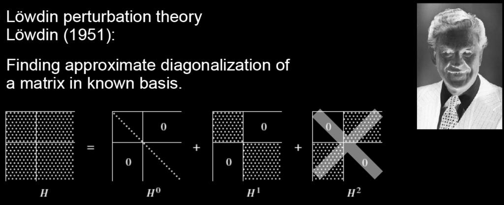
26 Loewdin Perturbation Theory A B 26
27 Loewdin Perturbation Theory Indices m, m', m'': Block A Indices l, l', l'' : Block B 27


28 Expansion Coefficients: BIA 28 [R. Winkler, Spin-Orbit Coupling Effects in Two-Dimensional Electron and Hole Systems, (2003)]


29 Expansion Coefficients: SIA 29 [R. Winkler, Spin-Orbit Coupling Effects in Two-Dimensional Electron and Hole Systems, (2003)]


30 Suitable Compounds 30
Spins and spin-orbit coupling in semiconductors, metals, and nanostructures
 B. Halperin Spin lecture 1 Spins and spin-orbit coupling in semiconductors, metals, and nanostructures Behavior of non-equilibrium spin populations. Spin relaxation and spin transport. How does one produce
Spin Transport in III-V Semiconductor Structures
 Spin Transport in III-V Semiconductor Structures Ki Wook Kim, A. A. Kiselev, and P. H. Song Department of Electrical and Computer Engineering, North Carolina State University, Raleigh, NC 27695-7911 We
Anisotropic spin splitting in InGaAs wire structures
 Available online at www.sciencedirect.com Physics Physics Procedia Procedia 3 (010) 00 (009) 155 159 000 000 14 th International Conference on Narrow Gap Semiconductors and Systems Anisotropic spin splitting
Electron spins in nonmagnetic semiconductors
 Electron spins in nonmagnetic semiconductors Yuichiro K. Kato Institute of Engineering Innovation, The University of Tokyo Physics of non-interacting spins Optical spin injection and detection Spin manipulation
Lok С. Lew Yan Voon Morten Willatzen. The k-p Method. Electronic Properties of Semiconductors. Springer
 Lok С. Lew Yan Voon Morten Willatzen The k-p Method Electronic Properties of Semiconductors Springer Acronyms xxi 1 Introduction 1 1.1 What Is к p Theory? 1 1.2 Electronic Properties of Semiconductors
Lecture I. Spin Orbitronics
 Lecture I Spin Orbitronics Alireza Qaiumzadeh Radboud University (RU) Institute for Molecules and Materials (IMM) Theory of Condensed Matter group (TCM) What We Talk About When We Talk About Spin Orbitronics
Project Report: Band Structure of GaAs using k.p-theory
 Proect Report: Band Structure of GaAs using k.p-theory Austin Irish Mikael Thorström December 12th 2017 1 Introduction The obective of the proect was to calculate the band structure of both strained and
ELECTRONS AND PHONONS IN SEMICONDUCTOR MULTILAYERS
 ELECTRONS AND PHONONS IN SEMICONDUCTOR MULTILAYERS Second Edition B.K. RIDLEY University of Essex CAMBRIDGE UNIVERSITY PRESS Contents Preface Introduction 1 Simple Models of the Electron-Phonon Interaction
QUANTUM WELLS, WIRES AND DOTS
 QUANTUM WELLS, WIRES AND DOTS Theoretical and Computational Physics of Semiconductor Nanostructures Second Edition Paul Harrison The University of Leeds, UK /Cf}\WILEY~ ^INTERSCIENCE JOHN WILEY & SONS,
Spin relaxation of conduction electrons Jaroslav Fabian (Institute for Theoretical Physics, Uni. Regensburg)
") Spin relaxation of conduction electrons Jaroslav Fabian (Institute for Theoretical Physics, Uni. Regensburg) :Syllabus: 1. Introductory description 2. Elliott-Yafet spin relaxation and spin hot spots 3.
Spin relaxation of conduction electrons Jaroslav Fabian (Institute for Theoretical Physics, Uni. Regensburg) :Syllabus: 1. Introductory description 2. Elliott-Yafet spin relaxation and spin hot spots 3.
Datta-Das type spin-field effect transistor in non-ballistic regime
 Datta-Das type spin-field effect transistor in non-ballistic regime Munekazu Ohno 1, Kanji Yoh 1,2 1 Research Center for Integrated Quantum Electronics, Hokkaido University, Sapporo, 060-8628, Japan 2
VERSION 4.0. Nanostructure semiconductor quantum simulation software for scientists and engineers.
 VERSION 4.0 Heterostructure Design Studio Nanostructure semiconductor quantum simulation software for scientists and engineers sales@optronicsdesign.com www.optronicsdesign.com Product description Heterostructure
Spintranszport és spindinamika nanorendszerekben Simon Ferenc
 Spintranszport és spindinamika nanorendszerekben Simon Ferenc BME Motivation Outline - Spintronics intro -Experimental methods -The Elliott-Yafet theory -Its generalization -Dessert Spintronics 1996 DARPA
Decay of spin polarized hot carrier current in a quasi. one-dimensional spin valve structure arxiv:cond-mat/ v1 [cond-mat.mes-hall] 10 Oct 2003
![Decay of spin polarized hot carrier current in a quasi. one-dimensional spin valve structure arxiv:cond-mat/ v1 [cond-mat.mes-hall] 10 Oct 2003](/thumbs/74/70335523.jpg "Decay of spin polarized hot carrier current in a quasi. one-dimensional spin valve structure arxiv:cond-mat/ v1 [cond-mat.mes-hall] 10 Oct 2003") Decay of spin polarized hot carrier current in a quasi one-dimensional spin valve structure arxiv:cond-mat/0310245v1 [cond-mat.mes-hall] 10 Oct 2003 S. Pramanik and S. Bandyopadhyay Department of Electrical
Decay of spin polarized hot carrier current in a quasi one-dimensional spin valve structure arxiv:cond-mat/0310245v1 [cond-mat.mes-hall] 10 Oct 2003 S. Pramanik and S. Bandyopadhyay Department of Electrical
Mn in GaAs: from a single impurity to ferromagnetic layers
 Mn in GaAs: from a single impurity to ferromagnetic layers Paul Koenraad Department of Applied Physics Eindhoven University of Technology Materials D e v i c e s S y s t e m s COBRA Inter-University Research
Electron Momentum and Spin Relaxation in Silicon Films
 Electron Momentum and Spin Relaxation in Silicon Films D. Osintsev, V. Sverdlov, and S. Selberherr Abstract Semiconductor spintronics is promising, because it allows creating microelectronic elements which
Experimental discovery of the spin-hall effect in Rashba spin-orbit coupled semiconductor systems
 Experimental discovery of the spin-hall effect in Rashba spin-orbit coupled semiconductor systems J. Wunderlich, 1 B. Kästner, 1,2 J. Sinova, 3 T. Jungwirth 4,5 1 Hitachi Cambridge Laboratory, Cambridge
Spin Lifetime Enhancement by Shear Strain in Thin Silicon-on-Insulator Films. Dmitry Osintsev, Viktor Sverdlov, and Siegfried Selberherr
 10.1149/05305.0203ecst The Electrochemical Society Spin Lifetime Enhancement by Shear Strain in Thin Silicon-on-Insulator Films Dmitry Osintsev, Viktor Sverdlov, and Siegfried Selberherr Institute for
Physics of Semiconductors
 Physics of Semiconductors 13 th 2016.7.11 Shingo Katsumoto Department of Physics and Institute for Solid State Physics University of Tokyo Outline today Laughlin s justification Spintronics Two current
Spin scattering by dislocations in III-V semiconductors
 PHYSICAL REVIEW B 70, 245203 (2004) Spin scattering by dislocations in III-V semiconductors Debdeep Jena* Department of Electrical Engineering, University of Notre Dame, Notre Dame, Indiana 46556, USA
Christian Scheller Physical Review Letters PRL 100, (2008)
") Christian Scheller 14.11.2008 Physical Review Letters PRL 100, 176806 (2008) Contents Overview D yakonov Perel spin relaxation Rashba effect Samples and symm. measurements (MPGE) Spin lifetime measurements
Christian Scheller 14.11.2008 Physical Review Letters PRL 100, 176806 (2008) Contents Overview D yakonov Perel spin relaxation Rashba effect Samples and symm. measurements (MPGE) Spin lifetime measurements
Persistent spin helix in spin-orbit coupled system. Joe Orenstein UC Berkeley and Lawrence Berkeley National Lab
 Persistent spin helix in spin-orbit coupled system Joe Orenstein UC Berkeley and Lawrence Berkeley National Lab Persistent spin helix in spin-orbit coupled system Jake Koralek, Chris Weber, Joe Orenstein
Lecture contents. Stress and strain Deformation potential. NNSE 618 Lecture #23
 1 Lecture contents Stress and strain Deformation potential Few concepts from linear elasticity theory : Stress and Strain 6 independent components 2 Stress = force/area ( 3x3 symmetric tensor! ) ij ji
Optically induced Hall effect in semiconductors
 Optically induced Hall effect in semiconductors M. Idrish Miah 1,2 and E. MacA. Gray 1 1 Nanoscale Science and Technology Centre, Griffith University, Nathan, Brisbane, QLD 4111, Australia. 2 Department
Inter-valence-band hole-hole scattering in cubic semiconductors
 PHYSICAL REVIEW B 73, 07537 006 Inter-valence-band hole-hole scattering in cubic semiconductors M. V. Dolguikh, A. V. Muravjov,* and R. E. Peale Department of Physics and College of Optics & Photonics,
Rashba spin-orbit coupling in the oxide 2D structures: The KTaO 3 (001) Surface
 Surface") Rashba spin-orbit coupling in the oxide 2D structures: The KTaO 3 (001) Surface Sashi Satpathy Department of Physics University of Missouri, Columbia, USA E Ref: K. V. Shanavas and S. Satpathy, Phys. Rev.
Rashba spin-orbit coupling in the oxide 2D structures: The KTaO 3 (001) Surface Sashi Satpathy Department of Physics University of Missouri, Columbia, USA E Ref: K. V. Shanavas and S. Satpathy, Phys. Rev.
Spin Dynamics in Single GaAs Nanowires
 1 Dr. Max Mustermann Referat Kommunikation & Marketing Verwaltung Spin Dynamics in Single GaAs Nanowires F. Dirnberger, S. Furthmeier, M. Forsch, A. Bayer, J. Hubmann, B. Bauer, J. Zweck, E. Reiger, C.
Removal of spin degeneracy in p-sige quantum wells demonstrated by spin photocurrents
 Removal of spin degeneracy in p-sige quantum wells demonstrated by spin photocurrents S. D. Ganichev, 1,2 U. Rössler, 1 W. Prettl, 1 E. L. Ivchenko, 2 V. V. Bel kov, 2 R. Neumann, 3 K. Brunner, 3 and G.
Lecture I. Spin Orbitronics
 Lecture I Spin Orbitronics Alireza Qaiumzadeh Radboud University (RU) Institute for Molecules and Materials (IMM) Theory of Condensed Matter group (TCM) What We Talk About When We Talk About Spin Orbitronics
Orbital Mechanisms of Electron- Spin Manipulation by an Electric Field
 Orbital Mechanisms of Electron- Spin Manipulation by an Electric Field The Harvard community has made this article openly available. Please share how this access benefits you. Your story matters Citation
SPINTRONICS. Waltraud Buchenberg. Faculty of Physics Albert-Ludwigs-University Freiburg
 SPINTRONICS Waltraud Buchenberg Faculty of Physics Albert-Ludwigs-University Freiburg July 14, 2010 TABLE OF CONTENTS 1 WHAT IS SPINTRONICS? 2 MAGNETO-RESISTANCE STONER MODEL ANISOTROPIC MAGNETO-RESISTANCE
Spin orbit interaction in semiconductors
 UNIVERSIDADE DE SÃO AULO Instituto de Física de São Carlos Spin orbit interaction in semiconductors J. Carlos Egues Instituto de Física de São Carlos Universidade de São aulo egues@ifsc.usp.br International
Dirac-Fermion-Induced Parity Mixing in Superconducting Topological Insulators. Nagoya University Masatoshi Sato
 Dirac-Fermion-Induced Parity Mixing in Superconducting Topological Insulators Nagoya University Masatoshi Sato In collaboration with Yukio Tanaka (Nagoya University) Keiji Yada (Nagoya University) Ai Yamakage
Calculation on the Band Structure of GaAs using k p -theory FFF042
 Calculation on the Band Structure of GaAs using k p -theory FFF04 I-Ju Chen, Sara Thorberg, Yang Chen December 17, 014 1 Introduction With its superior electronics and optical characteristics, GaAs is
Spin Dynamics in Semiconductors, Chapter 4 of Semiconductor Spintronics and Quantum Computation edited by D. D. Awschalom, D. Loss, and N. Samarth.
 Spin Dynamics in Semiconductors, Chapter 4 of Semiconductor Spintronics and Quantum Computation edited by D. D. Awschalom, D. Loss, and N. Samarth. Springer, New York, 2002. Contents 4 Spin Dynamics in
Notes on Topological Insulators and Quantum Spin Hall Effect. Jouko Nieminen Tampere University of Technology.
 Notes on Topological Insulators and Quantum Spin Hall Effect Jouko Nieminen Tampere University of Technology. Not so much discussed concept in this session: topology. In math, topology discards small details
Spin-Orbit Interactions in Semiconductor Nanostructures
 Spin-Orbit Interactions in Semiconductor Nanostructures Branislav K. Nikolić Department of Physics and Astronomy, University of Delaware, U.S.A. http://www.physics.udel.edu/~bnikolic Spin-Orbit Hamiltonians
Anomalous spin suscep.bility and suppressed exchange energy of 2D holes
 Anomalous spin suscep.bility and suppressed exchange energy of 2D holes School of Chemical and Physical Sciences & MacDiarmid Ins7tute for Advanced Materials and Nanotechnology Victoria University of Wellington
Spin transverse force on spin current in an electric field
 Title Spin transverse force on spin current in an electric field Author(s) Shen, SQ Citation Physical Review Letters, 005, v. 95 n. 18 Issued Date 005 URL http://hdl.handle.net/107/146197 Rights Physical
Supplementary Figures
 Supplementary Figures 8 6 Energy (ev 4 2 2 4 Γ M K Γ Supplementary Figure : Energy bands of antimonene along a high-symmetry path in the Brillouin zone, including spin-orbit coupling effects. Empty circles
Fundamental concepts of spintronics
 Fundamental concepts of spintronics Jaroslav Fabian Institute for Theoretical Physics University of Regensburg Stara Lesna, 24. 8. 2008 SFB 689 :outline: what is spintronics? spin injection spin-orbit
Nature, Vol 458, 2009 Leon Camenzind FMM University of Basel,
 Nature, Vol 458, 2009 Leon Camenzind University of Basel, 17.6.2011 Outlook Part I: Transient (Spin)-Grating Spectroscopy Part II: Theory of Persistent Spin Helix (PSH) Experimental results Part I Transient
Effective mass: from Newton s law. Effective mass. I.2. Bandgap of semiconductors: the «Physicist s approach» - k.p method
 Lecture 4 1/10/011 Effectie mass I.. Bandgap of semiconductors: the «Physicist s approach» - k.p method I.3. Effectie mass approximation - Electrons - Holes I.4. train effect on band structure - Introduction:
Strained Silicon, Electronic Band Structure and Related Issues.
 Strained Silicon, Electronic Band Structure and Related Issues. D. Rideau, F. Gilibert, M. Minondo, C. Tavernier and H. Jaouen STMicroelectronics,, Device Modeling 850 rue Jean Monnet, BP 16, F-38926 Crolles
PHYSICAL REVIEW B 71,
 Decoherence of transported spin in multichannel spin-orbit-coupled spintronic devices: Scattering approach to spin-density matrix from the ballistic to the localized regime Branislav K. Nikolić and Satofumi
Spin Currents in Mesoscopic Systems
 Spin Currents in Mesoscopic Systems Philippe Jacquod - U of Arizona I Adagideli (Sabanci) J Bardarson (Berkeley) M Duckheim (Berlin) D Loss (Basel) J Meair (Arizona) K Richter (Regensburg) M Scheid (Regensburg)
Problem 1: Spin 1 2. particles (10 points)
") Problem 1: Spin 1 particles 1 points 1 Consider a system made up of spin 1/ particles. If one measures the spin of the particles, one can only measure spin up or spin down. The general spin state of a
Problem 1: Spin 1 particles 1 points 1 Consider a system made up of spin 1/ particles. If one measures the spin of the particles, one can only measure spin up or spin down. The general spin state of a
VALENCE BAND STRUCTURE OF STRAINED-LAYER Si-Si0.5Ge0.5 SUPERLATTICES
 VALENCE BAND STRUCTURE OF STRAINED-LAYER Si-Si0.5Ge0.5 SUPERLATTICES U. Ekenberg, W. Batty, E. O Reilly To cite this version: U. Ekenberg, W. Batty, E. O Reilly. VALENCE BAND STRUCTURE OF STRAINED-LAYER
Lecture 9. Strained-Si Technology I: Device Physics
 Strain Analysis in Daily Life Lecture 9 Strained-Si Technology I: Device Physics Background Planar MOSFETs FinFETs Reading: Y. Sun, S. Thompson, T. Nishida, Strain Effects in Semiconductors, Springer,
Narrow-Gap Semiconductors, Spin Splitting With no Magnetic Field and more.. Giti Khodaparast Department of Physics Virginia Tech
 Narrow-Gap Semiconductors, Spin Splitting With no Magnetic Field and more.. Giti Khodaparast Department of Physics Virginia Tech Supported by: NFS-DMR-0507866 AFOSR Young Investigator Award University
M.S. Dresselhaus G. Dresselhaus A. Jorio. Group Theory. Application to the Physics of Condensed Matter. With 131 Figures and 219 Tables.
 M.S. Dresselhaus G. Dresselhaus A. Jorio Group Theory Application to the Physics of Condensed Matter With 131 Figures and 219 Tables 4) Springer Contents Part I Basic Mathematics 1 Basic Mathematical Background:
Improved Superlattices for Spin-Polarized Electron Sources
 SLAC-PUB-12249 December 2006 (ACCPHY/MATSCI) Improved Superlattices for Spin-Polarized Electron Sources Yu. A. Mamaev, L. G. Gerchikov, Yu. P. Yashin, V. Kuz michev, D. Vasiliev State Polytechnic University,
Spintronics: a step closer to the "The Emperor's New Mind" Ferenc Simon
 Spintronics: a step closer to the "The Emperor's New Mind" Ferenc Simon TU-Budapest, Institute of Physics Outline -I. Intro, spintronics -II. SOC,spin-relaxation mechanisms -III. The intuitive unified
Quantum Spin Hall Effect in Inverted Type II Semiconductors
 Quantum Spin Hall Effect in Inverted Type II Semiconductors Chaoxing Liu 1,2, Taylor L. Hughes 2, Xiao-Liang Qi 2, Kang Wang 3 and Shou-Cheng Zhang 2 1 Center for Advanced Study, Tsinghua University,Beijing,
Two-dimensional electron gases in heterostructures
 Two-dimensional electron gases in heterostructures 9 The physics of two-dimensional electron gases is very rich and interesting. Furthermore, two-dimensional electron gases in heterostructures are fundamental
Coherent Control of a Single Electron Spin with Electric Fields
 Coherent Control of a Single Electron Spin with Electric Fields Presented by Charulata Barge Graduate student Zumbühl Group Department of Physics, University of Basel Date:- 9-11-2007 Friday Group Meeting
Citation for published version (APA): Filip, A. T. (2002). Spin polarized electron transport in mesoscopic hybrid devices s.n.
: Filip, A. T. (2002). Spin polarized electron transport in mesoscopic hybrid devices s.n.") University of Groningen Spin polarized electron transport in mesoscopic hybrid devices Filip, Andrei Teodor IMPORTANT NOTE: You are advised to consult the publisher's version (publisher's PDF) if you wish
University of Groningen Spin polarized electron transport in mesoscopic hybrid devices Filip, Andrei Teodor IMPORTANT NOTE: You are advised to consult the publisher's version (publisher's PDF) if you wish
Energy Band Calculations for Dynamic Gain Models in Semiconductor Quantum Well Lasers
 Energy Band Calculations for Dynamic Gain Models in School of Electrical and Electronic Engineering University of Nottingham; Nottingham NG7 2RD; UK Email: eexpjb1@nottingham.ac.uk Presentation Outline
arxiv:cond-mat/ v1 25 Mar 2004
 Can an electric current orient spins in quantum wells? S.D. Ganichev 1,2, S.N. Danilov 1, Petra Schneider 1, V.V. Bel kov 2, L.E. Golub 2, W. Wegscheider 1, D. Weiss 1, W. Prettl 1 1 Fakultät Physik, University
Spin Filtering: how to write and read quantum information on mobile qubits
 Spin Filtering: how to write and read quantum information on mobile qubits Amnon Aharony Physics Department and Ilse Katz Nano institute Ora Entin-Wohlman (BGU), Guy Cohen (BGU) Yasuhiro Tokura (NTT) Shingo
arxiv:cond-mat/ v1 [cond-mat.mes-hall] 17 Sep 1997
![arxiv:cond-mat/ v1 [cond-mat.mes-hall] 17 Sep 1997](/thumbs/72/66504868.jpg "arxiv:cond-mat/ v1 [cond-mat.mes-hall] 17 Sep 1997") Multiband theory of quantum-dot quantum wells: Dark excitons, bright excitons, and charge separation in heteronanostructures arxiv:cond-mat/9709193v1 [cond-mat.mes-hall] 17 Sep 1997 W. Jaskólski and Garnett
Multiband theory of quantum-dot quantum wells: Dark excitons, bright excitons, and charge separation in heteronanostructures arxiv:cond-mat/9709193v1 [cond-mat.mes-hall] 17 Sep 1997 W. Jaskólski and Garnett
Spin-orbit coupling fields in Fe/GaAs heterostructures
 Spin-orbit coupling fields in Fe/GaAs heterostructures Outline motivation a simplified model of the Fe/GaAs heterostructure extracting spin-orbit coupling parameters spin-orbit coupling field conclusions
Acoustically induced spin relaxation in two-dimensional electronic systems
 Acoustically induced spin relaxation in two-dimensional electronic systems Dissertation zur Erlangung des akademischen Grades Dr. rer. nat. eingereicht an der Mathematisch-Naturwissenschaftlichen-Technischen
What so special about LaAlO3/SrTiO3 interface? Magnetism, Superconductivity and their coexistence at the interface
 What so special about LaAlO3/SrTiO3 interface? Magnetism, Superconductivity and their coexistence at the interface Pramod Verma Indian Institute of Science, Bangalore 560012 July 24, 2014 Pramod Verma
Anisotropic Current-Controlled Magnetization Reversal in the Ferromagnetic Semiconductor (Ga,Mn)As
As") Anisotropic Current-Controlled Magnetization Reversal in the Ferromagnetic Semiconductor (Ga,Mn)As Yuanyuan Li 1, Y. F. Cao 1, G. N. Wei 1, Yanyong Li 1, Y. i and K. Y. Wang 1,* 1 SKLSM, Institute of Semiconductors,
Anisotropic Current-Controlled Magnetization Reversal in the Ferromagnetic Semiconductor (Ga,Mn)As Yuanyuan Li 1, Y. F. Cao 1, G. N. Wei 1, Yanyong Li 1, Y. i and K. Y. Wang 1,* 1 SKLSM, Institute of Semiconductors,
Spin-polarization in quantum wires: Influence of Dresselhaus spin-orbit interaction and crosssection
 University of Richmond UR Scholarship Repository Physics Faculty Publications Physics 4-8-2009 Spin-polarization in quantum wires: Influence of Dresselhaus spin-orbit interaction and crosssection effects
Columnar quantum dots (QD) in polarization insensitive SOA and non-radiative Auger processes in QD: a theoretical study
 in polarization insensitive SOA and non-radiative Auger processes in QD: a theoretical study") olumnar quantum dots (QD) in polarization insensitive SOA and non-radiative Auger processes in QD: a theoretical study J. Even, L. Pedesseau, F. Doré, S. Boyer-Richard, UMR FOTON 68 NRS, INSA de Rennes,
olumnar quantum dots (QD) in polarization insensitive SOA and non-radiative Auger processes in QD: a theoretical study J. Even, L. Pedesseau, F. Doré, S. Boyer-Richard, UMR FOTON 68 NRS, INSA de Rennes,
Electric current-induced spin orientation in quantum well structures
 Journal of Magnetism and Magnetic Materials 3 (26) 127 131 www.elsevier.com/locate/jmmm Electric current-induced spin orientation in quantum well structures S.D. Ganichev a, S.N. Danilov a, Petra Schneider
arxiv: v2 [cond-mat.mes-hall] 14 Jul 2009
![arxiv: v2 [cond-mat.mes-hall] 14 Jul 2009](/thumbs/90/101396135.jpg "arxiv: v2 [cond-mat.mes-hall] 14 Jul 2009") Gate-controlled spin-orbit interaction in a parabolic GaAs/AlGaAs quantum well M. Studer, 1,2 G. Salis, 1 K. Ensslin, 2 D. C. Driscoll, 3 and A. C. Gossard 3 1 IBM Research, Zurich Research Laboratory,
Gate-controlled spin-orbit interaction in a parabolic GaAs/AlGaAs quantum well M. Studer, 1,2 G. Salis, 1 K. Ensslin, 2 D. C. Driscoll, 3 and A. C. Gossard 3 1 IBM Research, Zurich Research Laboratory,
Limitations in the Tunability of the Spin Resonance of 2D Electrons in Si by an Electric Current
 Vol. 112 (2007) ACTA PHYSICA POLONICA A No. 2 Proceedings of the XXXVI International School of Semiconducting Compounds, Jaszowiec 2007 Limitations in the Tunability of the Spin Resonance of 2D Electrons
Gauge Physics of Spin Hall Effect
 Gauge Physics of Spin Hall Effect (1) Data Storage Institute, A*STAR (Agency for Science, Technology and Research), DSI Building, 5 Engineering Drive 1, Singapore 117608 (2) Computational Nanoelectronics
Supporting Information for Quantized Conductance and Large g-factor Anisotropy in InSb Quantum Point Contacts
 Supporting Information for Quantized Conductance and Large g-factor Anisotropy in InSb Quantum Point Contacts Fanming Qu, Jasper van Veen, Folkert K. de Vries, Arjan J. A. Beukman, Michael Wimmer, Wei
Microelectronics Reliability
 Microelectronics Reliability xxx (2) xxx xxx Contents lists available at ScienceDirect Microelectronics Reliability journal homepage: www.elsevier.com/locate/microrel Modeling of enhancement factor of
Applicability of the k p method to the electronic structure of quantum dots
 PHYSICAL REVIEW B VOLUME, NUMBER 16 15 APRIL 1998-II Applicability of the k p method to the electronic structure of quantum dots Huaxiang Fu, Lin-Wang Wang, and Alex Zunger National Renewable Energy Laboratory,
InAs quantum dots: Predicted electronic structure of free-standing versus GaAs-embedded structures
 PHYSICAL REVIEW B VOLUME 59, NUMBER 24 15 JUNE 1999-II InAs quantum dots: Predicted electronic structure of free-standing versus GaAs-embedded structures A. J. Williamson and Alex Zunger National Renewable
SIGNATURES OF SPIN-ORBIT DRIVEN ELECTRONIC TRANSPORT IN TRANSITION- METAL-OXIDE INTERFACES
 SIGNATURES OF SPIN-ORBIT DRIVEN ELECTRONIC TRANSPORT IN TRANSITION- METAL-OXIDE INTERFACES Nicandro Bovenzi Bad Honnef, 19-22 September 2016 LAO/STO heterostructure: conducting interface between two insulators
Spin Hall and quantum spin Hall effects. Shuichi Murakami Department of Physics, Tokyo Institute of Technology PRESTO, JST
 YKIS2007 (Kyoto) Nov.16, 2007 Spin Hall and quantum spin Hall effects Shuichi Murakami Department of Physics, Tokyo Institute of Technology PRESTO, JST Introduction Spin Hall effect spin Hall effect in
Physics of Semiconductors (Problems for report)
") Physics of Semiconductors (Problems for report) Shingo Katsumoto Institute for Solid State Physics, University of Tokyo July, 0 Choose two from the following eight problems and solve them. I. Fundamentals
Physics of Semiconductors (Problems for report) Shingo Katsumoto Institute for Solid State Physics, University of Tokyo July, 0 Choose two from the following eight problems and solve them. I. Fundamentals
Defense Technical Information Center Compilation Part Notice
 UNCLASSIFIED Defense Technical Information Center Compilation Part Notice ADP013124 TITLE: Resonant Acceptors States in Ge/Ge[1-x]Si[x] MQW Hetero structures DISTRIBUTION: Approved for public release,
Energy Spectrum and Broken spin-surface locking in Topological Insulator quantum dots
 Energy Spectrum and Broken spin-surface locking in Topological Insulator quantum dots A. Kundu 1 1 Heinrich-Heine Universität Düsseldorf, Germany The Capri Spring School on Transport in Nanostructures
Charge transport in oxides and metalinsulator
 Charge transport in oxides and metalinsulator transitions M. Gabay School on modern topics in Condensed matter Singapore, 28/01 8/02 2013 Down the rabbit hole Scaling down impacts critical parameters of
Surface Majorana Fermions in Topological Superconductors. ISSP, Univ. of Tokyo. Nagoya University Masatoshi Sato
 Surface Majorana Fermions in Topological Superconductors ISSP, Univ. of Tokyo Nagoya University Masatoshi Sato Kyoto Tokyo Nagoya In collaboration with Satoshi Fujimoto (Kyoto University) Yoshiro Takahashi
Supplementary material: Nature Nanotechnology NNANO D
 Supplementary material: Nature Nanotechnology NNANO-06070281D Coercivities of the Co and Ni layers in the nanowire spin valves In the tri-layered structures used in this work, it is unfortunately not possible
PHYSICS OF SEMICONDUCTORS AND THEIR HETEROSTRUCTURES
 PHYSICS OF SEMICONDUCTORS AND THEIR HETEROSTRUCTURES Jasprit Singh University of Michigan McGraw-Hill, Inc. New York St. Louis San Francisco Auckland Bogota Caracas Lisbon London Madrid Mexico Milan Montreal
Surfaces, Interfaces, and Layered Devices
 Surfaces, Interfaces, and Layered Devices Building blocks for nanodevices! W. Pauli: God made solids, but surfaces were the work of Devil. Surfaces and Interfaces 1 Interface between a crystal and vacuum
From Last Time Important new Quantum Mechanical Concepts. Atoms and Molecules. Today. Symmetry. Simple molecules.
 Today From Last Time Important new Quantum Mechanical Concepts Indistinguishability: Symmetries of the wavefunction: Symmetric and Antisymmetric Pauli exclusion principle: only one fermion per state Spin
Supporting Information:
 Supporting Information: Strain Induced Optimization of Nanoelectromechanical Energy Harvesting and Nanopiezotronic Response in MoS 2 Monolayer Nanosheet Nityasagar Jena, Dimple, Shounak Dhananjay Behere,
Tunneling Spectroscopy of Disordered Two-Dimensional Electron Gas in the Quantum Hall Regime
 Tunneling Spectroscopy of Disordered Two-Dimensional Electron Gas in the Quantum Hall Regime The Harvard community has made this article openly available. Please share how this access benefits you. Your
Manipulation of Majorana fermions via single charge control
 Manipulation of Majorana fermions via single charge control Karsten Flensberg Niels Bohr Institute University of Copenhagen Superconducting hybrids: from conventional to exotic, Villard de Lans, France,
On depolarisation in 0D systems: Lamb-like level shift
 8th Int. Symp. Nanostructures: Physics and Technology St Petersburg, Russia, June 19 23, 2000 2000 Ioffe Institute QWR/QD.23p On depolarisation in 0D systems: Lamb-like level shift Slava V. Rotkin Ioffe
Accurate validation of experimental results of interdiffused. InGaAs/GaAs strained quantum wells by suitable numerical.
 Accurate validation of experimental results of interdiffused InGaAs/GaAs strained quantum wells by suitable numerical methods () Miguel Prol, Alfonso Moredo-Araújo, F. Javier Fraile-Peláez Dept. de Tecnologías
Performance Enhancement of P-channel InGaAs Quantum-well FETs by Superposition of Process-induced Uniaxial Strain and Epitaxially-grown Biaxial Strain
 Performance Enhancement of P-channel InGaAs Quantum-well FETs by Superposition of Process-induced Uniaxial Strain and Epitaxially-grown Biaxial Strain Ling Xia 1, Vadim Tokranov 2, Serge R. Oktyabrsky
Introduction to Optoelectronic Device Simulation by Joachim Piprek
 NUSOD 5 Tutorial MA Introduction to Optoelectronic Device Simulation by Joachim Piprek Outline:. Introduction: VCSEL Example. Electron Energy Bands 3. Drift-Diffusion Model 4. Thermal Model 5. Gain/Absorption
THEORY OF THE GAIN CHARACTERISTICS OF InGaN/AlGaN QD LASERS. A.D. Andreev * and E.P. O Reilly **
 THEORY OF THE GAIN CHARACTERISTICS OF InGaN/AlGaN QD LASERS A.D. Andreev * and E.P. O Reilly ** * A.F. Ioffe Physico-Technical Institute of Russian Academy of Sciences, Polytechnicheskaya 6, St.-Petersburg
Hartmut Buhmann. Physikalisches Institut, EP3 Universität Würzburg Germany
 Hartmut Buhmann Physikalisches Institut, EP3 Universität Würzburg Germany Part I and II Insulators and Topological Insulators HgTe crystal structure Part III quantum wells Two-Dimensional TI Quantum Spin
Tobias Dollinger Spin transport in two-dimensional electron and hole gases
 This dissertation focuses on spin based phenomena of transport in low-dimensional mesoscopic systems. The work contains the theoretical discussion of an experimentally verified spin-transistor concept,
Spin-orbit Effects in Semiconductor Spintronics. Laurens Molenkamp Physikalisches Institut (EP3) University of Würzburg
 University of Würzburg") Spin-orbit Effects in Semiconductor Spintronics Laurens Molenkamp Physikalisches Institut (EP3) University of Würzburg Collaborators Hartmut Buhmann, Charlie Becker, Volker Daumer, Yongshen Gui Matthias
Spin-orbit Effects in Semiconductor Spintronics Laurens Molenkamp Physikalisches Institut (EP3) University of Würzburg Collaborators Hartmut Buhmann, Charlie Becker, Volker Daumer, Yongshen Gui Matthias
Quantum Spin Hall Effect in Graphene
 Quantum Spin Hall Effect in Graphene Taylor S., Kai S., Benjamin S., Kathryn W., Penghao Z. C. L. Kane and E. J. Mele, Phys. Rev. Lett. 95, 226801 -- (2005) Quick Overview First the Motivation. Go over
Supporting Information
 Electronic Supplementary Material (ESI) for Nanoscale. This journal is The Royal Society of Chemistry 2015 Supporting Information Single Layer Lead Iodide: Computational Exploration of Structural, Electronic
STRAIN EFFECTS ON THE VALENCE BAND OF SILICON: PIEZORESISTANCE IN P-TYPE SILICON AND MOBILITY ENHANCEMENT IN STRAINED SILICON PMOSFET
 STRAIN EFFECTS ON THE VALENCE BAND OF SILICON: PIEZORESISTANCE IN P-TYPE SILICON AND MOBILITY ENHANCEMENT IN STRAINED SILICON PMOSFET By KEHUEY WU A DISSERTATION PRESENTED TO THE GRADUATE SCHOOL OF THE