Spin Transport in III-V Semiconductor Structures
|
|
|
- Norman Turner
- 6 years ago
- Views:
Transcription
1 Spin Transport in III-V Semiconductor Structures Ki Wook Kim, A. A. Kiselev, and P. H. Song Department of Electrical and Computer Engineering, North Carolina State University, Raleigh, NC We investigate theoretically spin-polarized transport and relaxation in III-V semiconductors including the 6.1-Å materials, and explore the possibility of its manipulation in practical nanoscale devices.
2 Mechanisms of spin relaxation* D'yakonov-Perel' (DP) mechanism: spin splitting of the conduction band at finite wave vectors is equivalent to effective magnetic field that causes electron spin to precess. It is random due to scattering in real space. Bir-Aronov-Pikus processes involve a simultaneous flip of electron and hole spins due to electron-hole exchange coupling. Spin relaxation due to momentum relaxation directly through spin-orbit coupling (Elliot-Yafet process). Spin relaxation due to carrier spin --- nuclear momentum interactions. *) G. E. Pikus and A. N. Titkov, in Optical Orientation, edited by F. Meier and B. P. Zakharchenya (Elsevier, 1994), p. 73.
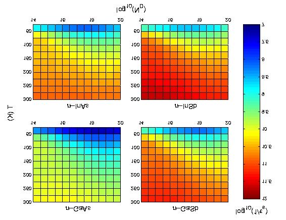
3 n-doped bulk semiconductors
4 p-doped bulk semiconductors
5 Relevant spin-relaxation mechanisms n-type Mostly, the DP mechanism dominates except of InSb, which is governed by the EY-mechanism in low T ( T < ~5 K) and at small doping concentrations (N D < ~10 18 cm -3 ). Analysis shows that the D'yakonov-Perel' mechanism is most relevant. p-type GaAs and GaSb: The DP and BAP mechanisms compete; the DP is dominant in high T and at small doping concentrations. InSb: The DP is dominating. InAs: There is a competition between the DP and the BAP for exc > 1 µev and the DP is dominating for exc < 1 µev
6 Spin splitting of conduction electrons for DP mechanism Bulk zinc-blende semiconductors - 2 x 2 conduction band Hamiltonian H = 2 h k 2m 2 e + η' ~ [ ( 2 2 σ k k k ) + cycl.perm. ] x x y z η ~ ' The constant reflects the strength of the spin splitting in the conduction band and it is defined by the details of the semiconductor band structure. The second (spin-dependent) term is equivalent to the presence of an effective magnetic field that causes electron spin to precess. 2D (001) heterostructures --- bulk Hamiltonian terms with k z2 will dominate due to strong spatial confinement. This reorients the effective magnetic field into the plane of the 2D electron gas (xy plane).
7 Bulk- vs. structure-asymmetry-induced spin splittings in 2D systems In addition to the bulk-induced terms in the effective Hamiltonian ( h 2) η' ( σ ν σ ν ), where η ' is derived from ~η ', / x x x y new (Bychkov-Rashba*) terms appear in asymmetric 2D heterostructures ( h 2) η ( σ ν σ ν ). / DP x y y x Constant η DP is defined by degree of the structure asymmetry and can be manipulated, i.e., by external electric field. Both types of terms individually have the same effect on the spin relaxation in heterostructures. We (arbitrarily) use Bychkov- Rashba term in our analysis. *) Yu. A. Bychkov and E. I. Rashba, Sov. Phys. JETP Lett. 39, 78 (1984).
8 D yakonov-perel mechanism in 2D 2 2 Hamiltonian in 2D structures with z = (0,0,1) defines spin precession in the effective magnetic field (that is random in the presence of electron scattering). H S = h ds σ Ωeff, =Ω eff S, Ω eff η DP ν z, 2 dt Random elementary rotations do not commute in 2D (and 3D). τ 1 S τ p Ω 2 eff
9 Possibilities to manipulate spin relaxation Regime of motional narrowing --- Since τ s -1 ~ τ p Ω eff2, reduction of momentum relaxation time, τ p, leads to the suppression of spin relaxation. Structure orientation --- Spin splitting is absent (small) for structures with principal axis along (011). External magnetic field --- Additional spin splitting, which is independent of electron wave vector will fix precession axis. Good candidate is the external magnetic field. Narrow channels of 2DEG --- DP spin relaxation in true 1D systems is absent, the question is --- How narrow the channel should be? Compensation of spin splittings --- Bulk- and structureasymmetry-induced spin terms in the Hamiltonian are additive. By manipulating structure asymmetry (i.e., by electric field), it is possible to tune combined splitting.
10 Monte Carlo model of quasi-1d electron spin transport Classical real-space movement. All particles have the same velocity v. Scattering is elastic and isotropic: no correlation between velocity directions before and after scattering events. Electron-electron interaction is neglected, all electrons are independent. Momentum relaxation time is τ p, distribution of times between scattering events is exponential (no correlation). Mean-free path is L p = v τ p Spin-rotating Hamiltonian is h h H S = σ Ωeff = ηdp σ xνy σ 2 2 Reflecting channel boundaries ( ν ) y x
11 Spin relaxation in a channel Apart from position-dependent spin rotation by angle φ = η DP r AB z, spin relaxation dependencies are essentially the same for all points. a) Decay of spin polarization is approximately exponential, so one can introduce spin relaxation time of electrons in the channel; b,c) Power-law scaling of τ s with L and η DP.
12 Regimes of spin relaxation in a channel η DP L p ~ elementary rotations during free flights are not small, τ s ~ τ p η DP L p << 1, η DP L ~ D spin relaxation, τ s 2D ~ τ p (η DP L p ) -2 η DP L << suppression of spin relaxation, quasi-1d regime, τ s ~ τ s 2D (η DP L) -2 L ~ L p --- L starts to act as L p, quantum mechanical quantization in the channel, intersubband scattering
13 Compensation of bulkand structure-induced splittings The bulk-asymmetry- (η ) and structure-asymmetry-induced (η DP ) spin terms are additive They are both linear-in-k and have similar but different form It is possible to tune η DP splitting to some desired value (say, η DP = ±η ), manipulating external electric field This allows to fix the axis of the effective magnetic field and suppress spin relaxation, as it happens in the pure 1D case.
14 New ballistic spin filter concept In spintronic* devices one needs to manipulate spin Conventional approach --- by external magnetic field micromagnets, ferromagnetic films, additional extensive circuitry, external magnets :-( Possible alternative --- intrinsic effect provided by spin-orbit (SO) interaction.** SO interaction by definition couples spin and orbit degrees of freedom *) G. A. Prinz, Physics Today 48(4), 58 (1995); Science 282, 1660 (1998). **) S. Datta and B. Das, Appl. Phys. Lett. 56, 665 (1990); Bulgakov, K. N. Pichugin, A. F. Sadreev, P. Streba, and P. Seba, Phys. Rev. Lett. 83, 376 (1999).
15 T-shaped 2D structure and others... x y Quasi-one dimensional channels formed from the two-dimensional electron gas (2DEG) using, e.g., electrostatic split-gate technique Special control electrode(s) are located over/under the structure (back and front gates) to manipulate SO interaction
16 Hamiltonian and other formulae 2D electron Hamiltonian (including spin part) Hˆ 2 k = h 2m 2 + V ( x, y) + { η( x, y) ( σˆ k σˆ k )} Channels are formed by hard walls (with boundary conditions uˆ S 0 ) or alternatively can be defined by the potential profile V ( x, y) (soft walls) x y y x The third dimension (i.e. z coordinate) is quantized. η reflects strength of the structure- or bulkasymmetry-induced spin-orbit (SO) interaction* *) Yu. A. Bychkov and E. I. Rashba, Sov. Phys. JETP Lett. 39, 78 (1984); G. Lommer, F. Malcher, and U. Rössler, Phys. Rev. B 32, 6965 (1985).
17 Manipulation of SO term by front/back gates E F Vfront Vback D. Grundler, Phys. Rev. Lett. 84, 6074 (2000). Independent variables: 1 V front + 2 η F ( V V ) 1 2 back ( V V ) front back
18 Model variables Incident electron energy Gate-induced potential 1 V Vfront + V 2 ( ) SO interaction coefficient 1 η Vfront V 2 back ( ) back x y Small front and back electrodes at the intersection: X 1+ e V () r, η(): r () 0 X r ( r r ) r = / 0
19 Real-life structure parameters Channel width w = 1000 Å Electron effective mass (InAs) m = 0.023m0 Quantization energy E = mev SO term parameter η0 = 180 mev Å (that is equal to 011 E w) Electrode radius r 0 = 2000 Å. 0
20 Polarization of the transmitted flux Transmission (per channel) Kinetic energy (in E 0 units) Spin polarization (%) Dashed line --- total polarization P Dotted --- difference between flux polarization in the + y and y 2 2 channels P + 1/ ( ) 2 x P z Solid --- total transmission
21 Modified structure: Asymmetric square ring Transmission (per channel) Kinetic energy (in E 0 units) Spin polarization (%) We have achieved simultaneously high transmission and high spin polarization of the transmitted flux.
22 Conclusion We have identified different regimes of the D yakonov-perel spin relaxation and analyzed dependencies of the spin relaxation time on the channel width L and DP parameter (inverse spin-rotation length) η DP. The most attractive for the future spintronic applications is a regime of the suppressed spin relaxation with the relaxation time, τ s, scaling as L DP -2 in narrow channels Functional ballistic spin devices can be designed that are based on the internal SO effect, modulated by control electrodes, that feature simultaneously high transmission efficiency and strong spin-dependent phenomena, including spin filtering and directional multiplexing
Decay of spin polarized hot carrier current in a quasi. one-dimensional spin valve structure arxiv:cond-mat/ v1 [cond-mat.mes-hall] 10 Oct 2003
![Decay of spin polarized hot carrier current in a quasi. one-dimensional spin valve structure arxiv:cond-mat/ v1 [cond-mat.mes-hall] 10 Oct 2003](/thumbs/74/70335523.jpg "Decay of spin polarized hot carrier current in a quasi. one-dimensional spin valve structure arxiv:cond-mat/ v1 [cond-mat.mes-hall] 10 Oct 2003") Decay of spin polarized hot carrier current in a quasi one-dimensional spin valve structure arxiv:cond-mat/0310245v1 [cond-mat.mes-hall] 10 Oct 2003 S. Pramanik and S. Bandyopadhyay Department of Electrical
Decay of spin polarized hot carrier current in a quasi one-dimensional spin valve structure arxiv:cond-mat/0310245v1 [cond-mat.mes-hall] 10 Oct 2003 S. Pramanik and S. Bandyopadhyay Department of Electrical
Datta-Das type spin-field effect transistor in non-ballistic regime
 Datta-Das type spin-field effect transistor in non-ballistic regime Munekazu Ohno 1, Kanji Yoh 1,2 1 Research Center for Integrated Quantum Electronics, Hokkaido University, Sapporo, 060-8628, Japan 2
Spin relaxation of conduction electrons Jaroslav Fabian (Institute for Theoretical Physics, Uni. Regensburg)
") Spin relaxation of conduction electrons Jaroslav Fabian (Institute for Theoretical Physics, Uni. Regensburg) :Syllabus: 1. Introductory description 2. Elliott-Yafet spin relaxation and spin hot spots 3.
Spin relaxation of conduction electrons Jaroslav Fabian (Institute for Theoretical Physics, Uni. Regensburg) :Syllabus: 1. Introductory description 2. Elliott-Yafet spin relaxation and spin hot spots 3.
Anisotropic spin splitting in InGaAs wire structures
 Available online at www.sciencedirect.com Physics Physics Procedia Procedia 3 (010) 00 (009) 155 159 000 000 14 th International Conference on Narrow Gap Semiconductors and Systems Anisotropic spin splitting
SPINTRONICS. Waltraud Buchenberg. Faculty of Physics Albert-Ludwigs-University Freiburg
 SPINTRONICS Waltraud Buchenberg Faculty of Physics Albert-Ludwigs-University Freiburg July 14, 2010 TABLE OF CONTENTS 1 WHAT IS SPINTRONICS? 2 MAGNETO-RESISTANCE STONER MODEL ANISOTROPIC MAGNETO-RESISTANCE
Spins and spin-orbit coupling in semiconductors, metals, and nanostructures
 B. Halperin Spin lecture 1 Spins and spin-orbit coupling in semiconductors, metals, and nanostructures Behavior of non-equilibrium spin populations. Spin relaxation and spin transport. How does one produce
Physics of Semiconductors
 Physics of Semiconductors 13 th 2016.7.11 Shingo Katsumoto Department of Physics and Institute for Solid State Physics University of Tokyo Outline today Laughlin s justification Spintronics Two current
Optically induced Hall effect in semiconductors
 Optically induced Hall effect in semiconductors M. Idrish Miah 1,2 and E. MacA. Gray 1 1 Nanoscale Science and Technology Centre, Griffith University, Nathan, Brisbane, QLD 4111, Australia. 2 Department
Conserved Spin Quantity in Strained Hole Systems with Rashba and Dresselhaus Spin-Orbit Coupling
 Conserved Spin Quantity in Strained Hole Systems with Rashba and Dresselhaus Spin-Orbit Coupling Paul Wenk, Michael Kammermeier, John Schliemann, Klaus Richter, Roland Winkler SFB Workshop Bernried 30.09.2014
Orbital Mechanisms of Electron- Spin Manipulation by an Electric Field
 Orbital Mechanisms of Electron- Spin Manipulation by an Electric Field The Harvard community has made this article openly available. Please share how this access benefits you. Your story matters Citation
Limitations in the Tunability of the Spin Resonance of 2D Electrons in Si by an Electric Current
 Vol. 112 (2007) ACTA PHYSICA POLONICA A No. 2 Proceedings of the XXXVI International School of Semiconducting Compounds, Jaszowiec 2007 Limitations in the Tunability of the Spin Resonance of 2D Electrons
The properties of the polaron in semiconductor quantum dots induced by influence of Rashba spin-orbit interaction
 J. At. Mol. Sci. doi: 1.48/jams.3111.431a Vol. 4, No., pp. 138-146 May 13 The properties of the polaron in semiconductor uantum dots induced by influence of Rashba spin-orbit interaction Xin-Jun Ma and
SEMICONDUCTOR SPINTRONICS FOR QUANTUM COMPUTATION
 SEMICONDUCTOR SPINTRONICS FOR QUANTUM COMPUTATION MICHAEL E. FLATTÉ (michael flatte@mailaps.org) Optical Science and Technology Center, Department of Physics and Astronomy, and Department of Electrical
ELECTRONS AND PHONONS IN SEMICONDUCTOR MULTILAYERS
 ELECTRONS AND PHONONS IN SEMICONDUCTOR MULTILAYERS Second Edition B.K. RIDLEY University of Essex CAMBRIDGE UNIVERSITY PRESS Contents Preface Introduction 1 Simple Models of the Electron-Phonon Interaction
Citation for published version (APA): Filip, A. T. (2002). Spin polarized electron transport in mesoscopic hybrid devices s.n.
: Filip, A. T. (2002). Spin polarized electron transport in mesoscopic hybrid devices s.n.") University of Groningen Spin polarized electron transport in mesoscopic hybrid devices Filip, Andrei Teodor IMPORTANT NOTE: You are advised to consult the publisher's version (publisher's PDF) if you wish
University of Groningen Spin polarized electron transport in mesoscopic hybrid devices Filip, Andrei Teodor IMPORTANT NOTE: You are advised to consult the publisher's version (publisher's PDF) if you wish
Transient grating measurements of spin diffusion. Joe Orenstein UC Berkeley and Lawrence Berkeley National Lab
 Transient grating measurements of spin diffusion Joe Orenstein UC Berkeley and Lawrence Berkeley National Lab LBNL, UC Berkeley and UCSB collaboration Chris Weber, Nuh Gedik, Joel Moore, JO UC Berkeley
Electron spins in nonmagnetic semiconductors
 Electron spins in nonmagnetic semiconductors Yuichiro K. Kato Institute of Engineering Innovation, The University of Tokyo Physics of non-interacting spins Optical spin injection and detection Spin manipulation
Effects of Quantum-Well Inversion Asymmetry on Electron- Nuclear Spin Coupling in the Fractional Quantum Hall Regime
 Effects of Quantum-Well Inversion Asymmetry on Electron- Nuclear Spin Coupling in the Fractional Quantum Hall Regime Katsushi Hashimoto,,2,a Koji Muraki,,b Norio Kumada, Tadashi Saku, 3 and Yoshiro Hirayama,2
Persistent spin helix in spin-orbit coupled system. Joe Orenstein UC Berkeley and Lawrence Berkeley National Lab
 Persistent spin helix in spin-orbit coupled system Joe Orenstein UC Berkeley and Lawrence Berkeley National Lab Persistent spin helix in spin-orbit coupled system Jake Koralek, Chris Weber, Joe Orenstein
Lecture I. Spin Orbitronics
 Lecture I Spin Orbitronics Alireza Qaiumzadeh Radboud University (RU) Institute for Molecules and Materials (IMM) Theory of Condensed Matter group (TCM) What We Talk About When We Talk About Spin Orbitronics
Mesoscopic Spintronics
 Mesoscopic Spintronics Taro WAKAMURA (Université Paris-Sud) Lecture 1 Today s Topics 1.1 History of Spintronics 1.2 Fudamentals in Spintronics Spin-dependent transport GMR and TMR effect Spin injection
Spin Dynamics in Semiconductors, Chapter 4 of Semiconductor Spintronics and Quantum Computation edited by D. D. Awschalom, D. Loss, and N. Samarth.
 Spin Dynamics in Semiconductors, Chapter 4 of Semiconductor Spintronics and Quantum Computation edited by D. D. Awschalom, D. Loss, and N. Samarth. Springer, New York, 2002. Contents 4 Spin Dynamics in
Spin-orbit Effects in Semiconductor Spintronics. Laurens Molenkamp Physikalisches Institut (EP3) University of Würzburg
 University of Würzburg") Spin-orbit Effects in Semiconductor Spintronics Laurens Molenkamp Physikalisches Institut (EP3) University of Würzburg Collaborators Hartmut Buhmann, Charlie Becker, Volker Daumer, Yongshen Gui Matthias
Spin-orbit Effects in Semiconductor Spintronics Laurens Molenkamp Physikalisches Institut (EP3) University of Würzburg Collaborators Hartmut Buhmann, Charlie Becker, Volker Daumer, Yongshen Gui Matthias
Influence of hyperfine interaction on optical orientation in self-assembled InAs/GaAs quantum dots
 Influence of hyperfine interaction on optical orientation in self-assembled InAs/GaAs quantum dots O. Krebs, B. Eble (PhD), S. Laurent (PhD), K. Kowalik (PhD) A. Kudelski, A. Lemaître, and P. Voisin Laboratoire
Supplementary material: Nature Nanotechnology NNANO D
 Supplementary material: Nature Nanotechnology NNANO-06070281D Coercivities of the Co and Ni layers in the nanowire spin valves In the tri-layered structures used in this work, it is unfortunately not possible
Spin injection and the local Hall effect in InAs quantum wells
 Spin injection and the local Hall effect in InAs quantum wells F.G. Monzon * and M.L. Roukes California Institute of Technology, Condensed Matter Physics 114-36, Pasadena CA 91125 We report on our efforts
Narrow-Gap Semiconductors, Spin Splitting With no Magnetic Field and more.. Giti Khodaparast Department of Physics Virginia Tech
 Narrow-Gap Semiconductors, Spin Splitting With no Magnetic Field and more.. Giti Khodaparast Department of Physics Virginia Tech Supported by: NFS-DMR-0507866 AFOSR Young Investigator Award University
Spin scattering by dislocations in III-V semiconductors
 PHYSICAL REVIEW B 70, 245203 (2004) Spin scattering by dislocations in III-V semiconductors Debdeep Jena* Department of Electrical Engineering, University of Notre Dame, Notre Dame, Indiana 46556, USA
QUANTUM INTERFERENCE IN SEMICONDUCTOR RINGS
 QUANTUM INTERFERENCE IN SEMICONDUCTOR RINGS PhD theses Orsolya Kálmán Supervisors: Dr. Mihály Benedict Dr. Péter Földi University of Szeged Faculty of Science and Informatics Doctoral School in Physics
Nuclear spin spectroscopy for semiconductor hetero and nano structures
 (Interaction and Nanostructural Effects in Low-Dimensional Systems) November 16th, Kyoto, Japan Nuclear spin spectroscopy for semiconductor hetero and nano structures Yoshiro Hirayama Tohoku University
Rashba spin-orbit coupling in the oxide 2D structures: The KTaO 3 (001) Surface
 Surface") Rashba spin-orbit coupling in the oxide 2D structures: The KTaO 3 (001) Surface Sashi Satpathy Department of Physics University of Missouri, Columbia, USA E Ref: K. V. Shanavas and S. Satpathy, Phys. Rev.
Rashba spin-orbit coupling in the oxide 2D structures: The KTaO 3 (001) Surface Sashi Satpathy Department of Physics University of Missouri, Columbia, USA E Ref: K. V. Shanavas and S. Satpathy, Phys. Rev.
Spring 2009 EE 710: Nanoscience and Engineering
 Spring 009 EE 710: Nanoscience and Engineering Part 8: Sprintronics Images and figures supplied from Goddard, et.al, Handbook of Nanoscience, Engineering, and Technology, CRC Press, 004 and other refereed
arxiv: v2 [cond-mat.mes-hall] 14 Jul 2009
![arxiv: v2 [cond-mat.mes-hall] 14 Jul 2009](/thumbs/90/101396135.jpg "arxiv: v2 [cond-mat.mes-hall] 14 Jul 2009") Gate-controlled spin-orbit interaction in a parabolic GaAs/AlGaAs quantum well M. Studer, 1,2 G. Salis, 1 K. Ensslin, 2 D. C. Driscoll, 3 and A. C. Gossard 3 1 IBM Research, Zurich Research Laboratory,
Gate-controlled spin-orbit interaction in a parabolic GaAs/AlGaAs quantum well M. Studer, 1,2 G. Salis, 1 K. Ensslin, 2 D. C. Driscoll, 3 and A. C. Gossard 3 1 IBM Research, Zurich Research Laboratory,
Electron Momentum and Spin Relaxation in Silicon Films
 Electron Momentum and Spin Relaxation in Silicon Films D. Osintsev, V. Sverdlov, and S. Selberherr Abstract Semiconductor spintronics is promising, because it allows creating microelectronic elements which
Max-Planck-Institut für Metallforschung Stuttgart. Towards Spin Injection into Silicon. Saroj Prasad Dash. Dissertation an der Universität Stuttgart
 Max-Planck-Institut für Metallforschung Stuttgart Towards Spin Injection into Silicon Saroj Prasad Dash Dissertation an der Universität Stuttgart Bericht Nr. 203 August 2007 Towards Spin Injection into
Spin-resolved Hall effect driven by spin-orbit coupling. Physical Review B - Condensed Matter And Materials Physics, 2005, v. 71 n.
 Title Spin-resolved Hall effect driven by spin-orbit coupling Author(s) Li, J; Hu, L; Shen, SQ Citation Physical Review B - Condensed Matter And Materials Physics, 2005, v. 71 n. 24 Issued Date 2005 URL
Lecture 8, April 12, 2017
 Lecture 8, April 12, 2017 This week (part 2): Semiconductor quantum dots for QIP Introduction to QDs Single spins for qubits Initialization Read-Out Single qubit gates Book on basics: Thomas Ihn, Semiconductor
Spin scattering in nonmagnetic semiconductors
 Spin scattering in nonmagnetic semiconductors Spin state Wave function: ψ Spin densit matri: ρ ψ OR, s ϕ, ϕ, ρ ρ, s ψ, s ρ ρ In general, it should be ρ, ; s, s Use Wigner s function to get ρ K, R; s, s
Effect of Spin-Orbit Interaction and In-Plane Magnetic Field on the Conductance of a Quasi-One-Dimensional System
 ArXiv : cond-mat/0311143 6 November 003 Effect of Spin-Orbit Interaction and In-Plane Magnetic Field on the Conductance of a Quasi-One-Dimensional System Yuriy V. Pershin, James A. Nesteroff, and Vladimir
Spin Filtering: how to write and read quantum information on mobile qubits
 Spin Filtering: how to write and read quantum information on mobile qubits Amnon Aharony Physics Department and Ilse Katz Nano institute Ora Entin-Wohlman (BGU), Guy Cohen (BGU) Yasuhiro Tokura (NTT) Shingo
Chapter 3 Properties of Nanostructures
 Chapter 3 Properties of Nanostructures In Chapter 2, the reduction of the extent of a solid in one or more dimensions was shown to lead to a dramatic alteration of the overall behavior of the solids. Generally,
Spin Lifetime Enhancement by Shear Strain in Thin Silicon-on-Insulator Films. Dmitry Osintsev, Viktor Sverdlov, and Siegfried Selberherr
 10.1149/05305.0203ecst The Electrochemical Society Spin Lifetime Enhancement by Shear Strain in Thin Silicon-on-Insulator Films Dmitry Osintsev, Viktor Sverdlov, and Siegfried Selberherr Institute for
arxiv: v2 [cond-mat.mes-hall] 6 Dec 2018
![arxiv: v2 [cond-mat.mes-hall] 6 Dec 2018](/thumbs/91/107326502.jpg "arxiv: v2 [cond-mat.mes-hall] 6 Dec 2018") Spin splitting and switching effect in a four-terminal two-dimensional electron gas nanostructure Zijiang Wang 1, Jianhong He 1,2, Huazhong Guo 1 1 Laboratory of Mesoscopic and Low Dimensional Physics,
Spin splitting and switching effect in a four-terminal two-dimensional electron gas nanostructure Zijiang Wang 1, Jianhong He 1,2, Huazhong Guo 1 1 Laboratory of Mesoscopic and Low Dimensional Physics,
PHYSICAL REVIEW B 71,
 Decoherence of transported spin in multichannel spin-orbit-coupled spintronic devices: Scattering approach to spin-density matrix from the ballistic to the localized regime Branislav K. Nikolić and Satofumi
Christian Scheller Physical Review Letters PRL 100, (2008)
") Christian Scheller 14.11.2008 Physical Review Letters PRL 100, 176806 (2008) Contents Overview D yakonov Perel spin relaxation Rashba effect Samples and symm. measurements (MPGE) Spin lifetime measurements
Christian Scheller 14.11.2008 Physical Review Letters PRL 100, 176806 (2008) Contents Overview D yakonov Perel spin relaxation Rashba effect Samples and symm. measurements (MPGE) Spin lifetime measurements
Spin relaxation of two-dimensional electrons with a hierarchy of spin orbit couplings
 IOP PUBLISHING JOURNAL OF PHYSICS: CONDENSED MATTER J. Phys.: Condens. Matter 9 (007) 3463 (pp) doi:0.088/0953-8984/9/34/3463 Spin relaxation of two-dimensional electrons with a hierarchy of spin orbit
Ballistic Electron Spectroscopy of Quantum Mechanical Anti-reflection Coatings for GaAs/AlGaAs Superlattices
 Ballistic Electron Spectroscopy of Quantum Mechanical Anti-reflection Coatings for GaAs/AlGaAs Superlattices C. Pacher, M. Kast, C. Coquelin, G. Fasching, G. Strasser, E. Gornik Institut für Festkörperelektronik,
SUPPLEMENTARY INFORMATION
 SUPPLEMENTARY INFORMATION DOI: 10.1038/NNANO.2014.16 Electrical detection of charge current-induced spin polarization due to spin-momentum locking in Bi 2 Se 3 by C.H. Li, O.M.J. van t Erve, J.T. Robinson,
Spin relaxation in low-dimensional systems
 J. Phys.: Condens. Matter 11 (1999) 5929 5952. Printed in the UK PII: S0953-8984(99)01386-7 Spin relaxation in low-dimensional systems LViña Departamento de Física de Materiales C-IV-510, Universidad Autónoma
Fundamental concepts of spintronics
 Fundamental concepts of spintronics Jaroslav Fabian Institute for Theoretical Physics University of Regensburg Stara Lesna, 24. 8. 2008 SFB 689 :outline: what is spintronics? spin injection spin-orbit
Mesoscopic Spin Hall Effect in Multiprobe Semiconductor Bridges
 Mesoscopic Spin Hall Effect in Multiprobe Semiconductor Bridges Branislav K. Nikolić, Liviu P. Zârbo, and Satofumi Souma Department of Physics and Astronomy, University of Delaware, Newark, DE 19716-2570
Surfaces, Interfaces, and Layered Devices
 Surfaces, Interfaces, and Layered Devices Building blocks for nanodevices! W. Pauli: God made solids, but surfaces were the work of Devil. Surfaces and Interfaces 1 Interface between a crystal and vacuum
SUPPLEMENTARY INFORMATION
 Supporting online material SUPPLEMENTARY INFORMATION doi: 0.038/nPHYS8 A: Derivation of the measured initial degree of circular polarization. Under steady state conditions, prior to the emission of the
UTILIZATION of spin-dependent phenomena in electronic
 IEEE TRANSACTIONS ON NANOTECHNOLOGY, VOL. 3, NO. 1, MARCH 2004 173 Study of Spin-Polarized Transport Properties for Spin-FET Design Optimization Semion Saikin, Min Shen, and Ming-C. Cheng, Member, IEEE
Spin and phase coherence times in Te doped InSb thin films
 Physics Procedia Physics Physics Procedia Procedia 3 (2010) 00 (2009) 1237 1242 1 6 www.elsevier.com/locate/procedia 14 th International Conference on Narrow Gap Semiconductors and Systems Spin and phase
ISSN: [bhardwaj* et al., 5(11): November, 2016] Impact Factor: 4.116
![ISSN: [bhardwaj* et al., 5(11): November, 2016] Impact Factor: 4.116](/thumbs/87/97249459.jpg "ISSN: [bhardwaj* et al., 5(11): November, 2016] Impact Factor: 4.116") ISSN: 77-9655 [bhardwaj* et al., 5(11): November, 016] Impact Factor: 4.116 IJESRT INTERNATIONAL JOURNAL OF ENGINEERING SCIENCES & RESEARCH TECHNOLOGY EXCITON BINDING ENERGY IN BULK AND QUANTUM WELL OF
ISSN: 77-9655 [bhardwaj* et al., 5(11): November, 016] Impact Factor: 4.116 IJESRT INTERNATIONAL JOURNAL OF ENGINEERING SCIENCES & RESEARCH TECHNOLOGY EXCITON BINDING ENERGY IN BULK AND QUANTUM WELL OF
Theory of spin-polarized transport in photoexcited semiconductor/ferromagnet tunnel junctions
 PHYSICAL REVIEW B VOLUME 57, NUMBER 7 15 FEBRUARY 1998-I Theory of spin-polarized transport in photoexcited semiconductor/ferromagnet tunnel junctions R. Jansen,* M. W. J. Prins, and H. van Kempen Research
Theory of electrical spin injection: Tunnel contacts as a solution of the conductivity mismatch problem
 Theory of electrical spin injection: Tunnel contacts as a solution of the conductivity mismatch problem The Harvard community has made this article openly available. Please share how this access benefits
Spin and charge transport in the presence of spin-orbit interaction
 PRAMANA cfl Indian Academy of Sciences Vol. 58, No. 2 journal of February 2002 physics pp. 293 311 Spin and charge transport in the presence of spin-orbit interaction T P PAREEK and P BRUNO Max-Planck-Institute
Spin Dynamics in Single GaAs Nanowires
 1 Dr. Max Mustermann Referat Kommunikation & Marketing Verwaltung Spin Dynamics in Single GaAs Nanowires F. Dirnberger, S. Furthmeier, M. Forsch, A. Bayer, J. Hubmann, B. Bauer, J. Zweck, E. Reiger, C.
Nature, Vol 458, 2009 Leon Camenzind FMM University of Basel,
 Nature, Vol 458, 2009 Leon Camenzind University of Basel, 17.6.2011 Outlook Part I: Transient (Spin)-Grating Spectroscopy Part II: Theory of Persistent Spin Helix (PSH) Experimental results Part I Transient
Spin-Polarized Current in Coulomb Blockade and Kondo Regime
 Vol. 112 (2007) ACTA PHYSICA POLONICA A No. 2 Proceedings of the XXXVI International School of Semiconducting Compounds, Jaszowiec 2007 Spin-Polarized Current in Coulomb Blockade and Kondo Regime P. Ogrodnik
(a) (b) Supplementary Figure 1. (a) (b) (a) Supplementary Figure 2. (a) (b) (c) (d) (e)
 (b) Supplementary Figure 1. (a) (b) (a) Supplementary Figure 2. (a) (b) (c) (d) (e)") (a) (b) Supplementary Figure 1. (a) An AFM image of the device after the formation of the contact electrodes and the top gate dielectric Al 2 O 3. (b) A line scan performed along the white dashed line
(a) (b) Supplementary Figure 1. (a) An AFM image of the device after the formation of the contact electrodes and the top gate dielectric Al 2 O 3. (b) A line scan performed along the white dashed line
Photogalvanic eects in quantum wells
 Physica E 14 () 166 171 www.elsevier.com/locate/physe Photogalvanic eects in quantum wells S.D. Ganichev a;b;, E.L. Ivchenko b, W. Prettl a a Institut fur Exp. und Angew. Physik, Universitat Regensburg,
arxiv:cond-mat/ v2 [cond-mat.mtrl-sci] 6 Dec 2002
![arxiv:cond-mat/ v2 [cond-mat.mtrl-sci] 6 Dec 2002](/thumbs/72/67701169.jpg "arxiv:cond-mat/ v2 [cond-mat.mtrl-sci] 6 Dec 2002") Magnetic-field dependence of electron spin relaxation in n-type semiconductors Franz X. Bronold, 1,2 Ivar Martin, 2 Avadh Saxena, 2 and Darryl L. Smith 2 1 Institut für Physik, Ernst-Moritz-Arndt Universität
Magnetic-field dependence of electron spin relaxation in n-type semiconductors Franz X. Bronold, 1,2 Ivar Martin, 2 Avadh Saxena, 2 and Darryl L. Smith 2 1 Institut für Physik, Ernst-Moritz-Arndt Universität
Zeeman splitting of single semiconductor impurities in resonant tunneling heterostructures
 Superlattices and Microstructures, Vol. 2, No. 4, 1996 Zeeman splitting of single semiconductor impurities in resonant tunneling heterostructures M. R. Deshpande, J. W. Sleight, M. A. Reed, R. G. Wheeler
Defense Technical Information Center Compilation Part Notice
 UNCLASSIFIED Defense Technical Information Center Compilation Part Notice ADP013209 TITLE: Polarized Electron Photoemission Studies of Spin Relaxation in Thin GaAs Epitaxial Films DISTRIBUTION: Approved
Spin-orbit effects in single-electron states in coupled quantum dots
 PHYSICAL REVIEW B 7, 155410 005 Spin-orbit effects in single-electron states in coupled quantum dots Peter Stano 1, and Jaroslav Fabian 1, 1 Institute of Physics, Karl-Franzens University, Universitätsplatz
Spin-Orbit Interactions in Semiconductor Nanostructures
 Spin-Orbit Interactions in Semiconductor Nanostructures Branislav K. Nikolić Department of Physics and Astronomy, University of Delaware, U.S.A. http://www.physics.udel.edu/~bnikolic Spin-Orbit Hamiltonians
PROOF COPY [BT9347] PRB
![PROOF COPY [BT9347] PRB](/thumbs/84/91030426.jpg "PROOF COPY [BT9347] PRB") PHYSICAL REVIEW B 70, 1() Spin-dependent transport of electrons in the presence of a smooth lateral potential and spin-orbit interaction Alexander O. Govorov, 1 Alexander V. Kalameitsev, 2 and John P.
PHYSICAL REVIEW B 70, 1() Spin-dependent transport of electrons in the presence of a smooth lateral potential and spin-orbit interaction Alexander O. Govorov, 1 Alexander V. Kalameitsev, 2 and John P.
arxiv:cond-mat/ v1 25 Mar 2004
 Can an electric current orient spins in quantum wells? S.D. Ganichev 1,2, S.N. Danilov 1, Petra Schneider 1, V.V. Bel kov 2, L.E. Golub 2, W. Wegscheider 1, D. Weiss 1, W. Prettl 1 1 Fakultät Physik, University
Optically pumped transport in ferromagnet-semiconductor Schottky diodes invited
 JOURNAL OF APPLIED PHYSICS VOLUME 91, NUMBER 10 15 MAY 2002 Optically pumped transport in ferromagnet-semiconductor Schottky diodes invited A. F. Isakovic School of Physics and Astronomy, University of
Spin Orbit Coupling (SOC) in Graphene
 in Graphene") Spin Orbit Coupling (SOC) in Graphene MMM, Mirko Rehmann, 12.10.2015 Motivation Weak intrinsic SOC in graphene: [84]: Phys. Rev. B 80, 235431 (2009) [85]: Phys. Rev. B 82, 125424 (2010) [86]: Phys. Rev.
Spin Orbit Coupling (SOC) in Graphene MMM, Mirko Rehmann, 12.10.2015 Motivation Weak intrinsic SOC in graphene: [84]: Phys. Rev. B 80, 235431 (2009) [85]: Phys. Rev. B 82, 125424 (2010) [86]: Phys. Rev.
Tunable spin Hall effect by Stern-Gerlach diffraction
 Tunable spin Hall effect by Stern-Gerlach diffraction Jun-Qiang Lu and X.-G. Zhang Center for Nanophase Materials Sciences, and Computer Science and Mathematics Division, Oak Ridge National Laboratory,
All-electrical measurements of direct spin Hall effect in GaAs with Esaki diode electrodes.
 All-electrical measurements of direct spin Hall effect in GaAs with Esaki diode electrodes. M. Ehlert 1, C. Song 1,2, M. Ciorga 1,*, M. Utz 1, D. Schuh 1, D. Bougeard 1, and D. Weiss 1 1 Institute of Experimental
Lecture 20: Semiconductor Structures Kittel Ch 17, p , extra material in the class notes
 Lecture 20: Semiconductor Structures Kittel Ch 17, p 494-503, 507-511 + extra material in the class notes MOS Structure Layer Structure metal Oxide insulator Semiconductor Semiconductor Large-gap Semiconductor
arxiv: v2 [cond-mat.mes-hall] 6 Apr 2011
![arxiv: v2 [cond-mat.mes-hall] 6 Apr 2011](/thumbs/72/66469363.jpg "arxiv: v2 [cond-mat.mes-hall] 6 Apr 2011") Electron spin relaxation as evidence of excitons in a two dimensional electron-hole plasma arxiv:1103.2474v2 [cond-mat.mes-hall] 6 Apr 2011 S. Oertel, 1 S. Kunz, 1 D. Schuh, 2 W. Wegscheider, 3 J. Hübner,
Electron spin relaxation as evidence of excitons in a two dimensional electron-hole plasma arxiv:1103.2474v2 [cond-mat.mes-hall] 6 Apr 2011 S. Oertel, 1 S. Kunz, 1 D. Schuh, 2 W. Wegscheider, 3 J. Hübner,
Spin and Charge transport in Ferromagnetic Graphene
 Spin and Charge transport in Ferromagnetic Graphene Hosein Cheraghchi School of Physics, Damghan University Recent Progress in D Systems, Oct, 4, IPM Outline: Graphene Spintronics Background on graphene
Mechanical effects of light spin and orbital angular momentum in liquid crystals
 Mechanical effects of light spin and orbital angular momentum in liquid crystals E.Santamato Università degli Studi di Napoli Federico II Dipartimento di Scienze Fisiche Complesso di Monte S. Angelo via
Semiconductor Spintronics
 Semiconductor Spintronics Junsaku Nitta Abstract In semiconductor spintronics, electron spin rather than charge is the key property. This paper describes several spin-related devices using spin-orbit interaction.
Spintranszport és spindinamika nanorendszerekben Simon Ferenc
 Spintranszport és spindinamika nanorendszerekben Simon Ferenc BME Motivation Outline - Spintronics intro -Experimental methods -The Elliott-Yafet theory -Its generalization -Dessert Spintronics 1996 DARPA
Intersubband Response:
 Intersubband Response: Lineshape,, Coulomb Renormalization, and Microcavity Effects F. T. Vasko Inst. of Semiconductor Physics Kiev, Ukraine In collaboration with: A.V. Korovin and O.E. Raichev (Inst.
Spintronics at Nanoscale
 Colloquium@NTHU Sep 22, 2004 Spintronics at Nanoscale Hsiu-Hau Lin Nat l Tsing-Hua Univ & Nat l Center for Theoretical Sciences What I have been doing Spintronics: Green s function theory for diluted magnetic
Two-dimensional electron gases in heterostructures
 Two-dimensional electron gases in heterostructures 9 The physics of two-dimensional electron gases is very rich and interesting. Furthermore, two-dimensional electron gases in heterostructures are fundamental
What is Quantum Transport?
 What is Quantum Transport? Branislav K. Nikolić Department of Physics and Astronomy, University of Delaware, U.S.A. http://www.physics.udel.edu/~bnikolic Semiclassical Transport (is boring!) Bloch-Boltzmann
Lecture contents. Stress and strain Deformation potential. NNSE 618 Lecture #23
 1 Lecture contents Stress and strain Deformation potential Few concepts from linear elasticity theory : Stress and Strain 6 independent components 2 Stress = force/area ( 3x3 symmetric tensor! ) ij ji
Interference of magnetointersubband and phonon-induced resistance oscillations in single GaAs quantum wells with two populated subbands
 Interference of magnetointersubband and phonon-induced resistance oscillations in single GaAs quantum wells with two populated subbands A.A.Bykov and A.V.Goran Institute of Semiconductor Physics, Russian
Electrical control of spin relaxation in a quantum dot. S. Amasha et al., condmat/
 Electrical control of spin relaxation in a quantum dot S. Amasha et al., condmat/07071656 Spin relaxation In a magnetic field, spin states are split b the Zeeman energ = g µ B B Provides a two-level sstem
Spintronics: a step closer to the "The Emperor's New Mind" Ferenc Simon
 Spintronics: a step closer to the "The Emperor's New Mind" Ferenc Simon TU-Budapest, Institute of Physics Outline -I. Intro, spintronics -II. SOC,spin-relaxation mechanisms -III. The intuitive unified
NONLINEAR TRANSITIONS IN SINGLE, DOUBLE, AND TRIPLE δ-doped GaAs STRUCTURES
 NONLINEAR TRANSITIONS IN SINGLE, DOUBLE, AND TRIPLE δ-doped GaAs STRUCTURES E. OZTURK Cumhuriyet University, Faculty of Science, Physics Department, 58140 Sivas-Turkey E-mail: eozturk@cumhuriyet.edu.tr
Polarization-induced Rashba spin-orbit coupling in structurally symmetric III-Nitride quantum wells
 Polarization-induced Rashba spin-orbit coupling in structurally symmetric III-Nitride quantum wells V.I. Litvinov * WaveBand/ Sierra Nevada Corporation, 545 Alton Parkway, Suite 00, Irvine, CA 968 PACS
Saroj P. Dash. Chalmers University of Technology. Göteborg, Sweden. Microtechnology and Nanoscience-MC2
 Silicon Spintronics Saroj P. Dash Chalmers University of Technology Microtechnology and Nanoscience-MC2 Göteborg, Sweden Acknowledgement Nth Netherlands University of Technology Sweden Mr. A. Dankert Dr.
Electric current-induced spin orientation in quantum well structures
 Journal of Magnetism and Magnetic Materials 3 (26) 127 131 www.elsevier.com/locate/jmmm Electric current-induced spin orientation in quantum well structures S.D. Ganichev a, S.N. Danilov a, Petra Schneider
File name: Supplementary Information Description: Supplementary Figures and Supplementary References. File name: Peer Review File Description:
 File name: Supplementary Information Description: Supplementary Figures and Supplementary References File name: Peer Review File Description: Supplementary Figure Electron micrographs and ballistic transport
IOP Conference Series: Materials Science and Engineering. Related content PAPER OPEN ACCESS
 IOP Conference Series: Materials Science and Engineering PAPER OPEN ACCESS Comparison of Electron Transmittance and Tunneling Current through a Trapezoidal Potential Barrier with Spin Polarization Consideration
Magnetosubbands of semiconductor quantum wires with Rashba spin-orbit coupling
 PHYSICAL REVIEW B 71, 035311 2005 Magnetosubbands of semiconductor quantum wires with Rashba spin-orbit coupling J. Knobbe and Th. Schäpers* Institut für Schichten und Grenzflächen and Center of Nanoelectronic
Topological Insulators and Ferromagnets: appearance of flat surface bands
 Topological Insulators and Ferromagnets: appearance of flat surface bands Thomas Dahm University of Bielefeld T. Paananen and T. Dahm, PRB 87, 195447 (2013) T. Paananen et al, New J. Phys. 16, 033019 (2014)
Anomalous spin suscep.bility and suppressed exchange energy of 2D holes
 Anomalous spin suscep.bility and suppressed exchange energy of 2D holes School of Chemical and Physical Sciences & MacDiarmid Ins7tute for Advanced Materials and Nanotechnology Victoria University of Wellington
Transport properties through double-magnetic-barrier structures in graphene
 Chin. Phys. B Vol. 20, No. 7 (20) 077305 Transport properties through double-magnetic-barrier structures in graphene Wang Su-Xin( ) a)b), Li Zhi-Wen( ) a)b), Liu Jian-Jun( ) c), and Li Yu-Xian( ) c) a)
Cleveland, OH 44106, USA *
 Control of valley polarization in monolayer MoS 2 by optical helicity Kin Fai Mak 1, Keliang He 2, Jie Shan 2, and Tony F. Heinz 1* 1 Departments of Physics and Electrical Engineering, Columbia University,