Direct Measurements of Irradiation-Induced Creep in Micropillars of Amorphous Cu 56 Ti 38 Ag 6, Zr 52 Ni 48, Si and SiO 2
|
|
|
- Godwin Greene
- 5 years ago
- Views:
Transcription
1 Direct Measurements of Irradiation-Induced Creep in Micropillars of Amorphous Cu 56 Ti 38 Ag 6, Zr 52 Ni 48, Si and SiO 2 Sezer Özerinç, 1 Hoe Joon Kim, 1 Robert S. Averback, 2 and William P. King 1,2,a) 1 Department of Mechanical Science and Engineering, University of Illinois at Urbana-Champaign, Urbana, Illinois, 61801, USA 2 Department of Materials Science and Engineering, University of Illinois at Urbana-Champaign, Urbana, Illinois, 61801, USA We report in situ measurements of irradiation-induced creep on amorphous (a-) Cu 56 Ti 38 Ag 6, Zr 52 Ni 48, Si, and SiO 2. Micropillars 1 µm in diameter and 2 µm in height were irradiated with ~2 MeV heavy ions during uniaxial compression at room temperature. The creep measurements were performed using a custom mechanical testing apparatus utilizing a nanopositioner, a silicon beam transducer, and an interferometric laser displacement sensor. We observed Newtonian flow in all tested materials. For a-cu 56 Ti 38 Ag 6, a-zr 52 Ni 48, a-si, and Kr + irradiated a-sio 2 irradiationinduced fluidities were found to be nearly the same, 3 GPa -1 dpa -1, whereas for Ne + irradiated a- SiO 2 the fluidity was much higher, 83 GPa -1 dpa -1. A fluidity of 3 GPa -1 dpa -1 can be explained by point-defect mediated plastic flow induced by nuclear collisions. The fluidity of a-sio 2 can also be explained by this model when nuclear stopping dominates the energy loss, but when the electronic stopping exceeds 1 kev/nm, stress relaxation in thermal spikes also contributes to the fluidity. Index terms: In situ mechanical characterization, micropillar compression, irradiation-induced creep, metallic glasses, amorphous materials a) Author to whom correspondence should be addressed. Electronic mail: wpk@illinois.edu. 1
2 I. INTRODUCTION Amorphous materials are known to experience Newtonian flow under combined stress and ion irradiation, 1,2 with irradiation-induced creep (IIC) rates being orders of magnitude higher than those in polycrystalline materials. 3 An understanding of this phenomenon is important for applications in ion implantation 4,5 and materials used in nuclear power generation. 6 Relatively few IIC measurements have been performed on amorphous materials, and of these, most have relied on stress relaxation measurements through wafer curvature or beam bending methods. 1,2,7 10 These measurements, moreover, have concentrated on amorphous (a-) SiO 2, 7 9 although some additional work has been performed on metallic glasses 10 and a-si. 2 While stress relaxation measurements are very convenient and accurate, they suffer from a number of problems. Most significantly, the measurements integrate the stress relaxation over the entire range of the projectile thereby complicating the analysis, particularly when more than one mechanism is taking place such as in a-sio 2 which also undergoes phase changes (densification) and anisotropic deformation. 8,11 A second difficulty concerns the effect of the end of range damage. Here the implantation ion is added, the damage is very high, and an interaction with the undamaged substrate can become important. 10 It can be challenging to interpret the results of such experiments. 11 Direct tensile creep measurements have the benefit of easier data interpretation, however these measurements can be difficult to perform. Direct tensile creep measurements generally require relatively thick specimens, up to tens of microns, and as a consequence, only ions with large penetration depths can be used, such as light ions and protons in the MeV energy range or swift heavy ions 25,26 at much higher energies. The former, however, are limited to low damage levels, owing to their small cross sections for defect production, while the latter probes 2
3 physics not associated with ion implantation or defect production in reactor materials. Bulge tests on thin films have recently been shown useful for this purpose, 27,28 and can use MeV heavy ions, although presently they are limited to thin film specimens. Recently, we have developed an in situ compression creep apparatus for use with submicron-sized specimens. 29 This method is also compatible with use of MeV heavy ions and high dpa levels, and it is not restricted to thin films. In the present work, we demonstrate the versatility of this apparatus by measuring the creep properties of three different classes of amorphous materials: metallic glasses, a-si and a-sio 2. We show that the creep compliances of these three glasses, arising from nuclear stopping, are virtually the same when normalized by damage energy, or dpa (displacements per atom), but for a-sio 2 a second contribution to the creep compliance arising from electronic stopping must also be included in the total creep response. II. EXPERIMENT Figure 1 describes the measurement apparatus, which consists of a nanopositioner, an interferometric laser displacement sensor, and a doubly clamped silicon beam (the transducer). 29 The micropillar sample is mounted on the nanopositioner, which pushes the micropillar against the compliant transducer. A laser displacement sensor measures the deflection at the center of the transducer. Figure 1(a-c) shows a schematic of the testing procedure. Initially, the micropillar is disengaged from the transducer (Fig. 1(a)). Then, the micropillar is moved by the nanopositioner, and it deflects the transducer, resulting in compressive stress in the micropillar (Fig. 1(b)). The micropillar creeps under combined stress and ion bombardment, and its deformation corresponds to a change in the deflection of the transducer, which is measured by the displacement sensor, relative to the nanopositioner displacement (Fig. 1(c)). The micropillar stress was calculated in 3
4 these experiments by using the average deflection of the transducer over the compression period, and measuring the spring constant of the transducer, and diameter of the micropillar. Strain rate was calculated from the change in the displacement (deflection) reading of the laser sensor during compression and height of the micropillar. Thermal drift from beam heating of the apparatus was limited by placing a 1 mm aperture in front of the sample. The compression experiment, in any case, was initiated only after this drift became negligible. The experiments were performed in an irradiation chamber with a vacuum level < Torr. An HVE Van de Graaff accelerator provided MeV Ne +, Ar +, and Kr + ion beams at ions/(m 2 s). More complete details of the apparatus and the measurement principles, including effects of damage inhomogeneity and beam heating, are provided elsewhere. 29 The amorphous (a-) Cu 56 Ti 38 Ag 6 cylinders were prepared by ball milling followed by hot compression. The cylinders were cut in the form of small pins, and mechanically polished to obtain a sharp tip. The tips were then ion milled, using an FEI Helios Nanolab 600i focused ion beam, to obtain micropillars approximately 1 μm in diameter and 2 μm in height. a-si samples were prepared by first microfabricating 50 μm diameter, 150 μm tall, single-crystal Si posts on 3 mm 3 mm wafer pieces using deep reactive-ion etching (DRIE). The posts were then milled using the focused ion beam to obtain the micropillars. The Si micropillars were given a preirradiation, amorphization treatment, using ion doses greater than 0.4 displacements per atom (dpa), 30 prior to creep testing. The a-sio 2 samples were prepared by plasma-enhanced chemical vapor deposition (PECVD) onto the microfabricated Si posts. The 3 μm thick a-sio 2 layers on the posts were then milled using the focused ion beam to obtain the micropillars. a-zr 52 Ni 48 was prepared similarly, but it was deposited on the Si posts using magnetron sputtering. Amorphous structures of the samples were verified by X-ray diffraction (XRD) and selected area electron 4
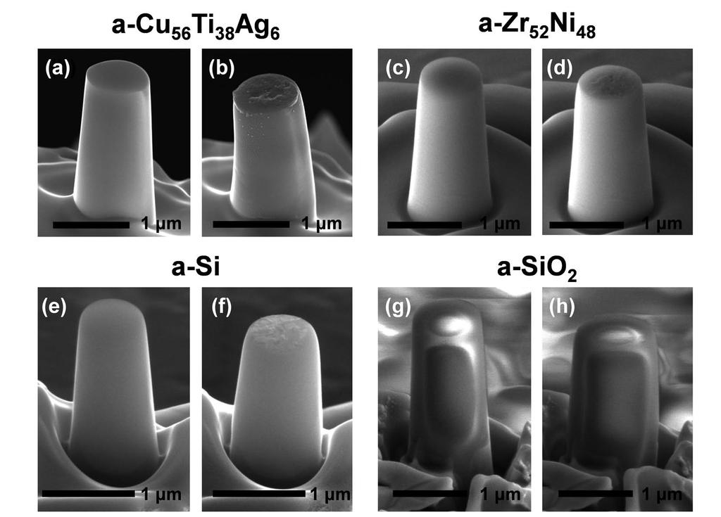
5 diffraction (SAED) analyses. Figure 2 shows the XRD data of a-cu 56 Ti 38 Ag 6, 29 a-zr 52 Ni 48 and a- SiO 2 samples before irradiation and SAED pattern of an a-si micropillar after irradiation. Inset of Fig. 2(d) shows literature data of a-sio 2 after 31. III. RESULTS Figure 3 shows SEM images of a-cu 56 Ti 38 Ag 6, 29 a-zr 52 Ni 48, a-si, and a-sio 2 micropillars before and after the creep test. Initial experiments with a-si samples resulted in bending of the micropillar, which was attributed to the inhomogeneous amorphization at the base region of the micropillar due to the large nonuniformity in the displacement damage at that location. The inhomogeneous amorphization was eliminated by placing a 1 μm thick platinum protection layer at the base of the micropillar, using focused ion beam-assisted chemical vapor deposition. The penetration depth of 1.8 MeV Ar + in platinum is 800 nm, 32 therefore the platinum layer completely shields the base of the micropillar from irradiation damage. No bending was observed in the a-si micropillars that had this protection layer; a similar protection layer was utilized for the a-sio 2 micropillars. The a-sio 2 micropillars were observed to become thinner along the ion beam direction following irradiation, presumably due to irradiation-induced anisotropic deformation. 8 In order to eliminate the uncertainties that would result from the compression of elongated micropillars, the pre-irradiation of the SiO 2 micropillars was limited to ions/cm 2, minimizing the change in shape. For all the ions used, this damage level is beyond the saturation dose required for the irradiation-induced densification of SiO 2, dpa. The other samples, a-cu 56 Ti 38 Ag 6, a- Zr 52 Ni 48 and a-si micropillars did not show any observable anisotropic deformation. 5
6 Figure 4 shows the deformation and strain of a-cu 56 Ti 38 Ag 6, 29 a-zr 52 Ni 48, a-si and a-sio 2 micropillars as a function of time and displacement damage. Each micropillar was loaded three times with different initial transducer deflections, resulting in different stress levels. In the intervals where no deformation is taking place, the micropillar is disengaged from the transducer, i.e., no loading, but there is irradiation. Thus, the measured deformation is not due to beam heating or some other artifact associated with the irradiation, per se. For each loading, the deformation increases approximately linearly with time, and the deformation rate is proportional to the applied stress. These are the consequences of the Newtonian nature of the IIC in amorphous materials, in agreement with previous findings. 2,8,33 Deformation jumps are seen at the onset of each loading; we attribute these artifacts to the combined effects of repositioning of the transducer after each engagement and the finite compliance of the frame of the apparatus. The IIC of an amorphous material under uniaxial stress can be described by d 1 H, (1) d 3 3 where ε is strain rate, φ is ion flux, σ is the applied stress, η is viscosity and H 1/ is the irradiation-induced fluidity. For point-defect mediated creep, it is more convenient to define H dpa 1/ dpa, where H dpa (Pa -1 dpa -1 ) is the fluidity normalized by the displacement damage rate, dpa (dpa/s), which is calculated using TRIM; 32 dpa refers to displacements per atom and is a normalized unit of dose. Figure 5 shows the measured strain rates normalized by dpa as a function of absolute value of the micropillar stress. The slopes of the data in these plots yield H dpa. Figure 5(a) shows our data for a-cu 56 Ti 38 Ag 6, 29 a-zr 52 Ni 48 and a-si, as well as literature values for: 6.3 MeV proton irradiated a-ni 78 B 14 Si 8, kev Kr + irradiated a-zr 65 Cu 27.5 Al 7.5, 10 and 800 kev Kr + irradiated a-zr 65 Cu The solid line is the prediction of a point defect model 34 6
7 which is described in the discussion section. The dashed line is a fit to the a-cu 56 Ti 38 Ag 6 and a- Zr 52 Ni 48 data, and the dotted line is a fit to the a-si data. For the stress relaxation measurements, 10 an average stress is used for locating the data point (assuming Newtonian flow) and biaxial strain rate is multiplied by two in order to obtain the corresponding uniaxial strain rate for comparison. Figure 5(b) shows our data for a-sio 2 bombarded by 1.8 MeV Ne +, Ar + and Kr +. Dashed lines are fits to the Ne + and Ar + data, and dotted line indicates the average of stress relaxation measurements for MeV Ne + and MeV Xe + irradiation on a-sio 2. 8 Several differences are observed in comparison to the other amorphous materials. First, the fluidities for the different ions no longer scale with dpa; the fluidities, moreover, tend to be greater than those for a-cu 56 Ti 38 Ag 6, a-zr 52 Ni 48 and a-si, except for the Kr + irradiation, which is similar to these in magnitude. Several measurements using stress relaxation have previously been performed on a- SiO ,11 These data representing various ions and energies (dotted line in Fig. 5(b)) all fall close to the line passing through our Kr + irradiation, and consequently they are also similar to the a-metals and a-si in Fig. 5(a). IV. DISCUSSION The irradiation-induced fluidities (IIF) in three very different types of amorphous materials: metallic glasses, a-si and a-sio 2, arising from nuclear stopping, are very nearly the same when normalized by dpa. While we have used dpa for normalization, we have chosen the same displacement energy for all materials, 10 ev, and so scaling with damage energy works equally well. By using dpa, however, comparison can be made directly with MD simulation and good agreement is obtained as discussed below. The damage energy is the total projectile energy less 7
8 that going into electronic excitation. Previous work using stress relaxation measurements showed that in a-sio 2, IIF scaled with the maximum nuclear stopping power of the projectile. 8 Indeed, several later studies using stress relaxation measurements also indicated this same behavior. 9,11 While those results are in good agreement with our results for 1.8 MeV Kr + irradiation of a-sio 2, they are not, at first glance, in agreement with our results using Ne + and Ar + irradiations. This is surprising, since the previous work included Ne + irradiation in the same energy range. 8 The present work shows, however, that the scaling of IIF in a-sio 2 with damage energy is an approximation that only holds when the electronic stopping power can be neglected. We discuss these findings in terms of current models of irradiation-induced fluidity and offer an explanation for the different results obtained using stress relaxation or micropillar creep experiments. We first discuss the thermal spike model of IIF by Trinkaus. 35 The Trinkaus model assumes that energy deposition during the slowing of an ion leads to local heating, and if the energy density is sufficiently high in these regions, the local temperature can rise above the glass temperature. Elastic relaxations around these thermal spikes then lead to permanent plastic deformation when the melt region refreezes The Trinkaus model distinguishes between spherical spikes and cylindrical spikes, although more important for the present work are the causes of the heat spikes. In metals and Si electronic excitation plays no significant role since the electronic system carries away the heat before it can effectively couple locally to the phonon system. It is only the energy transferred directly to the phonon systems that can cause local heating, i.e., nuclear stopping. Thermal spikes arising from nuclear stopping tend to be spherical. In insulators, electron excitations remain localized, eventually coupling to the phonon system. 40 Since the electron stopping is more or less continuous along the track of the ion, the thermal spike is cylindrical. 8
9 A second model of IIF due to nuclear stopping derives from molecular dynamics (MD) simulations by Mayr et al, 34 i.e., the point defect model. The point defect in this context refers to a Frenkel pair-like defect generated by the displacement of an atom from its local site to a new high energy interstitial site, leaving an excess volume, or vacancy behind. 34 Local relaxations around these defect sites are biased by an applied stress, and this leads to creep deformation. Such local relaxations are akin to shear transformation zones (STZ) in supercooled liquids, although under irradiation their concentration is determined by defect production rather than thermal excitations. The model differs from the thermal spike model in that spatial location of the defects, and therefore energy distribution in the solid, has no direct effect on IIF. Consequently, the near universality of IIF is naturally explained within this model, since the number of defects created scales with damage energy, i.e., the displacement energy for defect production does not greatly vary from one material to the next. 41 As shown in Fig. 5(a), this model agrees very well quantitatively with experiments, with H dpa 3 GPa -1 dpa -1. The defect model does not account for electronic excitation. Additional details of these models are not important for the current discussion and will not be provided here. The interested reader, however, is referred to refs 34,37. The total irradiation-induced fluidity can be estimated by H total = H e + H n where H e and H n are the fluidities due to electronic and nuclear stopping, respectively. We separate the contributions of nuclear and electronic excitation since the nuclear contribution is caused almost entirely by recoils while the electronic component results from the thermal spike along the track of the irradiation particle. Fluidity due to nuclear stopping will be taken as H dpa,n = 3 GPa -1 dpa -1 as determined by experiments (or the defect model). Since the spherical thermal spike regions and the displacement cascades leading to point defects mostly overlap, we ignore the 9
10 contribution from spherical thermal spikes to avoid relaxing the same volume twice. Fluidity due to electronic stopping can be estimated using the expression: 36 H e 3B SV e K (2) Q where K is the efficiency of the cylindrical spikes, μ is the shear modulus, B is a geometric factor, S e is the electronic stopping power excluding recoils, V is the volume that goes through stress relaxation per spike, and Q is the energy deposited per spike. For uniaxial loading perpendicular to the ion beam axis, 36 B 41 V / Q for the cylindrical spikes is given by the expression: 36 e where ν = 0.17 for a-sio 2. 9,42 The value of V 1 1 Q e C T T f 0 (3) where ρ is the density (2.23 g/cm 3 for a-sio 2 ), C is the specific heat capacity (1250 J/(kg K) 9,41 for a-sio 2 ), T f is the flow temperature (we use T f = 2000 K, in accordance with refs. 9,38 ), and T 0 is the temperature of the irradiated specimen (273 K). Below an electronic stopping power threshold, the energy deposited along the ion track does not induce effective thermal spikes that contribute to IIF in a-sio 2. Effective thermal spikes also result in anisotropic deformation, 7,43 which in fact were used to determine the threshold value. Van Dillen et al., 44 for example, have measured the dimensional changes of spherical silica colloids due to irradiation as a function of S e in the range kev/nm. Their data suggest a threshold value in the range kev/nm. Benyagoub et al., 45 on the other hand have suggested a value of 2 kev/nm. We use a threshold of 1 kev/nm for calculations below; this value is in the middle of the range of possible values. Therefore, the efficiency factor, K = 0 for S e < 1 kev/nm. Due to the presence of this threshold value, the electronic stopping along the paths of the relatively low-energy recoils does not contribute to the fluidity, therefore S e does not 10
11 include the stopping power from recoils in our calculations. For S e > 1 kev/nm, we take K = 0.21 following the experimental findings of Brongersma et al. 9 K being equal to unity corresponds to the limiting case where all of the electronic stopping power is spent on perfectly efficient cylindrical spikes. Figure 6(a) shows the electronic stopping and nuclear stopping power of ions as a function of depth into the sample for all three experimental conditions of a-sio 2 micropillars. The inset shows the same information for a-cu 56 Ti 38 Ag 6, a-zr 52 Ni 48, and a-si micropillars. Electronic stopping due to recoils is not included in the plot for the reasons noted above. As mentioned above, the IIF associated with nuclear stopping is known, and since it scales with dpa, we use such scaling for calculations discussed below. The vertical line indicates the average thickness of the 1 μm diameter micropillars as viewed by the ion beam. The electronic stopping decreases and the nuclear stopping increases as the ions penetrate through the micropillar specimen. For the ion energies and targets selected, nuclear stopping is higher and electronic stopping is lower for heavier ions. The horizontal line of 1 kev/nm is the estimated threshold electronic stopping power for efficient thermal spikes noted above. 44 For 1.8 MeV Kr + on a-sio 2, the electronic stopping is below the threshold value throughout the micropillar. We thus see why IIF for 1.8 MeV Kr + irradiated a-sio 2 is similar to a-metals and a-si. By using the information in Fig. 6(a), the irradiation-induced fluidity, H, due to each mechanism, and the total fluidity, H total = H e + H n can now be determined. As noted above for a- Cu 56 Ti 38 Ag 6, a-zr 52 Ni 48, and a-si, high electron mobility results in rapid dissipation of electronic excitations, therefore cylindrical spikes are not effective, H e 0. The lack of visible anisotropic deformation in these samples supports this assumption since anisotropic deformation takes place only due to cylindrical spikes and not due to spherical spikes
12 Before discussing the predicted irradiation-induced fluidity values in a-sio 2, we briefly comment on the effect of anisotropic deformation on the compression creep measurements. Anisotropic deformation refers to the change in shape of an amorphous material due to ion irradiation, and it arises from the cylindrical thermal spikes. It results in shrinkage in the direction parallel to the path of the projectile and expansion normal to it. The governing equation that relates the irradiation-induced creep and the anisotropic deformation is given by, 46 d dt ij 1 d Hij 1 ij kk ij Aij ij kk ij 2G dt (4) where ε ij is the strain tensor, σ ij is the stress tensor, G is the shear modulus, ν is Poisson s ratio, δ ij is Kronecker delta, A ij is the anisotropic deformation tensor, and H ij is the fluidity tensor. For the constant applied stress in these experiments, the first term can be neglected. The anisotropic deformation is linearly related to the electronic stopping power 11 and one can write e threshold A c S S (5) where c = m 2 nm/ev 11 and we take S threshold as 1 kev/nm. Considering the case of the most pronounced anisotropic deformation, 1.8 MeV Ne + on a-sio 2, S e = 1.2 kev/nm, averaged over the thickness of the micropillar, and A = m 2 /ion. The lowest stress applied in our measurements is σ 50 MPa, and corresponding normalized strain rate, = m 2 /ion. Therefore, for the parameters of the current experiment, the irradiation-induced creep dominates over anisotropic deformation during loading, and therefore we neglect the effect of anisotropic deformation in these creep measurements. Figure 6(b) shows the irradiation-induced fluidity due to cylindrical spikes (H e ) and from point defect creation (H n ), and the total value (H total ) as a function of sample depth for the a-sio 2 micropillars. The same information is shown in the inset for a-cu 56 Ti 38 Ag 6, a-zr 52 Ni 48, and a-si. 12
13 For a-cu 56 Ti 38 Ag 6, a-zr 52 Ni 48, and a-si, H total increases towards the backside of the micropillar, being proportional to the nuclear stopping (see Fig. 6(a)). a-si has higher H in comparison to a- Cu 56 Ti 38 Ag 6 and a-zr 52 Ni 48 due to the higher displacement damage per ion fluence. The trends for a-sio 2 are more complex due to opposing variations of nuclear and electronic stopping with the atomic weight of the bombarding ion. In the range nm (the thickness of the micropillar), electronic stopping of 1.8 MeV Ar + is 10% smaller than that for 1.8 MeV Ne +, whereas Ar + has a larger H n. Therefore, H total is nearly the same for Ne + and Ar +. In either case, however, the variation of H total is dominated by electronic stopping, which decreases with depth and falls below the threshold toward the backside of the micropillar. For 1.8 MeV Kr +, the electronic stopping power never rises above the threshold (see Fig. 6(a)), so for it, H e 0. On the other hand, H n is very high due to the large nuclear stopping power, and it acts toward balancing the loss of H e contribution. Since H total = H n for Kr + bombardment, it increases toward the backside of the micropillar. An important aspect of the present irradiation-induced creep measurements is the effect of the inhomogeneity of the fluidity across the thickness of the specimen. In our previous work, 29 we have shown through finite element analysis that even for a damage variation on the order of 50%, the measured creep rate is within 30% of the hypothetical case of uniform damage for total strains up to 10%. This is due to the increased stress in the low fluidity regions of the micropillar which acts towards balancing the damage inhomogeneity through Newtonian flow. Table I shows a summary of H values averaged over the thickness of the specimen using the information in Fig. 6(b). The comparison between the predicted total fluidity, H total, and measured fluidity H exp shows very good agreement between model predictions and experimental data. The agreement for a-cu 56 Ti 38 Ag 6, a-zr 52 Ni 48, a-si, and 1.8 MeV Kr + bombarded a-sio 2 13
14 shows the accuracy of the point defect model by Mayr et al. 34 whereas the agreement for 1.8 MeV Ne + provides evidence about the validity of the Trinkaus model for electronic stopping. 36 It is interesting to note that the predicted fluidity, H total (in units of m 2 /(Pa ion)) remains almost the same for a-sio 2 from Ne + through Kr + bombardment due to the two different mechanisms balancing each other. We note that the irradiation-induced fluidity for 1.8 MeV Ar + on a-sio 2 is somewhat larger than the theoretical estimate, for which we have no firm explanation. The deviation appears somewhat too large to be experimental error, or an effect on inhomogeneous damage. Possibly the difference derives from synergistic effects between the electronic and nuclear stopping. For Ne +, nuclear stopping is very small, whereas for Kr +, the electronic stopping is below the threshold. Therefore, Ar + is the only ion that has significant contribution from both effects, and in the regions where the cylindrical and spherical spikes overlap, the stress relaxation might be more efficient. For example MD simulations indicate that IIF in the point defect model increases by about a factor of three when the irradiation temperature is raised from 100 K to 400 K, 34 and so the thermal spike from electronic stopping may enhance the effect of point defects. Additional work will be necessary to clarify this point. Lastly we comment why previous work on IIF of a-sio 2 found that their experimental measurements could be fit very well by scaling IIF to nuclear stopping, without a contribution of electronic stopping. We believe the answer derives from using stress relaxation measurements where only the average stress in the sample is measured over the entire penetration depth of the ion. Since the ions in these experiments are stopped within the sample, it tends to diminish the role of the electronic excitation and increase that of the nuclear stopping. In the micropillar experiments, the projectile passes through the sample, diminishing the effect of the end of range damage, thus enhancing the effect of electronic excitation. This is seen in Fig. 6 which shows 14
15 that the average nuclear stopping (and H n ) for given ion and energy is much smaller for the 1 μm-diameter micropillar compression case than the stress relaxation case. On the other hand, for Ne + and Ar + irradiation, the electronic stopping is less effective for stress relaxation case since the stopping power is below the threshold for most of the thickness of the irradiated region. IV. CONCLUSIONS We have performed a comparative experimental analysis of irradiation-induced creep in a variety of amorphous materials with different types of bonding, using the same specimen geometry and testing conditions. The results show strong support for the point defect model of plastic flow in a-cu 56 Ti 38 Ag 6, a-zr 52 Ni 48 and a-si, in agreement with the predictions. 34 The model also works well for IIF in a-sio 2, when electronic excitation is not too large. In general, however, IIF is larger in a-sio 2 than in the other amorphous materials studied here, owing to stress relaxation in cylindrical thermal spikes along the track of the irradiation particle. 36 This is important, however, only when electronic stopping power exceeds 1 kev/nm. ACKNOWLEDGEMENTS This research was supported by the U.S. Department of Energy, Office of Basic Energy Sciences, Division of Materials Sciences and Engineering under Award DEFG02-05ER The work was carried out, in part, in the Frederick Seitz Materials Research Laboratory Central Facilities, University of Illinois. We thank Dr. M. T. Saif for useful discussions and S. Mao for TEM analysis of the Si micropillars. 15
16 TABLES TABLE I. Average stopping power, and theoretical and experimental values of irradiationinduced fluidity. 2.1 MeV Ne + on 29 a-cu 56 Ti 38 Ag MeV Ne + on a- Zr 52 Ni MeV Ar + on a-si 1.8 MeV Ne + on a-sio MeV Ar + on a-sio MeV Kr + on a-sio 2 S e S n H e H (m 2 /(Pa ion)) b H n H total H exp σ H,exp c H dpa,exp (GPa -1 dpa -1 ) a Stopping power. Subscripts e and n correspond to electronic and nuclear, respectively. b Irradiation-induced fluidity. c Standard deviation of the measured irradiation-induced fluidity. 16
17 FIGURE CAPTIONS FIG. 1. (color online) Schematic view of the measurement procedure. 29 (a) Micropillar is disengaged from the transducer. (b) Nanopositioner moves the micropillar up, deflecting the transducer. Micropillar is now under load and ion bombardment. (c) Micropillar deforms, resulting transducer deflection to decrease. (d) SEM image of a microfabricated doubly clamped silicon beam transducer. 29 The cylindrical punch region at the center of the beam facilitates micropillar alignment. FIG. 2. (color online) XRD data of a-cu 56 Ti 38 Ag 6, 29 a-zr 52 Ni 48, and a-sio 2 samples before irradiation, and SAED pattern of an a-si micropillar after irradiation, indicating amorphous structure. In (d), the data correspond to the difference between the data of the a-sio 2 sample on Si substrate and the data of a single crystal Si sample. Inset of (d) shows literature data of a-sio 2 after 31. FIG. 3. SEM images of the micropillar specimens. (a) a-cu 56 Ti 38 Ag 6 before and (b) after the creep test, 29 (c) a-zr 52 Ni 48 before and (d) after the creep test, (e) a-si before and (f) after the creep test, (g) a-sio 2 before and (h) after the creep test. FIG. 4. (color online) Deformation (strain) of the micropillars as a function of time (displacement damage). Each micropillar is loaded three times with the indicated stress level in MPa. Regions of zero slope are when the micropillar is disengaged from the transducer. FIG. 5. (color online) Normalized strain rate as a function of absolute value of micropillar stress. Filled markers are the results of the present study and previous a-cu 56 Ti 38 Ag 6 data, 29 and hollow markers are literature values. In (a), the solid line indicates the theoretical prediction, 34 the dashed line is a fit to the a-cu 56 Ti 38 Ag 29 6 and a-zr 52 Ni 48 data, and the dotted line is a fit to the a-si data. In (b), dashed lines are fits to the Ne + and Ar + irradiated a-sio 2 data, and the dotted 17
18 line is the average of stress relaxation measurements for MeV Ne + and MeV Xe + irradiation on a-sio 2. 8 FIG. 6. (color online) (a) Electronic and nuclear stopping power as a function of depth into the samples for 1.8 MeV Ne +, Ar + and Kr + bombardment on a-sio 2. Inset shows the same information for 2.1 MeV Ne + on a-cu 56 Ti 38 Ag 6, 2.0 MeV Ne + on a-zr 52 Ni 48 and 1.8 MeV Ar + on a-si. Electronic stopping excludes the contribution from recoils. The horizontal dashed line indicates the threshold value for efficient cylindrical spikes, and the vertical lines indicate the thickness of the micropillar specimens. (b) Irradiation-induced fluidity as a function of depth into the a-sio 2 samples. Inset shows the same information for a-cu 56 Ti 38 Ag 6, a-zr 52 Ni 48 and a-si. Fluidities due to electronic stopping, due to point defects, and the total values are shown. Inset only shows total fluidities, which is equal to H n. 18
 250 μm FIG. 1.")
19 FIGURES laser sensor reference position (a) (b) (c) transducer center transducer deflection of loading micropillar deformation ion beam micropillar nanopositioner nanopositioner motion (d) 250 μm FIG
20 (a) 750 a-cu 56 Ti 38 Ag 6 Cu(111) Cu(220) Ag(311) Counts Ti(101) (b) log(counts) (d) Relative counts Ag(111) Cu(200) a-zr Ni 48 (c) a-si Zr(101) Ni(111) 4.0 Zr(100) 3.0 Zr(002) 2.0 Si(400) a-sio Counts FIG

")
 (d) 1")

")
 1")


21 a-cu 56 Ti 38 Ag 6 a-zr 52 Ni 48 (a) (b) (b) (c) (d) 1 μm 1 μm 1 μm 1 μm a-si a-sio 2 (e) (f) (g) (h) 1 μm 1 μm 1 μm 1 μm FIG

22 FIG
23 (a) (dpa -1 ) Theory 3 dpa -1 GPa MeV Ar + on a-si (b) MeV Ne + on a-zr 52 Ni MeV proton on Ni 78 B 14 Si kev Kr + on Zr 65 Cu 27.5 Al kev Kr + on Zr 65 Cu a-sio MeV Ne + on a-cu 56 Ti 38 Ag 6 15 (dpa-1 ) MeV Ne + 83 dpa -1 GPa MeV Ar + 35 dpa -1 GPa MeV Kr dpa -1 GPa Stress (MPa) FIG

24 FIG
25 REFERENCES 1 W. Primak, J. Appl. Phys. 53, 7331 (1982). 2 C.A. Volkert, J. Appl. Phys. 70, 3521 (1991). 3 C.A. Volkert and A. Polman, MRS Proc. 235, 3 (1991). 4 P.D. Townsend, Nucl. Instrum. Methods Phys. Res. Sect. B Beam Interact. Mater. At. 46, 18 (1990). 5 M.V. Rao, IEEE Trans. Electron Devices 40, 1053 (1993). 6 P. Jung, J. Appl. Phys. 86, 4876 (1999). 7 E. Snoeks, A. Polman, and C.A. Volkert, Appl. Phys. Lett. 65, 2487 (1994). 8 E. Snoeks, T. Weber, A. Cacciato, and A. Polman, J. Appl. Phys. 78, 4723 (1995). 9 M.L. Brongersma, E. Snoeks, and A. Polman, Appl. Phys. Lett. 71, 1628 (1997). 10 S.G. Mayr and R.S. Averback, Phys. Rev. B 68, (2003). 11 T. van Dillen, M.Y.S. Siem, and A. Polman, Appl. Phys. Lett. 85, 389 (2004). 12 P.L. Hendrick, D.J. Michel, A.G. Pieper, R.E. Surratt, and A.L. Bement Jr., J. Nucl. Mater. 59, 229 (1976). 13 P. Blanchard, P. Jary, and J. Delaplace, J. Nucl. Mater. 74, 267 (1978). 14 P.L. Hendrick, Nucl. Instrum. Methods 161, 345 (1979). 15 P. Jung, C. Schwaiger, and H. Ullmaier, J. Nucl. Mater , 867 (1979). 16 T.C. Reiley, R.L. Auble, and R.H. Shannon, J. Nucl. Mater. 90, 271 (1980). 17 S.K. Khera, C. Schwaiger, and H. Ullmaier, J. Nucl. Mater. 92, 299 (1980). 18 C. Xu and G.S. Was, J. Nucl. Mater. 441, 681 (2013). 19 J.A. Hudson, R.S. Nelson, and R.J. McElroy, J. Nucl. Mater. 65, 279 (1977). 20 E.K. Opperman, J.L. Straalsund, G.L. Wire, and R.H. Howell, Nucl Technol 42, 71 (1979). 21 Z. Zhu and P. Jung, Nucl. Instrum. Methods Phys. Res. Sect. B Beam Interact. Mater. At. 91, 269 (1994). 22 P. Jung, A. Schwarz, and H.K. Sahu, Nucl. Instrum. Methods Phys. Res. Sect. A 234, 331 (1985). 23 S. Hirsch, H. Klein, and P. Jung, J. Non-Cryst. Solids 351, 3279 (2005). 24 J. Nagakawa, S. Uchio, Y. Murase, N. Yamamoto, and K. Shiba, J. Nucl. Mater , 264 (2009). 25 A. Audouard, E. Balanzat, J.C. Jousset, G. Fuchs, D. Lesueur, and L. Thomé, Nucl. Instrum. Methods Phys. Res. Sect. B Beam Interact. Mater. At. 39, 18 (1989). 26 A. Barbu, M. Bibole, R. Le Hazif, S. Bouffard, and J.C. Ramillon, J. Nucl. Mater. 165, 217 (1989). 27 K. Tai, R.S. Averback, P. Bellon, and Y. Ashkenazy, Scr. Mater. 65, 163 (2011). 28 K. Tai, R.S. Averback, P. Bellon, Y. Ashkenazy, and B. Stumphy, J. Nucl. Mater. 422, 8 (2012). 29 S. Özerinç, R.S. Averback, and W.P. King, J. Nucl. Mater. 451, 104 (2014). 30 D.N. Seidman, R.S. Averback, P.R. Okamoto, and A.C. Baily, Phys. Rev. Lett. 58, 900 (1987). 31 Y. Fujimoto, in Advances in Solid State Lasers Development and Applications, ed. M. Grishin (InTech, 2010). 32 J.F. Ziegler, J.P. Biersack, and M.D. Ziegler, SRIM, the Stopping and Range of Ions in Matter (SRIM Co., Chester, Maryland, 2008). 33 S.G. Mayr and R.S. Averback, Phys. Rev. Lett. 87, (2001). 34 S.G. Mayr, Y. Ashkenazy, K. Albe, and R.S. Averback, Phys. Rev. Lett. 90, (2003). 25
26 35 H. Trinkaus and A.I. Ryazanov, Phys. Rev. Lett. 74, 5072 (1995). 36 H. Trinkaus, J. Nucl. Mater. 223, 196 (1995). 37 H. Trinkaus, Nucl. Instrum. Methods Phys. Res. Sect. B Beam Interact. Mater. At. 107, 155 (1996). 38 H. Trinkaus, J. Nucl. Mater. 246, 244 (1997). 39 H. Trinkaus, Nucl. Instrum. Methods Phys. Res. Sect. B Beam Interact. Mater. At. 146, 204 (1998). 40 M. Toulemonde, J.M. Costantini, C. Dufour, A. Meftah, E. Paumier, and F. Studer, Nucl. Instrum. Methods Phys. Res. Sect. B Beam Interact. Mater. At. 116, 37 (1996). 41 G.S. Was, Fundamentals of Radiation Materials Science Metals and Alloys (Springer, Berlin, 2007). 42 H. Scholze, Glass: Nature, Structure, and Properties (Springer-Verlag, New York, 1991). 43 S. Klaumünzer, L. Changlin, S. Löffler, M. Rammensee, and G. Schumacher, Nucl. Instrum. Methods Phys. Res. Sect. B Beam Interact. Mater. At. 39, 665 (1989). 44 T. van Dillen, A. Polman, W. Fukarek, and A. van Blaaderen, Appl. Phys. Lett. 78, 910 (2001). 45 A. Benyagoub, S. Löffler, M. Rammensee, S. Klaumünzer, and G. Saemann-Ischenko, Nucl. Instrum. Methods Phys. Res. Sect. B Beam Interact. Mater. At. 65, 228 (1992). 46 A. Gutzmann, S. Klaumünzer, and P. Meier, Phys. Rev. Lett. 74, 2256 (1995). 26

27

28
29
30
31
32
Interaction of ion beams with matter
 Interaction of ion beams with matter Introduction Nuclear and electronic energy loss Radiation damage process Displacements by nuclear stopping Defects by electronic energy loss Defect-free irradiation
, MgAl 2. and MgO irradiated with high energy heavy ions O 3
 Surface defects in Al 2, MgAl 2 O 4 and MgO irradiated with high energy heavy ions V.A.Skuratov 1, S.J. Zinkle 2 A.E.Efimov 1, K.Havancsak 3 1 Flerov Laboratory of Nuclear Reactions, JINR, Dubna, Russia
Chapter 4. Surface defects created by kev Xe ion irradiation on Ge
 81 Chapter 4 Surface defects created by kev Xe ion irradiation on Ge 4.1. Introduction As high energy ions penetrate into a solid, those ions can deposit kinetic energy in two processes: electronic excitation
Determining thermal noise limiting properties of thin films
 Determining thermal noise limiting properties of thin films Courtney Linn Institute for Gravitational Research University of Glasgow Summer 2011 Abstract In order to make thermally stable mirrors to be
Imaging Methods: Scanning Force Microscopy (SFM / AFM)
") Imaging Methods: Scanning Force Microscopy (SFM / AFM) The atomic force microscope (AFM) probes the surface of a sample with a sharp tip, a couple of microns long and often less than 100 Å in diameter.
Imaging Methods: Scanning Force Microscopy (SFM / AFM) The atomic force microscope (AFM) probes the surface of a sample with a sharp tip, a couple of microns long and often less than 100 Å in diameter.
SUPPLEMENTARY NOTES Supplementary Note 1: Fabrication of Scanning Thermal Microscopy Probes
 SUPPLEMENTARY NOTES Supplementary Note 1: Fabrication of Scanning Thermal Microscopy Probes Fabrication of the scanning thermal microscopy (SThM) probes is summarized in Supplementary Fig. 1 and proceeds
TMT4320 Nanomaterials November 10 th, Thin films by physical/chemical methods (From chapter 24 and 25)
") 1 TMT4320 Nanomaterials November 10 th, 2015 Thin films by physical/chemical methods (From chapter 24 and 25) 2 Thin films by physical/chemical methods Vapor-phase growth (compared to liquid-phase growth)
1 TMT4320 Nanomaterials November 10 th, 2015 Thin films by physical/chemical methods (From chapter 24 and 25) 2 Thin films by physical/chemical methods Vapor-phase growth (compared to liquid-phase growth)
Swift heavy ion irradiation effect on the surface of sapphire single crystals
 1 Radiation Measurements 34, 571 (2001). Swift heavy ion irradiation effect on the surface of sapphire single crystals V.A.Skuratov a, D.L.Zagorski b *, A.E.Efimov a, V.A.Kluev c, Yu.P.Toporov c, B.V.
Experience with Moving from Dpa to Changes in Materials Properties
 Experience with Moving from Dpa to Changes in Materials Properties Meimei Li, Argonne National Laboratory N. V. Mokhov, Fermilab 46 th ICFA Advanced Beam Dynamics Workshop Sept. 27 Oct. 1, 2010 Morschach,
Comparisons of DFT-MD, TB- MD and classical MD calculations of radiation damage and plasmawallinteractions
 CMS Comparisons of DFT-MD, TB- MD and classical MD calculations of radiation damage and plasmawallinteractions Kai Nordlund Department of Physics and Helsinki Institute of Physics University of Helsinki,
EE C247B / ME C218 INTRODUCTION TO MEMS DESIGN SPRING 2014 C. Nguyen PROBLEM SET #4
 Issued: Wednesday, Mar. 5, 2014 PROBLEM SET #4 Due (at 9 a.m.): Tuesday Mar. 18, 2014, in the EE C247B HW box near 125 Cory. 1. Suppose you would like to fabricate the suspended cross beam structure below
Modeling the Dynamic Propagation of Shear Bands in Bulk Metallic Glasses
 Modeling the Dynamic Propagation of Shear Bands in Bulk Metallic Glasses B.J. Edwards, K. Feigl, M.L. Morrison*, B. Yang*, P.K. Liaw*, and R.A. Buchanan* Dept. of Chemical Engineering, The University of
Mechanism of Elongation of Gold or Silver Nanoparticles in Silica by Irradiation with Swift Heavy Ions
 Mechanism of Elongation of Gold or Silver Nanoparticles in Silica by Irradiation with Swift Heavy Ions K. Awazu, X. Wang, M. Fujimaki, J. Tominaga, S. Fujii, H. Aiba, Y. Ohki, T. Komatsubara To cite this
Gaetano L Episcopo. Scanning Electron Microscopy Focus Ion Beam and. Pulsed Plasma Deposition
 Gaetano L Episcopo Scanning Electron Microscopy Focus Ion Beam and Pulsed Plasma Deposition Hystorical background Scientific discoveries 1897: J. Thomson discovers the electron. 1924: L. de Broglie propose
Metal Deposition. Filament Evaporation E-beam Evaporation Sputter Deposition
 Metal Deposition Filament Evaporation E-beam Evaporation Sputter Deposition 1 Filament evaporation metals are raised to their melting point by resistive heating under vacuum metal pellets are placed on
Chapter 4. The Effect of Elastic Softening and Cooperativity on the Fragility of
 Chapter 4 The Effect of Elastic Softening and Cooperativity on the Fragility of Glass-Forming Metallic Liquids Key words: Amorphous metals, Shear transformation zones, Ultrasonic measurement, Compression
Ion Implantation ECE723
 Ion Implantation Topic covered: Process and Advantages of Ion Implantation Ion Distribution and Removal of Lattice Damage Simulation of Ion Implantation Range of Implanted Ions Ion Implantation is the
Nanopore sculpting with noble gas ions
 JOURNAL OF APPLIED PHYSICS 100, 024914 2006 Nanopore sculpting with noble gas ions Qun Cai, a Brad Ledden, and Eric Krueger Department of Physics, University of Arkansas, Fayetteville, Arkansas 72701 Jene
MS482 Materials Characterization ( 재료분석 ) Lecture Note 5: RBS
 Lecture Note 5: RBS") 2016 Fall Semester MS482 Materials Characterization ( 재료분석 ) Lecture Note 5: RBS Byungha Shin Dept. of MSE, KAIST 1 Course Information Syllabus 1. Overview of various characterization techniques (1 lecture)
2016 Fall Semester MS482 Materials Characterization ( 재료분석 ) Lecture Note 5: RBS Byungha Shin Dept. of MSE, KAIST 1 Course Information Syllabus 1. Overview of various characterization techniques (1 lecture)
Intensity (a.u.) Intensity (a.u.) Raman Shift (cm -1 ) Oxygen plasma. 6 cm. 9 cm. 1mm. Single-layer graphene sheet. 10mm. 14 cm
 Intensity (a.u.) Raman Shift (cm -1 ) Oxygen plasma. 6 cm. 9 cm. 1mm. Single-layer graphene sheet. 10mm. 14 cm") Intensity (a.u.) Intensity (a.u.) a Oxygen plasma b 6 cm 1mm 10mm Single-layer graphene sheet 14 cm 9 cm Flipped Si/SiO 2 Patterned chip Plasma-cleaned glass slides c d After 1 sec normal Oxygen plasma
Intensity (a.u.) Intensity (a.u.) a Oxygen plasma b 6 cm 1mm 10mm Single-layer graphene sheet 14 cm 9 cm Flipped Si/SiO 2 Patterned chip Plasma-cleaned glass slides c d After 1 sec normal Oxygen plasma
6.4 A cylindrical specimen of a titanium alloy having an elastic modulus of 107 GPa ( psi) and
 and") 6.4 A cylindrical specimen of a titanium alloy having an elastic modulus of 107 GPa (15.5 10 6 psi) and an original diameter of 3.8 mm (0.15 in.) will experience only elastic deformation when a tensile
6.4 A cylindrical specimen of a titanium alloy having an elastic modulus of 107 GPa (15.5 10 6 psi) and an original diameter of 3.8 mm (0.15 in.) will experience only elastic deformation when a tensile
Implantation Energy Dependence on Deuterium Retention Behaviors for the Carbon Implanted Tungsten
 J. Plasma Fusion Res. SERIES, Vol. 10 (2013) Implantation Energy Dependence on Deuterium Retention Behaviors for the Carbon Implanted Tungsten Yasuhisa Oya 1) *, Makoto Kobayashi 1), Naoaki Yoshida 2),
Auger Electron Spectroscopy (AES)
") 1. Introduction Auger Electron Spectroscopy (AES) Silvia Natividad, Gabriel Gonzalez and Arena Holguin Auger Electron Spectroscopy (Auger spectroscopy or AES) was developed in the late 1960's, deriving
1. Introduction Auger Electron Spectroscopy (AES) Silvia Natividad, Gabriel Gonzalez and Arena Holguin Auger Electron Spectroscopy (Auger spectroscopy or AES) was developed in the late 1960's, deriving
Supplementary Figures
 Fracture Strength (GPa) Supplementary Figures a b 10 R=0.88 mm 1 0.1 Gordon et al Zhu et al Tang et al im et al 5 7 6 4 This work 5 50 500 Si Nanowire Diameter (nm) Supplementary Figure 1: (a) TEM image
Ion Implantation. alternative to diffusion for the introduction of dopants essentially a physical process, rather than chemical advantages:
 Ion Implantation alternative to diffusion for the introduction of dopants essentially a physical process, rather than chemical advantages: mass separation allows wide varies of dopants dose control: diffusion
EE 527 MICROFABRICATION. Lecture 24 Tai-Chang Chen University of Washington
 EE 527 MICROFABRICATION Lecture 24 Tai-Chang Chen University of Washington EDP ETCHING OF SILICON - 1 Ethylene Diamine Pyrocatechol Anisotropy: (100):(111) ~ 35:1 EDP is very corrosive, very carcinogenic,
Johns Hopkins University What is Engineering? M. Karweit MATERIALS
 Why do things break? Why are some materials stronger than others? Why is steel tough? Why is glass brittle? What is toughness? strength? brittleness? Elemental material atoms: MATERIALS A. Composition
Bending Load & Calibration Module
 Bending Load & Calibration Module Objectives After completing this module, students shall be able to: 1) Conduct laboratory work to validate beam bending stress equations. 2) Develop an understanding of
Lab1. Resolution and Throughput of Ion Beam Lithography.
 1 ENS/PHY463 Lab1. Resolution and Throughput of Ion Beam Lithography. (SRIM 2008/2013 computer simulation) Objective The objective of this laboratory work is to evaluate the exposure depth, resolution,
MATERIALS. Why do things break? Why are some materials stronger than others? Why is steel tough? Why is glass brittle?
 MATERIALS Why do things break? Why are some materials stronger than others? Why is steel tough? Why is glass brittle? What is toughness? strength? brittleness? Elemental material atoms: A. Composition
NITROGEN CONTAINING ULTRA THIN SiO 2 FILMS ON Si OBTAINED BY ION IMPLANTATION
 NITROGEN CONTAINING ULTRA THIN SiO 2 FILMS ON Si OBTAINED BY ION IMPLANTATION Sashka Petrova Alexandrova 1, Evgenia Petrova Valcheva 2, Rumen Georgiev Kobilarov 1 1 Department of Applied Physics, Technical
DEPOSITION OF THIN TiO 2 FILMS BY DC MAGNETRON SPUTTERING METHOD
 Chapter 4 DEPOSITION OF THIN TiO 2 FILMS BY DC MAGNETRON SPUTTERING METHOD 4.1 INTRODUCTION Sputter deposition process is another old technique being used in modern semiconductor industries. Sputtering
Creation and annealing of point defects in germanium crystal lattices by subthreshold energy events
 Creation and annealing of point defects in germanium crystal lattices by subthreshold energy events University of Sevilla 203 Sergio M. M. Coelho, Juan F. R. Archilla 2 and F. Danie Auret Physics Department,
MS482 Materials Characterization ( 재료분석 ) Lecture Note 5: RBS. Byungha Shin Dept. of MSE, KAIST
 Lecture Note 5: RBS. Byungha Shin Dept. of MSE, KAIST") 2015 Fall Semester MS482 Materials Characterization ( 재료분석 ) Lecture Note 5: RBS Byungha Shin Dept. of MSE, KAIST 1 Course Information Syllabus 1. Overview of various characterization techniques (1 lecture)
2015 Fall Semester MS482 Materials Characterization ( 재료분석 ) Lecture Note 5: RBS Byungha Shin Dept. of MSE, KAIST 1 Course Information Syllabus 1. Overview of various characterization techniques (1 lecture)
Relaxation of a Strained Elastic Film on a Viscous Layer
 Mat. Res. Soc. Symp. Proc. Vol. 695 Materials Research Society Relaxation of a Strained Elastic Film on a Viscous Layer R. Huang 1, H. Yin, J. Liang 3, K. D. Hobart 4, J. C. Sturm, and Z. Suo 3 1 Department
SUPPLEMENTARY INFORMATION
 Supplementary Information for Manuscript: Nanoscale wear as a stress-assisted chemical reaction Supplementary Methods For each wear increment, the diamond indenter was slid laterally relative to the silicon
Irradiation Behaviors of Nuclear Grade Graphite in Commercial Reactor, (II)
") Journal of NUCLEAR SCIENCE and TECHNOLOGY, 22[3J, pp. 225-232 (March 1985). 225 TECHNICAL REPORT Irradiation Behaviors of Nuclear Grade Graphite in Commercial Reactor, (II) Thermal and Physical Properties
Journal of NUCLEAR SCIENCE and TECHNOLOGY, 22[3J, pp. 225-232 (March 1985). 225 TECHNICAL REPORT Irradiation Behaviors of Nuclear Grade Graphite in Commercial Reactor, (II) Thermal and Physical Properties
Low Energy Nuclear Fusion Reactions in Solids
 Kasagi, J., et al. Low Energy Nuclear Fusion Reactions in Solids. in 8th International Conference on Cold Fusion. 2000. Lerici (La Spezia), Italy: Italian Physical Society, Bologna, Italy. Low Energy Nuclear
MULTIPACTOR ON A DIELECTRIC SURFACE WITH LONGITUDINAL RF ELECTRIC FIELD ACTION
 Progress In Electromagnetics Research Letters, Vol. 24, 177 185, 211 MULTIPACTOR ON A DIELECTRIC SURFACE WITH LONGITUDINAL RF ELECTRIC FIELD ACTION F. Zhu *, Z. Zhang, J. Luo, and S. Dai Key Laboratory
In situ TEM studies of helium bubble/platelet evolution in Si based materials
 In situ TEM studies of helium bubble/platelet evolution in Si based materials M. Vallet 1, M.F. Beaufort 1, J.F. Barbot 1, E. Oliviero 2 and S.E. Donnelly 3 1 Institut Pprime, CNRS-Université de Poitiers,
Radioactivity - Radionuclides - Radiation
 Content of the lecture Introduction Particle/ion-atom atom interactions - basic processes on on energy loss - stopping power, range Implementation in in Nucleonica TM TM Examples Origin and use of particles
Improvement of depth resolution of VEPAS by a sputtering technique
 Martin Luther University Halle Improvement of depth resolution of VEPAS by a sputtering technique R. Krause Rehberg, M. John, R. Böttger, W. Anwand and A. Wagner Martin Luther University Halle & HZDR Dresden
Investigations of the effects of 7 TeV proton beams on LHC collimator materials and other materials to be used in the LHC
 Russian Research Center Kurchatov Institute Investigations of the effects of 7 ev proton beams on LHC collimator materials and other materials to be used in the LHC A.I.Ryazanov Aims of Investigations:
Stress-Strain Behavior
 Stress-Strain Behavior 6.3 A specimen of aluminum having a rectangular cross section 10 mm 1.7 mm (0.4 in. 0.5 in.) is pulled in tension with 35,500 N (8000 lb f ) force, producing only elastic deformation.
Determining the Elastic Modulus and Hardness of an Ultrathin Film on a Substrate Using Nanoindentation
 Determining the Elastic Modulus and Hardness of an Ultrathin Film on a Substrate Using Nanoindentation The Harvard community has made this article openly available. Please share how this access benefits
PIEZOELECTRIC TECHNOLOGY PRIMER
 PIEZOELECTRIC TECHNOLOGY PRIMER James R. Phillips Sr. Member of Technical Staff CTS Wireless Components 4800 Alameda Blvd. N.E. Albuquerque, New Mexico 87113 Piezoelectricity The piezoelectric effect is
Stress generation mechanisms in carbon thin films grown by ion-beam deposition
 Acta Materialia 51 (2003) 5211 5222 www.actamat-journals.com Stress generation mechanisms in carbon thin films grown by ion-beam deposition Sulin Zhang a,, Harley T. Johnson b, Gregory J. Wagner c, Wing
3.032 Problem Set 2 Solutions Fall 2007 Due: Start of Lecture,
 3.032 Problem Set 2 Solutions Fall 2007 Due: Start of Lecture, 09.21.07 1. In the beam considered in PS1, steel beams carried the distributed weight of the rooms above. To reduce stress on the beam, it
3.032 Problem Set 4 Fall 2007 Due: Start of Lecture,
 3.032 Problem Set 4 Fall 2007 Due: Start of Lecture, 10.19.07 1. A microelectronic sensor is to be made of conductive wires deposited on a thin Si wafer. During design considerations, it was decided that
Chapiter VII: Ionization chamber
 Chapiter VII: Ionization chamber 1 Types of ionization chambers Sensitive volume: gas (most often air direct measurement of exposure) ionization chamber Sensitive volume: semiconductor (silicon, germanium,
EE C247B / ME C218 INTRODUCTION TO MEMS DESIGN SPRING 2016 C. NGUYEN PROBLEM SET #4
 Issued: Wednesday, March 4, 2016 PROBLEM SET #4 Due: Monday, March 14, 2016, 8:00 a.m. in the EE C247B homework box near 125 Cory. 1. This problem considers bending of a simple cantilever and several methods
DEVELOPMENT OF A NEW POSITRON LIFETIME SPECTROSCOPY TECHNIQUE FOR DEFECT CHARACTERIZATION IN THICK MATERIALS
 Copyright JCPDS - International Centre for Diffraction Data 2004, Advances in X-ray Analysis, Volume 47. 59 DEVELOPMENT OF A NEW POSITRON LIFETIME SPECTROSCOPY TECHNIQUE FOR DEFECT CHARACTERIZATION IN
Very large plasmon band shift in strongly coupled metal nanoparticle chain arrays.
 Mat. Res. Soc. Symp. Proc. Vol. 797 2004 Materials Research Society W4.6.1 Very large plasmon band shift in strongly coupled metal nanoparticle chain arrays. L. A. Sweatlock 1, J. J. Penninkhof 2, S. A.
How materials work. Compression Tension Bending Torsion
 Materials How materials work Compression Tension Bending Torsion Elemental material atoms: A. Composition a) Nucleus: protons (+), neutrons (0) b) Electrons (-) B. Neutral charge, i.e., # electrons = #
Lab 1. Resolution and Throughput of Ion Beam Lithography
 1 ENS/PHY463 Lab 1. Resolution and Throughput of Ion Beam Lithography (SRIM 2008/2013 computer simulation) Objective The objective of this laboratory work is to evaluate the exposure depth, resolution,
CHAPTER 6 MECHANICAL PROPERTIES OF METALS PROBLEM SOLUTIONS
 CHAPTER 6 MECHANICAL PROPERTIES OF METALS PROBLEM SOLUTIONS Concepts of Stress and Strain 6.1 Using mechanics of materials principles (i.e., equations of mechanical equilibrium applied to a free-body diagram),
Exercise: concepts from chapter 8
 Reading: Fundamentals of Structural Geology, Ch 8 1) The following exercises explore elementary concepts associated with a linear elastic material that is isotropic and homogeneous with respect to elastic
NORMAL STRESS. The simplest form of stress is normal stress/direct stress, which is the stress perpendicular to the surface on which it acts.
 NORMAL STRESS The simplest form of stress is normal stress/direct stress, which is the stress perpendicular to the surface on which it acts. σ = force/area = P/A where σ = the normal stress P = the centric
Etching Issues - Anisotropy. Dry Etching. Dry Etching Overview. Etching Issues - Selectivity
 Etching Issues - Anisotropy Dry Etching Dr. Bruce K. Gale Fundamentals of Micromachining BIOEN 6421 EL EN 5221 and 6221 ME EN 5960 and 6960 Isotropic etchants etch at the same rate in every direction mask
Keywords. 1=magnetron sputtering, 2= rotatable cathodes, 3=substrate temperature, 4=anode. Abstract
 Managing Anode Effects and Substrate Heating from Rotatable Sputter Targets. F. Papa*, V. Bellido-Gonzalez**, Alex Azzopardi**, Dr. Dermot Monaghan**, *Gencoa Technical & Business Support in US, Davis,
EE C245 ME C218 Introduction to MEMS Design Fall 2007
 EE C245 ME C218 Introduction to MEMS Design Fall 2007 Prof. Clark T.-C. Nguyen Dept. of Electrical Engineering & Computer Sciences University of California at Berkeley Berkeley, CA 94720 Lecture 12: Mechanics
Spontaneous Pattern Formation from Focused and Unfocused Ion Beam Irradiation
 Mat. Res. Soc. Symp. Proc. Vol. 696 2002 Materials Research Society Spontaneous Pattern Formation from Focused and Unfocused Ion Beam Irradiation Alexandre Cuenat and Michael J. Aziz Division of Engineering
3.155J/6.152J Microelectronic Processing Technology Fall Term, 2004
 3.155J/6.152J Microelectronic Processing Technology Fall Term, 2004 Bob O'Handley Martin Schmidt Quiz Nov. 17, 2004 Ion implantation, diffusion [15] 1. a) Two identical p-type Si wafers (N a = 10 17 cm
1.103 CIVIL ENGINEERING MATERIALS LABORATORY (1-2-3) Dr. J.T. Germaine Spring 2004 LABORATORY ASSIGNMENT NUMBER 6
 Dr. J.T. Germaine Spring 2004 LABORATORY ASSIGNMENT NUMBER 6") 1.103 CIVIL ENGINEERING MATERIALS LABORATORY (1-2-3) Dr. J.T. Germaine MIT Spring 2004 LABORATORY ASSIGNMENT NUMBER 6 COMPRESSION TESTING AND ANISOTROPY OF WOOD Purpose: Reading: During this laboratory
1.103 CIVIL ENGINEERING MATERIALS LABORATORY (1-2-3) Dr. J.T. Germaine MIT Spring 2004 LABORATORY ASSIGNMENT NUMBER 6 COMPRESSION TESTING AND ANISOTROPY OF WOOD Purpose: Reading: During this laboratory
In Situ Observation of Damage Evolution in Polycarbonate under Ion Irradiation with Positrons
 Proc. 2nd Japan-China Joint Workshop on Positron Science JJAP Conf. Proc. 2 (2014) 011103 2014 The Japan Society of Applied Physics In Situ Observation of Damage Evolution in Polycarbonate under Ion Irradiation
VLSI Technology Dr. Nandita Dasgupta Department of Electrical Engineering Indian Institute of Technology, Madras
 VLSI Technology Dr. Nandita Dasgupta Department of Electrical Engineering Indian Institute of Technology, Madras Lecture - 20 Ion-implantation systems and damages during implantation So, in our discussion
Depth profiles of helium and hydrogen in tungsten nano-tendril surface morphology using Elastic Recoil Detection
 PSFC/JA-12-82 Depth profiles of helium and hydrogen in tungsten nano-tendril surface morphology using Elastic Recoil Detection K.B. Woller, D.G. Whyte, G.M. Wright, R.P. Doerner*, G. de Temmerman** * Center
Transmissive Final Optic for Laser IFE
 Transmissive Final Optic for Laser IFE S. A. Payne, J. F. Latkowski, A. Kubota, M. J. Caturla, S. N. Dixit, and J. A. Speth Lawrence Livermore National Laboratory April 4, 2002 HAPL Program Workshop General
Nova 600 NanoLab Dual beam Focused Ion Beam IITKanpur
 Nova 600 NanoLab Dual beam Focused Ion Beam system @ IITKanpur Dual Beam Nova 600 Nano Lab From FEI company (Dual Beam = SEM + FIB) SEM: The Electron Beam for SEM Field Emission Electron Gun Energy : 500
SPUTTER-WIND HEATING IN IONIZED METAL PVD+
 SPUTTER-WIND HEATING IN IONIZED METAL PVD+ Junqing Lu* and Mark Kushner** *Department of Mechanical and Industrial Engineering **Department of Electrical and Computer Engineering University of Illinois
3.22 Mechanical Properties of Materials Spring 2008
 MIT OpenCourseWare http://ocw.mit.edu 3.22 Mechanical Properties of Materials Spring 2008 For information about citing these materials or our Terms of Use, visit: http://ocw.mit.edu/terms. Quiz #1 Example
A Project for High Fluence 14 MeV Neutron Source
 A Project for High Fluence 14 MeV Neutron Source Mario Pillon 1, Maurizio Angelone 1, Aldo Pizzuto 1, Antonino Pietropaolo 1 1 Associazione ENEA-EURATOM Sulla Fusione, ENEA C.R. Frascati, via E. Fermi,
D : SOLID MECHANICS. Q. 1 Q. 9 carry one mark each. Q.1 Find the force (in kn) in the member BH of the truss shown.
 in the member BH of the truss shown.") D : SOLID MECHANICS Q. 1 Q. 9 carry one mark each. Q.1 Find the force (in kn) in the member BH of the truss shown. Q.2 Consider the forces of magnitude F acting on the sides of the regular hexagon having
D : SOLID MECHANICS Q. 1 Q. 9 carry one mark each. Q.1 Find the force (in kn) in the member BH of the truss shown. Q.2 Consider the forces of magnitude F acting on the sides of the regular hexagon having
Surface analysis techniques
 Experimental methods in physics Surface analysis techniques 3. Ion probes Elemental and molecular analysis Jean-Marc Bonard Academic year 10-11 3. Elemental and molecular analysis 3.1.!Secondary ion mass
STANDARD SAMPLE. Reduced section " Diameter. Diameter. 2" Gauge length. Radius
 MATERIAL PROPERTIES TENSILE MEASUREMENT F l l 0 A 0 F STANDARD SAMPLE Reduced section 2 " 1 4 0.505" Diameter 3 4 " Diameter 2" Gauge length 3 8 " Radius TYPICAL APPARATUS Load cell Extensometer Specimen
Swift heavy ion irradiation effects. in condensed matter. K. Havancsák
 Swift heavy ion irradiation effects in condensed matter K. Havancsák HAS-JINR Workshop 2004 Hungarian Academy of Sciences Joint Institute for Nuclear Research Use of heavy ions High energy heavy ion beams
Simultaneous measurement of critical current, stress, strain and lattice distortions in high temperature superconductors
 Simultaneous measurement of critical current, stress, strain and lattice distortions in high temperature superconductors C. Scheuerlein 1, R. Bjoerstad 1, A. Grether 1, M. Rikel 2, J. Hudspeth 3, M. Sugano
Introduction to Semiconductor Physics. Prof.P. Ravindran, Department of Physics, Central University of Tamil Nadu, India
 Introduction to Semiconductor Physics 1 Prof.P. Ravindran, Department of Physics, Central University of Tamil Nadu, India http://folk.uio.no/ravi/cmp2013 Review of Semiconductor Physics Semiconductor fundamentals
Photon Energy Dependence of Contrast in Photoelectron Emission Microscopy of Si Devices
 Photon Energy Dependence of Contrast in Photoelectron Emission Microscopy of Si Devices V. W. Ballarotto, K. Siegrist, R. J. Phaneuf, and E. D. Williams University of Maryland and Laboratory for Physical
1 EX/P4-8. Hydrogen Concentration of Co-deposited Carbon Films Produced in the Vicinity of Local Island Divertor in Large Helical Device
 1 EX/P4-8 Hydrogen Concentration of Co-deposited Carbon Films Produced in the Vicinity of Local Island Divertor in Large Helical Device T. Hino 1,2), T. Hirata 1), N. Ashikawa 2), S. Masuzaki 2), Y. Yamauchi
Ion Implant Part 1. Saroj Kumar Patra, TFE4180 Semiconductor Manufacturing Technology. Norwegian University of Science and Technology ( NTNU )
") 1 Ion Implant Part 1 Chapter 17: Semiconductor Manufacturing Technology by M. Quirk & J. Serda Spring Semester 2014 Saroj Kumar Patra,, Norwegian University of Science and Technology ( NTNU ) 2 Objectives
1 Ion Implant Part 1 Chapter 17: Semiconductor Manufacturing Technology by M. Quirk & J. Serda Spring Semester 2014 Saroj Kumar Patra,, Norwegian University of Science and Technology ( NTNU ) 2 Objectives
The role of electronic friction of low-energy recoils in atomic collision cascades
 The role of electronic friction of low-energy recoils in atomic collision cascades A. Duvenbeck 1 and O. Weingart 2 and V. Buss 2 and A. Wucher 1 1 Department of Physics, University of Duisburg-Essen,
December 1999 FINAL TECHNICAL REPORT 1 Mar Mar 98
 REPORT DOCUMENTATION PAGE AFRL-SR- BL_TR " Public reporting burden for this collection of information is estimated to average 1 hour per response, including the time for reviewing instruct the collection
Focused-ion-beam milling based nanostencil mask fabrication for spin transfer torque studies. Güntherodt
 Focused-ion-beam milling based nanostencil mask fabrication for spin transfer torque studies B. Özyilmaz a, G. Richter, N. Müsgens, M. Fraune, M. Hawraneck, B. Beschoten b, and G. Güntherodt Physikalisches
SUPPLEMENTARY FIGURES
 SUPPLEMENTARY FIGURES a b c Supplementary Figure 1 Fabrication of the near-field radiative heat transfer device. a, Main fabrication steps for the bottom Si substrate. b, Main fabrication steps for the
Mechanical characterization of single crystal BaTiO 3 film and insitu. XRD observation of microstructure change due to
 76 Chapter 4 Mechanical characterization of single crystal BaTiO 3 film and insitu XRD observation of microstructure change due to mechanical loading 4.1 Introduction Ferroelectric materials have many
Formation of buried conductive micro-channels in single crystal diamond. with MeV C and He implantation
 Formation of buried conductive micro-channels in single crystal diamond with MeV C and He implantation F. Picollo 1, P. Olivero 1 *, F. Bellotti 2, J. A. Lo Giudice 1, G. Amato 2, M. 3, N. Skukan 3, 3,
Changing the Dopant Concentration. Diffusion Doping Ion Implantation
 Changing the Dopant Concentration Diffusion Doping Ion Implantation Step 11 The photoresist is removed with solvent leaving a ridge of polysilicon (the transistor's gate), which rises above the silicon
Energy fluxes in plasmas for fabrication of nanostructured materials
 Energy fluxes in plasmas for fabrication of nanostructured materials IEAP, Universität Kiel 2nd Graduate Summer Institute "Complex Plasmas" August 5-13, 2010 in Greifswald (Germany) AG 1 Outline Motivation
The lumped heat capacity method applied to target heating
 INSTRUMENTATION Revista Mexicana de Física 59 (03) 38 334 JULY AUGUST 03 The lumped heat capacity method applied to target heating J. Rickards Instituto de Física, Universidad Nacional Autónoma de México,
EMA 3702 Mechanics & Materials Science (Mechanics of Materials) Chapter 2 Stress & Strain - Axial Loading
 Chapter 2 Stress & Strain - Axial Loading") MA 3702 Mechanics & Materials Science (Mechanics of Materials) Chapter 2 Stress & Strain - Axial Loading MA 3702 Mechanics & Materials Science Zhe Cheng (2018) 2 Stress & Strain - Axial Loading Statics
MA 3702 Mechanics & Materials Science (Mechanics of Materials) Chapter 2 Stress & Strain - Axial Loading MA 3702 Mechanics & Materials Science Zhe Cheng (2018) 2 Stress & Strain - Axial Loading Statics
Nanostructures induced by highly charged ions
 Nanostructures induced by highly charged ions R. Heller, R. Wilhelm, A. S. ElSaid, S. Facsko Institute for Ion Beam Physics and Materials Research in cooperation with: group of F. Aumayr: W. Meissl, G.
Thermal loads on optical glass
 Version October 2018 1 Introduction In some applications optical glasses have to endure thermal loads: Finishing procedures for optical elements like lenses, prisms, beam splitters and so on involve thermal
1.8 Unconfined Compression Test
 1-49 1.8 Unconfined Compression Test - It gives a quick and simple measurement of the undrained strength of cohesive, undisturbed soil specimens. 1) Testing method i) Trimming a sample. Length-diameter
Supporting information for. Direct imaging of kinetic pathways of atomic diffusion in. monolayer molybdenum disulfide
 Supporting information for Direct imaging of kinetic pathways of atomic diffusion in monolayer molybdenum disulfide Jinhua Hong,, Yuhao Pan,, Zhixin Hu, Danhui Lv, Chuanhong Jin, *, Wei Ji, *, Jun Yuan,,*,
Supporting Information. Anisotropic Electron-Phonon Interactions in Angle- Resolved Raman Study of Strained Black
 Supporting Information Anisotropic Electron-Phonon Interactions in Angle- Resolved Raman Study of Strained Black Phosphorus Weinan Zhu,* 1 Liangbo Liang,* 2 Richard H. Roberts, 3 Jung-Fu Lin, 3,4 and Deji
SUPPORTING INFORMATION. Si wire growth. Si wires were grown from Si(111) substrate that had a low miscut angle
 substrate that had a low miscut angle") SUPPORTING INFORMATION The general fabrication process is illustrated in Figure 1. Si wire growth. Si wires were grown from Si(111) substrate that had a low miscut angle of 0.1. The Si was covered with
SUPPORTING INFORMATION The general fabrication process is illustrated in Figure 1. Si wire growth. Si wires were grown from Si(111) substrate that had a low miscut angle of 0.1. The Si was covered with
Modification of Thin Film Properties by Sputtered Particles
 1 Modification of Thin Film Properties by Sputtered Particles Yasunori Taga 1. Introduction The novelty of the functions provided by plasma-assisted physical vapor deposition films, together with their
Effect of Spiral Microwave Antenna Configuration on the Production of Nano-crystalline Film by Chemical Sputtering in ECR Plasma
 THE HARRIS SCIENCE REVIEW OF DOSHISHA UNIVERSITY, VOL. 56, No. 1 April 2015 Effect of Spiral Microwave Antenna Configuration on the Production of Nano-crystalline Film by Chemical Sputtering in ECR Plasma
Fission Enhanced diffusion of uranium in zirconia
 Fission Enhanced diffusion of uranium in zirconia N. Bérerd, A. Chevarier, N. Moncoffre, Institut de Physique Nucléaire de Lyon, 4, rue Enrico Fermi, 69622 Villeurbanne Cedex, France, Ph. Sainsot, Institut