Formation of buried conductive micro-channels in single crystal diamond. with MeV C and He implantation
|
|
|
- Elaine Kelley
- 5 years ago
- Views:
Transcription
1 Formation of buried conductive micro-channels in single crystal diamond with MeV C and He implantation F. Picollo 1, P. Olivero 1 *, F. Bellotti 2, J. A. Lo Giudice 1, G. Amato 2, M. 3, N. Skukan 3, 3, E. Vittone 1 1 Experimental Physics Department, INFN Sezione di Torino, Centre of Excellence Torino, Italy 2 Quantum Research Laboratory, Istituto Nazionale di Ricerca Metrologica, Strada delle Cacce 91, Torino, Italy 3 HR Zagreb, Croatia * corresponding author (olivero@to.infn.it) Abstract As demonstrated in previous works, implantation with a MeV ion microbeam through masks with graded thickness allows the formation of conductive micro-channels in diamond which are embedded in the insulating matrix at controllable depths [P. Olivero et al., Diamond Relat. Mater. 18 (5-8), (2009)]. In the present work we report about the systematic electrical characterization of such micro-channels as a function of several implantation conditions, namely: ion species and energy, implantation fluence. The current-voltage (IV) characteristics of the buried channels were measured at room
2 temperature with a two point probe station. Significant parameters such as the sheet resistance and the characteristic exponent ( ) of the IV power-law trend were expressed as a function of damage density, with satisfactory compatibility between the results obtained in different implantation conditions. Keywords Diamond crystal, ion implantation, electrical conductivity Introduction Since the pioneering works by Vavilov and Hauser in the 70s [1, 2], the modification of the electrical transport properties of diamond when subjected to ion damage has been widely investigated. After the early demonstrations that the electrical properties of ion-implanted diamond layers were similar to those of amorphous carbon [3], the hopping conduction mechanisms in C-implanted samples were studied by Prins [4, 5]. The influence of target temperature during Ar and C implantation was investigated by Sato et al. [6, 7], while the first studies on polycrystalline samples grown by chemical vapor deposition were conducted by S. Prawer et al. [8]. The effect of ion fluence was systematically studied in samples implanted with C/Xe and B in a series of works by S. Prawer et al. [9, 10] and F. Fontaine et al. [11], respectively. An extensive current-voltage (IV) characterization in temperature of Xe-implanted diamond was carried by A. Reznik et al. [12, 13], allowing the extraction of a number of characteristic energies for hopping conduction sites [14].
3 A widely accepted interpretation of the modification of the electrical properties of damaged diamond is based on the existence of two damage regimes. When the damage density is below a critical threshold variable range hopping within a sparse network of defective sp 3 and sp 2 sites, while at higher damage densities a continuous network of sp 2 -bonded defects is formed, which leads to the permanent graphitization of the structure upon thermal annealing and to the subsequent appearance of metallic conductivity. It is worth stressing that all of the above-mentioned works were performed by damaging the samples in superficial regions with heavy ions at energies in the kev range. Remarkably, the possibility of fabricating sub-superficial channels with damage-related conductivity induced by MeV ions has been explored in a limited number of works, both in the sub-graphitization [15] and in the graphitization [16] regimes. Recently, we demonstrated that it is possible to created buried conducting micro-channels in diamond with MeV ion implantation through variable-thickness masks, allowing the emergence of the channels at their endpoints, thus in electrical contact with the sample surface electrodes [17]. Moreover, in a recent work such structures were characterized with IV measurements in temperature, allowing the elucidation of variable-range-hopping conduction mechanisms in as-implanted samples [18]. In the present work, we report about the systematic IV characterization at room temperature of buried micro-channels as a function of several implantation conditions: ion species and energy (6 MeV C, 1.8 MeV He), and implantation fluence ( cm -2 and cm -2, respectively).
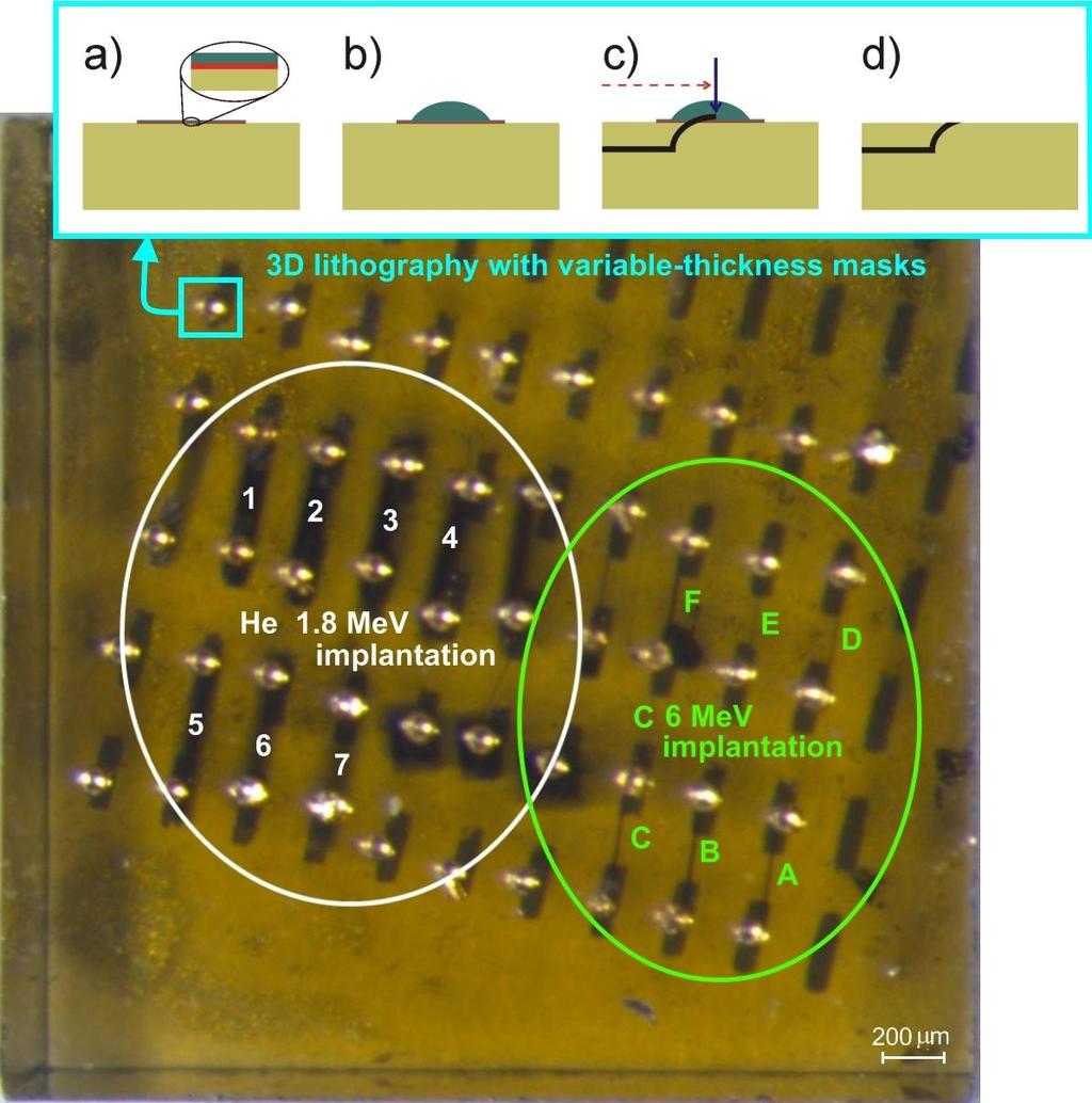
4 Experimental The process of damage induced by MeV ions in matter occurs mainly at the end of ion range, where the cross section for nuclear collisions is strongly enhanced, after the ion energy is progressively reduced by electronic interactions occurring in the initial stages of the ion path [19]. In Fig. 1 we report the damage density profiles of 6 MeV C and 1.8 MeV He ions as resulting from the Monte Carlo simulation with SRIM code [20]. The curves were calculated by setting a value of 50 ev for the atom displacement energy in the diamond lattice [21, 22]. As visible in Fig. 1, the high damage density at the end of range of the ions determines the formation of narrow damaged layers at depths of ~2.7 below the sample surface for 6 MeV C and 1.8 MeV He, respectively. The damage density induced by carbon ions is significantly higher with respect to helium ions, with an integrated number of vacancies per ion of 299 compared to 49, respectively. In order to electrically connect the endpoints of the channels to the surface contacts, a three-dimensional masking technique was employed to modulate the penetration depth of the ions from their range in the unmasked material up to the sample surface with increasing thickness of stopping material. The basic concept is shown schematically in the inset of Fig. 2, while further details can be found in [17]. The samples consist of synthetic single crystal diamonds classified as type Ib, with a substitutional nitrogen concentration comprised between 10 and 100 ppm. The diamonds were produced with high pressure high temperature (HPHT) synthesis by Sumitomo, and their size is mm. The samples are cut along the 100 crystal direction and they
5 are optically polished on the two opposite large faces. After the masking process, the samples were implanted at room temperature with two different ion species, namely carbon and helium. The implantation of 1.8 MeV He ions was performed at the microbeam line on the AN2000 accelerator facility of the INFN Legnaro National Laboratories (INFN-LNL). 6 MeV C ions were implanted at the microbeam line of the Laboratory for Ion Beam (LIBI-RBI). In both the implantations the ion beam was focused to a micrometric spot, and the ion current was ~0.8 na and ~0.3 5 na for the C ion and He ion respectively. The emission of backscattered ions or characteristic x-rays from the metal electrodes was employed to monitor the implantation fluence in real time respectively during C and He implantation, after a suitable calibration with a Faraday Cup. The accuracy of the fluence evaluation is estimated of the order of 20%, whereas the uncertainty is negligible. Before ion implantation, the sample was masked with semi-spherical contacts by means of a standard gold wire ball bonder commonly used for the contacting of microchip devices. In order to improve the adhesion of the gold contacts, Cr-Au adhesion areas were evaporated on the sample surface through a mask, as shown schematically in the inset of Fig. 2. The Cr and Au adhesion layers are <100 nm in thickness, therefore they do not affect significantly the depth at which the damaged layer is formed in diamond; on the other hand, the maximum thickness of the gold contacts is of the order of in their central regions, which is more than enough to fully stop the incident ions. Fig. 2 shows an optical image in transmission of a sample implanted with 1.8 MeV He and 6 MeV C at increasing fluences, in the ranges ( cm -2 ) and (
6 cm -2 ), respectively. The optically opaque implanted channels are clearly visible, together with the Cr/Au adhesion layers and the semi-spherical contacts. The electrical characterization was performed with a Semiconductor Parameter Analyzer (4145B Hewlett Packard) connected to a probe station (Alessi REL-4500). The IV curves were measured by positioning the two probe tips on the channels end-points and making a sweep in the ( V) range. Test IV measurements were performed between contacts that were connected through micro-channels, allowing an effective check that the measured conductivity is only relevant to the sub-superficial layers and not to spurious surface conductivity. Results and discussion Fig. 3 shows the measured IV curves; as expected, the IV characteristics are symmetrical with respect to the applied voltage polarity, therefore only the data in the V range are reported. Firstly, it is worth noticing that the IV curves systematically exhibit a higher conductivity for channels implanted at higher fluences with both He and C ions. The test measurement between unconnected contacts (not reported here) yield a current signal comparable with the instrumental noise ( A), therefore we can conclude that the conduction mechanism is entirely to be attributed to buried channels, with negligible contributions from surface conductivity. Secondly, a linear IV characteristic in the whole V range is observed only for channels implanted at low fluence, both for He and C implantations (see Fig. 3a), while a super-linear trend is systematically observed from channels implanted at higher fluences (see Fig. 3b).
7 In order to determine the transport mechanism at low electric fields as function of different irradiation conditions, a suitable scaling procedure of the electrical resistance of the channels and of the implantation fluences has been adopted. Firstly, since implantations performed with different ion species and energies determine significantly different damage profiles in the material (as shown schematically in Fig. 1), the fluences were re-scaled by multiplying their values with factors I i, defined as: (1) where subscript index i refers to the ion energy end species, d is the penetration range of the ions in diamond, and p i (z) is the damage linear density, expressed as the number of created vacancies per unit of penetration depth per incoming ion, i.e. the quantity plotted in Fig. 1. Therefore, since I i can be regarded as the total number of vacancies generated by a single ion (i.e. 299 vacancies for 6 MeV C ion and 49 vacancies for 1.8 MeV He ion), the product m,i * m,i I i m,i is the fluence of the m th implantation for the i th ion species and energy) can be interpreted as the total number of vacancies generated in the implantation per surface unit. Such an interpretation is valid only under the assumption that the local density of vacancies at a given depth (z) in the material, i.e. m,i (z), is directly proportional to the number of implanted ions, hence: (2) The above-mentioned assumption is indeed rather simplicistic, since it does not take into account non-linear processes occurring in the damage process, such as self-annealing, ballistic annealing and defect interaction. Nonetheless, the variable i* can be regarded as
8 a first-order parameter to re-scale fluences relevant to implantation processes performed with different ion species and energies. Concerning the electrical observable, the resistance of the channels in the low-field regime was evaluated from a linear fit of the IV data in the 0 1 V range, where all curves exhibit a linear trend. Moreover, a similar scaling process can be applied to the value of the channel resistivity, which is defined as R w L t, where R is the channel resistance, and w, t and L are its width, thickness and length, respectively. Again, since the buried channel is defined in the depth direction by a strongly non-uniform damage profile (see Fig. 1), the sheet resistance can be defined as R t *. Remarkably, w w while the ] vs [ions cm -2 ] plots yield to inconsistent results when data relevant to different implantation processes are merged, the relevant ] vs *[vacancies cm -2 ] plots result in satisfactory consistency, as shown in Fig. 4. In the above-mentioned plot, the sheet resistance exhibits a monotonous decrease in the range at increasing values of damage surface density in the vacancies cm -2, with satisfactory compatibility between data relevant to different implantation processes. Such scaling process can be employed also for the comparison of the above mentioned non-linearity of the IV characteristics as a function of implantation fluence. The field-enhanced transport mechanism in channels implanted at high fluences can be modelled with the power-law dependence I V. In Fig. 3 the fitting functions are reported with continuous lines, showing satisfactory agreement with the experimental data, both in the linear and super-linear regimes. Similarly to what reported above, the vs -2 ] plots yield to inconsistent results between the two implantation
9 processes, while the scaled *[vacancies cm -2 ] plot consistently shows a progressive increase of the parameter as a function of increasing damage density, from 1 (corresponding to linear behavior) up to Results of previous [18] conductance measurements in the temperature range K carried out on a single channel are compatible to the systematic data reported here, as shown in Fig.5. Moreover, they suggest that such super-linear behavior at moderate electric field (> 500 V cm -1 ) is to be ascribed to a space charge limited transport mechanism influenced by the trap type and distribution in the bandgap [23]. The behavior of as function of the damage density as shown in Fig. 3 seems to suggest the existence of a critical damage threshold occurring between and vacancies cm -2, and relevant to a transition from ohmic to space charge limited current transport mechanism in the moderate electric field region. Conclusions We reported about the fabrication and electrical characterization of buried conductive micro-channels in single crystal diamond with MeV ion induced damage. The analysis of the IV characteristics yielded significant parameters describing the conduction properties of the channels, namely the sheet resistance and the characteristic exponent ( ) of the power-law IV trend, which were expressed as a function of damage density. Satisfactory compatibility between the results obtained in different implantation conditions (ion species and energy) was achieved by suitably scaling the implantation fluences with parameters relevant to the different damage profiles. A peculiar evolution of the exponent as a function of the implantation fluence was identified, which will be investigated in further details in future works.
10 Acknowledgments
11 Figure captions Fig. 1: damage density profiles of 6 MeV C (dashed red line) and 1.8 MeV He (continuous blue line), expressed in linear density of generated vacancies per incoming ion, as resulting from the Monte Carlo simulation with SRIM code [20]; the high damage density at the end of ion range is clearly visible. Fig. 2: optical microscopy image in transmission of the implanted sample; the opaque micro- - - respectively) are clearly visible, together with the adhesion layers and the semi-spherical gold contacts. In the inset a cross-sectional schematic of the three-dimensional masking process is drawn; more details can be found in [17]. Fig. 3: IV curves of channels implanted with 1.8 MeV He and 6 MeV C ions at (a) low and (b) high fluences; while in the former case the IV curves are linear, in the latter case the curves follow a super-linear power-law dependence; experimental data are reported in dots, while fitting curves are reported in continuous lines. Fig. 4: log-log plot of the sheet resistance of the channels as a function of the damage surface density, for 1.8 MeV He (red dots) and 6 MeV C ions (black squares); the monotonous decrease exhibits a pseudo-exponential behavior.
12 Fig. 5: characteristic exponent of the power-law trend of the IV curve I V, as a function of the damage surface density, for 1.8 MeV He (red dots) and 6 MeV C ions (black squares); the monotonous increase exhibits a significant transition in the vacancies cm -2 range; the data are compatible with what reported in Ref. [18] for the IV characterization in temperature of a single channel (green dot).
13 References [1] V. S. Vavilov, V. V. Krasnopevtsev, Y. V. Milijutin, A. E. Gorodetsky, A. P. Zakharov, Radiat. Eff. 22 (1974) 141. [2] J. J. Hauser, J. R. Patel, Solid State Commun. 18 (1976) 789. [3] J. J. Hauser, J. R. Patel, J. W. Rodgers, Appl. Phys. Lett. 30 (1977) 129. [4] J. F. Prins, Radiat. Eff. Lett. 76 (1983) 79. [5] J. F. Prins, Phys. Rev. B 31 (1985) [6] S. Sato, M. Iwaki, Nucl. Instr. and Meth. B 32 (1988) 145. [7] S. Sato, H. Watanabe, K. Takahashi, Y. Abe, M. Iwaki, Nucl. Instr. and Meth. B 59 (1991) [8] S. Prawer, A. Hoffman, R. Kalish, Appl. Phys. Lett. 57 (1990) [9] S. Prawer, Diamond Relat. Mater. 4 (1995) 862. [10] S. Prawer, R. Kalish, Phys. Rev. B 51 (1995) [11] F. Fontaine, E. Gheeraert, A. Deneuville, Diamond Relat. Mater. 5 (1995) 572. [12] A. Reznik, V. Richter, R. Kalish, Phys. Rev. B 56 (1997) [13] A. Reznik, V. Richter, R. Kalish, Diamond Relat. Mater. 7 (1998) 317. [14] E. Baskin, A. Reznik, D. Saada, J. Adler, R. Kalish, Phys. Rev. B 64 (2001) [15] E. Trajkov, S. Prawer, Diamond Relat. Mater. 15 (2006) [16] A.A. Gippius, R.A. Khmelnitskiy, V.A. Dravin, S.D. Tkachenko, Diamond Relat. Mater. 8 (1999) 1631.
14 [17] P. Olivero, G. Amato, F. Bellotti, O. Budnyk, E. Colombo, M., C. Manfredotti, Z., F. Picollo, N. Skukan, M. Vannoni, E. Vittone, Diamond Relat. Mater. 18 (2009) [18] P. Olivero, G. Amato, F. Bellotti, S. Borini, A. Lo Giudice, F. Picollo, E. Vittone, European Physical Journal B, submitted (2009) [19] M. B. H. Breese, D. N. Jamieson, P. J. C. King, Material Analysis Using a Nuclear Microprobe, John Wiley and Sons Inc., New York, [20] J.F. Ziegler, The Stopping and Range of Ions in Solids, Pergamon, IIT, [21] W. Wu, S. Fahy, Phys. Rev., B 49 (1994) [22] D. Saada, J. Adler, R. Kalish, Int. J. Mod. Phys., C 9 (1998) 61. [23] A. Bozhko, M. Shupegin, T. Takagi, Diamond and Related Materials 11 (2002)
15
16
17
18
19
Keywords Diamond single crystal, Amorphous carbon, Ion implantation, Conduction mechanisms
 Direct fabrication and IV characterization of buried graphitic channels in diamond with MeV ion implantation P. Olivero 1, G. Amato 2, F. Bellotti 2, S. Borini 2, A. Lo Giudice 1, F. Picollo 1, E. Vittone
Controlled variation of the refractive index in ion-damaged diamond. of Excellence, University of Torino, via P. Giuria 1, Torino, Italy
 Controlled variation of the refractive index in ion-damaged diamond P. Olivero 1,2, S. Calusi 2,3, L. Giuntini 3, S. Lagomarsino 4, A. Lo Giudice 1,2, M. Massi 3, S. Sciortino 4, M. Vannoni 5, E. Vittone
A new protocol to evaluate the charge collection efficiency degradation in semiconductor devices induced by MeV ions
 Session 12: Modification and Damage: Contribute lecture O-35 A new protocol to evaluate the charge collection efficiency degradation in semiconductor devices induced by MeV ions Ettore Vittone Physics
Modeling of charge collection efficiency degradation in semiconductor devices induced by MeV ion beam irradiation
 Modeling of charge collection efficiency degradation in semiconductor devices induced by MeV ion beam irradiation Ettore Vittone Physics Department University of Torino - Italy 1 IAEA Coordinate Research
Ion Implantation ECE723
 Ion Implantation Topic covered: Process and Advantages of Ion Implantation Ion Distribution and Removal of Lattice Damage Simulation of Ion Implantation Range of Implanted Ions Ion Implantation is the
Implantation Energy Dependence on Deuterium Retention Behaviors for the Carbon Implanted Tungsten
 J. Plasma Fusion Res. SERIES, Vol. 10 (2013) Implantation Energy Dependence on Deuterium Retention Behaviors for the Carbon Implanted Tungsten Yasuhisa Oya 1) *, Makoto Kobayashi 1), Naoaki Yoshida 2),
Theory and practice of Materials Analysis for Microelectronics with a nuclear microprobe
 TUTORIAL Theory and practice of Materials Analysis for Microelectronics with a nuclear microprobe Ettore Vittone Physics Department University of Torino, Italy Ettore Vittone 1 IBIC for the functional
Pixels GaAs Detectors for Digital Radiography. M.E. Fantacci. and. Abstract
 Pixels GaAs Detectors for Digital Radiography M.E. Fantacci Dipartimento di Fisica dell'universita and Sezione I.N.F.N., Pisa, Italy and European Laboratory for Particle Physics (CERN), Geneve, Switzerland
Method of active correlations in the experiment 249 Cf+ 48 Ca n
 Method of active correlations in the experiment 249 Cf+ 48 Ca 297 118 +3n Yu.S.Tsyganov, A.M.Sukhov, A.N.Polyakov Abstract Two decay chains originated from the even-even isotope 294 118 produced in the
Ion Implant Part 1. Saroj Kumar Patra, TFE4180 Semiconductor Manufacturing Technology. Norwegian University of Science and Technology ( NTNU )
") 1 Ion Implant Part 1 Chapter 17: Semiconductor Manufacturing Technology by M. Quirk & J. Serda Spring Semester 2014 Saroj Kumar Patra,, Norwegian University of Science and Technology ( NTNU ) 2 Objectives
1 Ion Implant Part 1 Chapter 17: Semiconductor Manufacturing Technology by M. Quirk & J. Serda Spring Semester 2014 Saroj Kumar Patra,, Norwegian University of Science and Technology ( NTNU ) 2 Objectives
ABNORMAL X-RAY EMISSION FROM INSULATORS BOMBARDED WITH LOW ENERGY IONS
 302 ABNORMAL X-RAY EMISSION FROM INSULATORS BOMBARDED WITH LOW ENERGY IONS M. Song 1, K. Mitsuishi 1, M. Takeguchi 1, K. Furuya 1, R. C. Birtcher 2 1 High Voltage Electron Microscopy Station, National
Interaction of ion beams with matter
 Interaction of ion beams with matter Introduction Nuclear and electronic energy loss Radiation damage process Displacements by nuclear stopping Defects by electronic energy loss Defect-free irradiation
LOW-TEMPERATURE Si (111) HOMOEPITAXY AND DOPING MEDIATED BY A MONOLAYER OF Pb
 HOMOEPITAXY AND DOPING MEDIATED BY A MONOLAYER OF Pb") LOW-TEMPERATURE Si (111) HOMOEPITAXY AND DOPING MEDIATED BY A MONOLAYER OF Pb O.D. DUBON, P.G. EVANS, J.F. CHERVINSKY, F. SPAEPEN, M.J. AZIZ, and J.A. GOLOVCHENKO Division of Engineering and Applied Sciences,
LOW-TEMPERATURE Si (111) HOMOEPITAXY AND DOPING MEDIATED BY A MONOLAYER OF Pb O.D. DUBON, P.G. EVANS, J.F. CHERVINSKY, F. SPAEPEN, M.J. AZIZ, and J.A. GOLOVCHENKO Division of Engineering and Applied Sciences,
The scanning microbeam PIXE analysis facility at NIRS
 Nuclear Instruments and Methods in Physics Research B 210 (2003) 42 47 www.elsevier.com/locate/nimb The scanning microbeam PIXE analysis facility at NIRS Hitoshi Imaseki a, *, Masae Yukawa a, Frank Watt
GaN for use in harsh radiation environments
 4 th RD50 - Workshop on radiation hard semiconductor devices for very high luminosity colliders GaN for use in harsh radiation environments a (W Cunningham a, J Grant a, M Rahman a, E Gaubas b, J Vaitkus
Au-Ti THIN FILMS DEPOSITED ON GaAs
 Au-Ti THIN FILMS DEPOSITED ON GaAs R. V. GHITA *, D. PANTELICA**, M. F. LAZARESCU *, A. S. MANEA *, C. LOGOFATU *, C. NEGRILA *, V. CIUPINA *** * National Institute of Material Physics, P.O. Box MG7, Mãgurele,
Ion Implantation. alternative to diffusion for the introduction of dopants essentially a physical process, rather than chemical advantages:
 Ion Implantation alternative to diffusion for the introduction of dopants essentially a physical process, rather than chemical advantages: mass separation allows wide varies of dopants dose control: diffusion
DEVELOPMENT OF A NEW POSITRON LIFETIME SPECTROSCOPY TECHNIQUE FOR DEFECT CHARACTERIZATION IN THICK MATERIALS
 Copyright JCPDS - International Centre for Diffraction Data 2004, Advances in X-ray Analysis, Volume 47. 59 DEVELOPMENT OF A NEW POSITRON LIFETIME SPECTROSCOPY TECHNIQUE FOR DEFECT CHARACTERIZATION IN
physics/ Sep 1997
 GLAS-PPE/97-6 28 August 1997 Department of Physics & Astronomy Experimental Particle Physics Group Kelvin Building, University of Glasgow, Glasgow, G12 8QQ, Scotland. Telephone: +44 - ()141 3398855 Fax:
Highly charged ion beams applied to fabrication of Nano-scale 3D structures. Sadao MOMOTA Kochi University of Technology
 Highly charged ion beams applied to fabrication of Nano-scale 3D structures Sadao MOMOTA Kochi University of Technology Introduction 1 Prospect of microscopic structures 2D Semiconductor 3D Ex. MEMS http://www.rise.waseda.ac.jp/proj/sci/s98s08/j-s98s08.html
HIGH ENERGY IRRADIATION PROPERTIES OF CdTe/CdS SOLAR CELLS
 Presented at the 29 th PVSC, New Orleans (2002) HIGH ENERGY IRRADIATION PROPERTIES OF CdTe/CdS SOLAR CELLS D. L. Bätzner, A. Romeo, M. Döbeli 1, K. Weinert 2, H. Zogg, A. N. Tiwari Thin Film Physics Group,
Creation and annealing of point defects in germanium crystal lattices by subthreshold energy events
 Creation and annealing of point defects in germanium crystal lattices by subthreshold energy events University of Sevilla 203 Sergio M. M. Coelho, Juan F. R. Archilla 2 and F. Danie Auret Physics Department,
Semiconductor Detectors
 Semiconductor Detectors Summary of Last Lecture Band structure in Solids: Conduction band Conduction band thermal conductivity: E g > 5 ev Valence band Insulator Charge carrier in conductor: e - Charge
Joint ICTP-IAEA Workshop on Physics of Radiation Effect and its Simulation for Non-Metallic Condensed Matter.
 2359-3 Joint ICTP-IAEA Workshop on Physics of Radiation Effect and its Simulation for Non-Metallic Condensed Matter 13-24 August 2012 Electrically active defects in semiconductors induced by radiation
Chapter 4. Surface defects created by kev Xe ion irradiation on Ge
 81 Chapter 4 Surface defects created by kev Xe ion irradiation on Ge 4.1. Introduction As high energy ions penetrate into a solid, those ions can deposit kinetic energy in two processes: electronic excitation
Large electron screening effect in different environments
 Large electron screening effect in different environments Aleksandra Cvetinović, Matej Lipoglavsek, Sabina Markelj and Jelena Vesić Jožef Stefan Institute, Jamova cesta 39, Ljubljana, Slovenia Abstract
Implantation of labelled single nitrogen vacancy centers in diamond using 15 N
 Implantation of labelled single nitrogen vacancy centers in diamond using 15 N J. R. Rabeau *, P. Reichart School of Physics, Microanalytical Research Centre, The University of Melbourne, Parkville, Victoria
Comparisons of DFT-MD, TB- MD and classical MD calculations of radiation damage and plasmawallinteractions
 CMS Comparisons of DFT-MD, TB- MD and classical MD calculations of radiation damage and plasmawallinteractions Kai Nordlund Department of Physics and Helsinki Institute of Physics University of Helsinki,
Characterization of Irradiated Doping Profiles. Wolfgang Treberspurg, Thomas Bergauer, Marko Dragicevic, Manfred Krammer, Manfred Valentan
 Characterization of Irradiated Doping Profiles, Thomas Bergauer, Marko Dragicevic, Manfred Krammer, Manfred Valentan Vienna Conference on Instrumentation (VCI) 14.02.2013 14.02.2013 2 Content: Experimental
Focused-ion-beam milling based nanostencil mask fabrication for spin transfer torque studies. Güntherodt
 Focused-ion-beam milling based nanostencil mask fabrication for spin transfer torque studies B. Özyilmaz a, G. Richter, N. Müsgens, M. Fraune, M. Hawraneck, B. Beschoten b, and G. Güntherodt Physikalisches
Lab1. Resolution and Throughput of Ion Beam Lithography.
 1 ENS/PHY463 Lab1. Resolution and Throughput of Ion Beam Lithography. (SRIM 2008/2013 computer simulation) Objective The objective of this laboratory work is to evaluate the exposure depth, resolution,
Energetic particles and their detection in situ (particle detectors) Part II. George Gloeckler
 Part II. George Gloeckler") Energetic particles and their detection in situ (particle detectors) Part II George Gloeckler University of Michigan, Ann Arbor, MI University of Maryland, College Park, MD Simple particle detectors Gas-filled
Energetic particles and their detection in situ (particle detectors) Part II George Gloeckler University of Michigan, Ann Arbor, MI University of Maryland, College Park, MD Simple particle detectors Gas-filled
A new detector for neutron beam monitoring
 A new detector for neutron beam monitoring European Organization for Nuclear Research (CERN), Geneva, Switzerland in collaboration with Commissariat à l Energie Atomique (CEA), Saclay, France, Instituto
Fast Monte-Carlo Simulation of Ion Implantation. Binary Collision Approximation Implementation within ATHENA
 Fast Monte-Carlo Simulation of Ion Implantation Binary Collision Approximation Implementation within ATHENA Contents Simulation Challenges for Future Technologies Monte-Carlo Concepts and Models Atomic
Secondary ion mass spectrometry (SIMS)
") Secondary ion mass spectrometry (SIMS) ELEC-L3211 Postgraduate Course in Micro and Nanosciences Department of Micro and Nanosciences Personal motivation and experience on SIMS Offers the possibility to
Secondary ion mass spectrometry (SIMS) ELEC-L3211 Postgraduate Course in Micro and Nanosciences Department of Micro and Nanosciences Personal motivation and experience on SIMS Offers the possibility to
Supplementary Figure S1. AFM images of GraNRs grown with standard growth process. Each of these pictures show GraNRs prepared independently,
 Supplementary Figure S1. AFM images of GraNRs grown with standard growth process. Each of these pictures show GraNRs prepared independently, suggesting that the results is reproducible. Supplementary Figure
Secondary Ion Mass Spectrometry (SIMS) Thomas Sky
 Thomas Sky") 1 Secondary Ion Mass Spectrometry (SIMS) Thomas Sky Depth (µm) 2 Characterization of solar cells 0,0 1E16 1E17 1E18 1E19 1E20 0,2 0,4 0,6 0,8 1,0 1,2 P Concentration (cm -3 ) Characterization Optimization
1 Secondary Ion Mass Spectrometry (SIMS) Thomas Sky Depth (µm) 2 Characterization of solar cells 0,0 1E16 1E17 1E18 1E19 1E20 0,2 0,4 0,6 0,8 1,0 1,2 P Concentration (cm -3 ) Characterization Optimization
Bandgap engineering through nanocrystalline magnetic alloy grafting on. graphene
 Electronic Supplementary Material (ESI) for Physical Chemistry Chemical Physics. This journal is the Owner Societies 2014 Electronic Supplementary Information (ESI) for Bandgap engineering through nanocrystalline
Sputtering by Particle Bombardment
 Rainer Behrisch, Wolfgang Eckstein (Eds.) Sputtering by Particle Bombardment Experiments and Computer Calculations from Threshold to MeV Energies With 201 Figures e1 Springer Contents Introduction and
A Project for High Fluence 14 MeV Neutron Source
 A Project for High Fluence 14 MeV Neutron Source Mario Pillon 1, Maurizio Angelone 1, Aldo Pizzuto 1, Antonino Pietropaolo 1 1 Associazione ENEA-EURATOM Sulla Fusione, ENEA C.R. Frascati, via E. Fermi,
ABSTRACT 1. INTRODUCTION 2. EXPERIMENT
 Fabrication of Nanostructured Heterojunction LEDs Using Self-Forming Moth-Eye Type Arrays of n-zno Nanocones Grown on p-si (111) Substrates by Pulsed Laser Deposition D. J. Rogers 1, V. E. Sandana 1,2,3,
Electronic transport in low dimensional systems
 Electronic transport in low dimensional systems For example: 2D system l
International Journal of Scientific & Engineering Research, Volume 5, Issue 3, March-2014 ISSN
 316 Effective atomic number of composite materials by Compton scattering - nondestructive evaluation method Kiran K U a, Ravindraswami K b, Eshwarappa K M a and Somashekarappa H M c* a Government Science
, MgAl 2. and MgO irradiated with high energy heavy ions O 3
 Surface defects in Al 2, MgAl 2 O 4 and MgO irradiated with high energy heavy ions V.A.Skuratov 1, S.J. Zinkle 2 A.E.Efimov 1, K.Havancsak 3 1 Flerov Laboratory of Nuclear Reactions, JINR, Dubna, Russia
CLUSTER SIZE DEPENDENCE OF SPUTTERING YIELD BY CLUSTER ION BEAM IRRADIATION
 CLUSTER SIZE DEPENDENCE OF SPUTTERING YIELD BY CLUSTER ION BEAM IRRADIATION T. Seki 1,2), T. Murase 1), J. Matsuo 1) 1) Quantum Science and Engineering Center, Kyoto University 2) Collaborative Research
SUPPLEMENTARY INFORMATION
 doi:10.1038/nature11231 Materials and Methods: Sample fabrication: Highly oriented VO 2 thin films on Al 2 O 3 (0001) substrates were deposited by reactive sputtering from a vanadium target through reactive
Micro-patterned porous silicon using proton beam writing
 Micro-patterned porous silicon using proton beam writing M. B. H. Breese, D. Mangaiyarkarasi, E. J. Teo*, A. A. Bettiol and D. Blackwood* Centre for Ion Beam Applications, Department of Physics, National
Chapter 4 Scintillation Detectors
 Med Phys 4RA3, 4RB3/6R03 Radioisotopes and Radiation Methodology 4-1 4.1. Basic principle of the scintillator Chapter 4 Scintillation Detectors Scintillator Light sensor Ionizing radiation Light (visible,
M R S Internet Journal of Nitride Semiconductor Research
 Page 1 of 6 M R S Internet Journal of Nitride Semiconductor Research Volume 9, Article 7 The Ambient Temperature Effect on Current-Voltage Characteristics of Surface-Passivated GaN-Based Field-Effect Transistors
VLSI Technology Dr. Nandita Dasgupta Department of Electrical Engineering Indian Institute of Technology, Madras
 VLSI Technology Dr. Nandita Dasgupta Department of Electrical Engineering Indian Institute of Technology, Madras Lecture - 20 Ion-implantation systems and damages during implantation So, in our discussion
Soft Breakdown in Ultra-Thin Gate Oxides
 Soft Breakdown in Ultra-Thin Gate Oxides Dipartimento di Elettronica e Informatica Università di Padova via Gradenigo 6a, 35131 Padova, Italy Outline Introduction: radiation effects on thin oxide Radiation
Fission Enhanced diffusion of uranium in zirconia
 Fission Enhanced diffusion of uranium in zirconia N. Bérerd, A. Chevarier, N. Moncoffre, Institut de Physique Nucléaire de Lyon, 4, rue Enrico Fermi, 69622 Villeurbanne Cedex, France, Ph. Sainsot, Institut
arxiv: v1 [astro-ph] 30 Jul 2008
![arxiv: v1 [astro-ph] 30 Jul 2008](/thumbs/73/69036858.jpg "arxiv: v1 [astro-ph] 30 Jul 2008") arxiv:0807.4824v1 [astro-ph] 30 Jul 2008 THE AIR-FLUORESCENCE YIELD F. Arqueros, F. Blanco, D. Garcia-Pinto, M. Ortiz and J. Rosado Departmento de Fisica Atomica, Molecular y Nuclear, Facultad de Ciencias
arxiv:0807.4824v1 [astro-ph] 30 Jul 2008 THE AIR-FLUORESCENCE YIELD F. Arqueros, F. Blanco, D. Garcia-Pinto, M. Ortiz and J. Rosado Departmento de Fisica Atomica, Molecular y Nuclear, Facultad de Ciencias
SUPPLEMENTARY NOTES Supplementary Note 1: Fabrication of Scanning Thermal Microscopy Probes
 SUPPLEMENTARY NOTES Supplementary Note 1: Fabrication of Scanning Thermal Microscopy Probes Fabrication of the scanning thermal microscopy (SThM) probes is summarized in Supplementary Fig. 1 and proceeds
Supporting Information. Fast Synthesis of High-Performance Graphene by Rapid Thermal Chemical Vapor Deposition
 1 Supporting Information Fast Synthesis of High-Performance Graphene by Rapid Thermal Chemical Vapor Deposition Jaechul Ryu, 1,2, Youngsoo Kim, 4, Dongkwan Won, 1 Nayoung Kim, 1 Jin Sung Park, 1 Eun-Kyu
Lecture 7: Extrinsic semiconductors - Fermi level
 Lecture 7: Extrinsic semiconductors - Fermi level Contents 1 Dopant materials 1 2 E F in extrinsic semiconductors 5 3 Temperature dependence of carrier concentration 6 3.1 Low temperature regime (T < T
Radiation damage I. Steve Fitzgerald.
 Radiation damage I Steve Fitzgerald http://defects.materials.ox.ac.uk/ Firstly an apology Radiation damage is a vast area of research I cannot hope to cover much in any detail I will try and introduce
EE 212 FALL ION IMPLANTATION - Chapter 8 Basic Concepts
 EE 212 FALL 1999-00 ION IMPLANTATION - Chapter 8 Basic Concepts Ion implantation is the dominant method of doping used today. In spite of creating enormous lattice damage it is favored because: Large range
Energy Spectroscopy. Ex.: Fe/MgO
 Energy Spectroscopy Spectroscopy gives access to the electronic properties (and thus chemistry, magnetism,..) of the investigated system with thickness dependence Ex.: Fe/MgO Fe O Mg Control of the oxidation
Silver Thin Film Characterization
 Silver Thin Film Characterization.1 Introduction Thin films of Ag layered structures, typically less than a micron in thickness, are tailored to achieve desired functional properties. Typical characterization
Supporting Information. by Hexagonal Boron Nitride
 Supporting Information High Velocity Saturation in Graphene Encapsulated by Hexagonal Boron Nitride Megan A. Yamoah 1,2,, Wenmin Yang 1,3, Eric Pop 4,5,6, David Goldhaber-Gordon 1 * 1 Department of Physics,
Electrically active defects in semiconductors induced by radiation
 Electrically active defects in semiconductors induced by radiation Ivana Capan Rudjer Boskovic Institute, Croatia http://www.irb.hr/users/capan Outline Radiation damage Capacitance transient techniques
Energy fluxes in plasmas for fabrication of nanostructured materials
 Energy fluxes in plasmas for fabrication of nanostructured materials IEAP, Universität Kiel 2nd Graduate Summer Institute "Complex Plasmas" August 5-13, 2010 in Greifswald (Germany) AG 1 Outline Motivation
Comparison of the Wehner Spots With Angle Distribution Sputtered Atoms Materials
 Comparison of the Wehner Spots With Angle Distribution Sputtered Atoms Materials Dj. Boubetra and L.Selmani LMSE, Centre Universitaire de Bordj Bou Arreridj El Anasser 34265, Algeria boubetra@gmail.com
Imaging Methods: Scanning Force Microscopy (SFM / AFM)
") Imaging Methods: Scanning Force Microscopy (SFM / AFM) The atomic force microscope (AFM) probes the surface of a sample with a sharp tip, a couple of microns long and often less than 100 Å in diameter.
Imaging Methods: Scanning Force Microscopy (SFM / AFM) The atomic force microscope (AFM) probes the surface of a sample with a sharp tip, a couple of microns long and often less than 100 Å in diameter.
Stopping power for MeV 12 C ions in solids
 Nuclear Instruments and Methods in Physics Research B 35 (998) 69±74 Stopping power for MeV C ions in solids Zheng Tao, Lu Xiting *, Zhai Yongjun, Xia Zonghuang, Shen Dingyu, Wang Xuemei, Zhao Qiang Department
Supplementary Information
 Supplementary Information Supplementary Figures Supplementary figure S1: Characterisation of the electron beam intensity profile. (a) A 3D plot of beam intensity (grey value) with position, (b) the beam
In situ TEM studies of helium bubble/platelet evolution in Si based materials
 In situ TEM studies of helium bubble/platelet evolution in Si based materials M. Vallet 1, M.F. Beaufort 1, J.F. Barbot 1, E. Oliviero 2 and S.E. Donnelly 3 1 Institut Pprime, CNRS-Université de Poitiers,
Analysis of Ion Implantation Profiles for Accurate Process/Device Simulation: Analysis Based on Quasi-Crystal Extended LSS Theory
 Analysis of Ion Implantation Profiles for Accurate Process/Device Simulation: Analysis Based on Quasi-Crystal xtended LSS Theory Kunihiro Suzuki (Manuscript received December 8, 9) Ion implantation profiles
Radiation damage calculation in PHITS
 Radiation Effects in Superconducting Magnet Materials (RESMM'12), 13 Feb. 15 Feb. 2012 Radiation damage calculation in PHITS Y. Iwamoto 1, K. Niita 2, T. Sawai 1, R.M. Ronningen 3, T. Baumann 3 1 JAEA,
The limits of volume reflection in bent crystals
 The limits of volume reflection in bent crystals V.M. Biryukov Institute for High Energy Physics, Protvino, 142281, Russia Abstract We show that theory predictions for volume reflection in bent crystals
AP5301/ Name the major parts of an optical microscope and state their functions.
 Review Problems on Optical Microscopy AP5301/8301-2015 1. Name the major parts of an optical microscope and state their functions. 2. Compare the focal lengths of two glass converging lenses, one with
Ion Implanter Cyclotron Apparatus System
 Ion Implanter Cyclotron Apparatus System A. Latuszyñski, K. Pyszniak, A. DroŸdziel, D. M¹czka Institute of Physics, Maria Curie-Sk³odowska University, Lublin, Poland Abstract In this paper the authors
SIMULATION OF LASER INDUCED NUCLEAR REACTIONS
 NUCLEAR PHYSICS SIMULATION OF LASER INDUCED NUCLEAR REACTIONS K. SPOHR 1, R. CHAPMAN 1, K. LEDINGHAM 2,3, P. MCKENNA 2,3 1 The Institute of Physical Research, University of Paisley, Paisley PA1 2BE, UK
ELECTRIC FIELD INFLUENCE ON EMISSION OF CHARACTERISTIC X-RAY FROM Al 2 O 3 TARGETS BOMBARDED BY SLOW Xe + IONS
 390 ELECTRIC FIELD INFLUENCE ON EMISSION OF CHARACTERISTIC X-RAY FROM Al 2 O 3 TARGETS BOMBARDED BY SLOW Xe + IONS J. C. Rao 1, 2 *, M. Song 2, K. Mitsuishi 2, M. Takeguchi 2, K. Furuya 2 1 Department
Improvement of depth resolution of VEPAS by a sputtering technique
 Martin Luther University Halle Improvement of depth resolution of VEPAS by a sputtering technique R. Krause Rehberg, M. John, R. Böttger, W. Anwand and A. Wagner Martin Luther University Halle & HZDR Dresden
S1. X-ray photoelectron spectroscopy (XPS) survey spectrum of
 survey spectrum of") Site-selective local fluorination of graphene induced by focused ion beam irradiation Hu Li 1, Lakshya Daukiya 2, Soumyajyoti Haldar 3, Andreas Lindblad 4, Biplab Sanyal 3, Olle Eriksson 3, Dominique Aubel
Site-selective local fluorination of graphene induced by focused ion beam irradiation Hu Li 1, Lakshya Daukiya 2, Soumyajyoti Haldar 3, Andreas Lindblad 4, Biplab Sanyal 3, Olle Eriksson 3, Dominique Aubel
(a) (b) Supplementary Figure 1. (a) (b) (a) Supplementary Figure 2. (a) (b) (c) (d) (e)
 (b) Supplementary Figure 1. (a) (b) (a) Supplementary Figure 2. (a) (b) (c) (d) (e)") (a) (b) Supplementary Figure 1. (a) An AFM image of the device after the formation of the contact electrodes and the top gate dielectric Al 2 O 3. (b) A line scan performed along the white dashed line
(a) (b) Supplementary Figure 1. (a) An AFM image of the device after the formation of the contact electrodes and the top gate dielectric Al 2 O 3. (b) A line scan performed along the white dashed line
Stability of Semiconductor Memory Characteristics in a Radiation Environment
 SCIENTIFIC PUBLICATIONS OF THE STATE UNIVERSITY OF NOVI PAZAR SER. A: APPL. MATH. INFORM. AND MECH. vol. 7, 1 (2014), 33-39. Stability of Semiconductor Memory Characteristics in a Radiation Environment
Introduction into Positron Annihilation
 Introduction into Positron Annihilation Introduction (How to get positrons? What is special about positron annihilation?) The methods of positron annihilation (positron lifetime, Doppler broadening, ACAR...)
Lab 1. Resolution and Throughput of Ion Beam Lithography
 1 ENS/PHY463 Lab 1. Resolution and Throughput of Ion Beam Lithography (SRIM 2008/2013 computer simulation) Objective The objective of this laboratory work is to evaluate the exposure depth, resolution,
Universal valence-band picture of. the ferromagnetic semiconductor GaMnAs
 Universal valence-band picture of the ferromagnetic semiconductor GaMnAs Shinobu Ohya *, Kenta Takata, and Masaaki Tanaka Department of Electrical Engineering and Information Systems, The University of
Boron-based semiconductor solids as thermal neutron detectors
 Boron-based semiconductor solids as thermal neutron detectors Douglas S. McGregor 1 and Stan M. Vernon 2 1 S.M.A.R.T. Laboratory, Department of Nuclear Engineering and Radiological Sciences, University
Ion Beam Induced Luminescence (IBIL) for scintillator analysis
 for scintillator analysis") Ion Beam Induced Luminescence (IBIL) for scintillator analysis Alberto Quaranta Università di Trento Dipartimento dei Materiali e delle Tecnologie Industriali (DIMTI) Laboratori Nazionali di Legnaro -
Ion Beam Induced Luminescence (IBIL) for scintillator analysis Alberto Quaranta Università di Trento Dipartimento dei Materiali e delle Tecnologie Industriali (DIMTI) Laboratori Nazionali di Legnaro -
Mara Bruzzi INFN and University of Florence, Italy and SCIPP, UC Santa Cruz, USA
 SCIPP 06/16 September 2006 Capacitance-Voltage analysis at different temperatures in heavily irradiated silicon detectors Mara Bruzzi INFN and University of Florence, Italy and SCIPP, UC Santa Cruz, USA
SURFACE PROCESSING WITH HIGH-ENERGY GAS CLUSTER ION BEAMS
 SURFACE PROCESSING WITH HIGH-ENERGY GAS CLUSTER ION BEAMS Toshio Seki and Jiro Matsuo, Quantum Science and Engineering Center, Kyoto University, Gokasyo, Uji, Kyoto 611-0011, Japan Abstract Gas cluster
Opportunities for Advanced Plasma and Materials Research in National Security
 Opportunities for Advanced Plasma and Materials Research in National Security Prof. J.P. Allain allain@purdue.edu School of Nuclear Engineering Purdue University Outline: Plasma and Materials Research
MSN551 LITHOGRAPHY II
 MSN551 Introduction to Micro and Nano Fabrication LITHOGRAPHY II E-Beam, Focused Ion Beam and Soft Lithography Why need electron beam lithography? Smaller features are required By electronics industry:
NITROGEN CONTAINING ULTRA THIN SiO 2 FILMS ON Si OBTAINED BY ION IMPLANTATION
 NITROGEN CONTAINING ULTRA THIN SiO 2 FILMS ON Si OBTAINED BY ION IMPLANTATION Sashka Petrova Alexandrova 1, Evgenia Petrova Valcheva 2, Rumen Georgiev Kobilarov 1 1 Department of Applied Physics, Technical
Electrical isolation of n-type and p-type InP layers by proton bombardment
 JOURNAL OF APPLIED PHYSICS VOLUME 89, NUMBER 10 15 MAY 2001 Electrical isolation of n-type and p-type InP layers by proton bombardment H. Boudinov, a) H. H. Tan, and C. Jagadish Department of Electronic
Photon Energy Dependence of Contrast in Photoelectron Emission Microscopy of Si Devices
 Photon Energy Dependence of Contrast in Photoelectron Emission Microscopy of Si Devices V. W. Ballarotto, K. Siegrist, R. J. Phaneuf, and E. D. Williams University of Maryland and Laboratory for Physical
Light Interaction with Small Structures
 Light Interaction with Small Structures Molecules Light scattering due to harmonically driven dipole oscillator Nanoparticles Insulators Rayleigh Scattering (blue sky) Semiconductors...Resonance absorption
Chapter 3 Properties of Nanostructures
 Chapter 3 Properties of Nanostructures In Chapter 2, the reduction of the extent of a solid in one or more dimensions was shown to lead to a dramatic alteration of the overall behavior of the solids. Generally,
Single ion implantation for nanoelectronics and the application to biological systems. Iwao Ohdomari Waseda University Tokyo, Japan
 Single ion implantation for nanoelectronics and the application to biological systems Iwao Ohdomari Waseda University Tokyo, Japan Contents 1.History of single ion implantation (SII) 2.Novel applications
Screens for low current beams
 Screens for low current beams P.Finocchiaro, L.Cosentino, A.Pappalardo INFN - Laboratori Nazionali del Sud Catania, Italy Status Workshop on 29-Apr-2010 on Scintillating - Preliminary Screen Applications
Optical Characterization of Self-Assembled Si/SiGe Nano-Structures
 Optical Characterization of Self-Assembled Si/SiGe Nano-Structures T. Fromherz, W. Mac, G. Bauer Institut für Festkörper- u. Halbleiterphysik, Johannes Kepler Universität Linz, Altenbergerstraße 69, A-
Low Energy Nuclear Fusion Reactions in Solids
 Kasagi, J., et al. Low Energy Nuclear Fusion Reactions in Solids. in 8th International Conference on Cold Fusion. 2000. Lerici (La Spezia), Italy: Italian Physical Society, Bologna, Italy. Low Energy Nuclear
Development of a Radiation Hard CMOS Monolithic Pixel Sensor
 Development of a Radiation Hard CMOS Monolithic Pixel Sensor M. Battaglia 1,2, D. Bisello 3, D. Contarato 2, P. Denes 2, D. Doering 2, P. Giubilato 2,3, T.S. Kim 2, Z. Lee 2, S. Mattiazzo 3, V. Radmilovic
Monte Carlo study of medium-energy electron penetration in aluminium and silver
 NUKLEONIKA 015;60():361366 doi: 10.1515/nuka-015-0035 ORIGINAL PAPER Monte Carlo study of medium-energy electron penetration in aluminium and silver Asuman Aydın, Ali Peker Abstract. Monte Carlo simulations
Implant isolation of AlGaAs multilayer DBR
 Nuclear Instruments and Methods in Physics Research B 218 (2004) 381 385 www.elsevier.com/locate/nimb Implant isolation of AlGaAs multilayer DBR A.V.P. Coelho a, *, H. Boudinov a, T. v. Lippen b, H.H.