Chapter 4. Surface defects created by kev Xe ion irradiation on Ge
|
|
|
- Coral Franklin
- 5 years ago
- Views:
Transcription
1 81 Chapter 4 Surface defects created by kev Xe ion irradiation on Ge 4.1. Introduction As high energy ions penetrate into a solid, those ions can deposit kinetic energy in two processes: electronic excitation and ionization, and nuclear collision. Kinetic energy transfer between penetrating ions and target atoms takes place through collective processes of nuclear collisions in a displacement. The cascade evolution consists of three stages. The first stage lasts ~ 0.3 ps, i.e., approximately the period of a lattice vibration: in this stage, which is called collision cascade, the penetrating ions and displaced atoms slow down until they no longer displace more lattice atoms. In the second stage lasting from ~ 0.3 ps to ~ 3 ps, the collision cascade evolves into a thermal spike where atoms are set into violent motion; the deposited energy is converted into heat, and the high temperature in a thermal spike causes local melting in the crystal interior [1-5]. In the last stage after ~ 3 ps, the melt zone rapidly cools at the rate on the order of o C/s and resolidifies, attaining ambient temperature after ~ 10 ps and leaving behind vacancy-rich core [6]; only in simple lattice structures like fcc or bcc metals the atoms can return to the original crystal structures during resolidification process, while in more complicated structures like ordered alloys, compound semiconductors or oxides a highly disordered nonequilibrium phase is frozen in [6].
2 82 In metals local meting causes volume expansion in a thermal spike, and therefore pressure builds up inside the melt zone. If this melt zone is formed close to the surface, the pressure buildup may not be contained, and bulk atoms can be pushed toward the surface by viscous flow [3-5] or microexplosion [4,5], resulting in surface craters [7-13]. However, molecular dynamics simulation of 5 kev Ge ion irradiation on Ge, which has a negative volume of melting, demonstrated depression of surface layers but no surface crater formation [4]; the density of solid Ge is 5.32 g/cm 3 at room temperature and the density of liquid Ge is 5.49 g/cm 3 at 937 o C, the melting temperature of Ge. Surface crater formation due to high energy heavy ion impact strongly depends on cascade energy and cascade energy density [7], and has been observed experimentally on Au(001) irradiated by kev Bi ions [7], on Au(001) bombarded by kev Xe ions [8], on Ge(001) irradiated by 20 kev Ga ions [9], and on Pt(111) irradiated by 5 kev Xe ions [10]. The yield of surface craters, which is the number of surface crater produced per incident ion, is typically on the order of 1 percent due to the fluctuations in energy deposition in individual collision cascades [7,8,10]. If the bulk nanocavities discussed in chapter 3 appear on the surface during ion irradiation, crater-like surface defects will be formed. Those bulk nanocavities can appear on the surface through migration of nanocavities toward the surface or exposure of nanocavities by ion etching removal of material above the nanocavities. Nanocavities can migrate in the crystal interior through surface diffusion, volume diffusion and vapor transport processes during thermal annealing [14,15].
3 83 In addition to being able to create surface craters, a displacement cascade can enhance the mobility of precipitates and nanocavities through the interaction of melt zones with precipitates and nanocavities [16-18]. Discrete He nanocavity motion was observed during 400 kev Ar ion irradiation on Au [16,17], where dense collision cascades form, whereas no migration of He nanocavities was observed during 200 kev Xe ion irradiation on Al, where dilute collision cascades form [17,18]. Donnelly et al. also observed disappearance of many He nanocavities in Au during 400 kev Ar ion irradiation and proposed that some nanocavities may appear on the surface while most nanocavities are likely to be disintegrated by displacement cascades [16,17]. In my experimental results, large surface defects, which resemble surface craters but will be called pits, are formed on the Ge surfaces irradiated by Xe ions with energies ranging from 650 ev to 20 kev at temperatures between 245 o C and 305 o C; the term pits used in this chapter implies surface defects more than one bilayer or monolayer deep and formed in a different manner than surface craters created by single ion displacement cascades. These pits appear only when the Ge starting surfaces are prepared by ion etching at T 400 o C and thus nanocavities are present in the bulk. Also the number of pits initially increases and then decreases with increasing ion fluence. These results suggest the pits are not surface craters and support the proposed formation mechanism of pits, which is sudden annihilation of bulk nanocavities on the surface through the interaction of a melt zone with a bulk nanocavity during kev Xe ion irradiation.
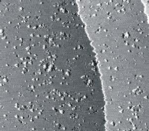
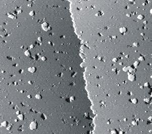
4 Results and discussion Formation of pits Fig. 4.1 shows STM images of the Ge surfaces following 5 kev Xe ion irradiation on the Ge starting surfaces displayed in Fig. 2.3 for 18 seconds with the ion fluence of ions/cm 2 ; this ion fluence corresponds to 1.2 bilayer removal for Ge(111) and 2.7 monolayers removal for Ge(001). Fig. 4.1(a) and (b) are Ge(111) surfaces irradiated at 275 o C and 305 o C respectively, and Fig. 4.1(c) and (d) are Ge(001) surfaces irradiated at 275 o C and 305 o C respectively. Large pits are formed on the Ge surfaces while no pits are observed on the Ge starting surfaces. Small area scans in Fig. 4.2 show the pits are surrounded by closely spaced steps. The size of the pits is larger at 305 o C than at 275 o C and on Ge(111) than on Ge(001); the average diameter of the pits in Fig. 4.1(a) is 24 nm and that in Fig. 4.1(b) is 40 nm, either of which is much larger than the diameter of the surface craters created by 20 kev Ga ions on Ge(001) at room temperature, ~ 6 nm [9]. Fig. 4.3 displays STM images of the Ge surfaces following 5 kev Xe ion irradiation for 3 minutes with the ion fluence of ions/cm 2 ; the ion fluence of ions/cm 2 corresponds to 12 bilayers removal for Ge(111) and 27 monolayers removal for Ge(001). Fig. 4.3(a) and (b) are Ge(111) surfaces etched at 275 o C and 305 o C respectively, and Fig. 4.3(c) is Ge(001) surface etched at 305 o C. Fig. 4.4 shows STM images of the Ge surfaces following 5 kev Xe ion irradiation for 30 minutes with the ion fluence of ions/cm 2 for Fig. 4.4(a), (c) and (d), and ions/cm 2 for Fig. 4.4(b); the ion fluence of ions/cm 2 corresponds to 120 bilayers removal for
5 85 Ge(111) and 270 monolayers removal for Ge(001), and the ion fluence of ions/cm 2 corresponds to 77 bilayers removal for Ge(111). Fig. 4.4(a) and (b) are Ge(111) surfaces etched at 275 o C and 305 o C respectively, and Fig. 4.4(c) and (d) are Ge(001) surfaces etched at 275 o C and 305 o C respectively. The number and size of the pits diminish both on Ge(111) and Ge(001) compared to Fig The number of pits is counted from STM images and plotted as a function of ion fluence for 650 ev, 5 kev and 20 kev Xe ion irradiation experiments in Fig. 4.5; for the experiments with Xe ion energy lower than 20 kev, Ge starting surfaces are prepared by 5 kev Xe ion etching at 520 o C for 30 minutes with the ion fluence of ions/cm 2, and for the 20 kev Xe ion irradiation experiments Ge starting surfaces are prepared by 5 kev Xe ion etching at 520 o C for 53 minutes with the ion fluence of ions/cm 2. The error bars are inserted assuming the statistics of the pits follows Poisson distribution where the error is the square root of the average. More pits are formed on Ge(001) than on Ge(111) both at 275 o C and 305 o C, and at 275 o C than at 305 o C both on Ge(001) and Ge(111). The pits completely disappear after 5 kev Xe ion irradiation with the ion fluence of ions/cm 2 on Ge(111). If the pits are surface craters, the number of pits should increase and the size of pits should grow with increasing ion fluence as observed in porous structure on Ge [9,19]. Therefore Fig. 4.4 and 4.5 suggest that pits are not surface craters, which are created by microexplosion or viscous flow through single ion displacement cascades.
6 86 Fig. 4.6 displays STM images of the Ge surfaces following 650 ev Xe ion irradiation on the starting surfaces displayed in Fig. 2.3 at 245 o C for 12 minutes 40 seconds with the ion fluence of ions/cm 2 ; this ion fluence corresponds to 1.2 bilayer removal for Ge(111) in Fig. 4.6(a) and 2.7 monolayers removal for Ge(001) in Fig. 4.6(b) [20], the same amount of material removed with the Ge surfaces shown in Fig Pits as large as those produced by 5 kev Xe ions are observed with lower density than Fig Surface crater formation strongly depends on cascade energy and cascade energy density [7], and thus a 650 ev Xe ion is improbable to create a 40 nm-diameter crater. Therefore, Fig. 4.6 also suggests that the pits are not surface craters. Fig. 4.7 shows annealing experiments of irradiated Ge(111) at 305 o C: Fig. 4.7(a) is the Ge(111) surface irradiated by 5 kev Xe ions at 305 o C for 5 seconds with the ion fluence of ions/cm 2, corresponding to removal of 0.33 bilayer or 0.11 nm thickness, Fig. 4.7(b) is the Ge(111) surface subsequently annealed for 30 minutes at 305 o C, and Fig. 4.7(c) is the Ge(111) surface irradiated by 5 kev Xe ions at 305 o C for 1 minute with the ion fluence of ions/cm 2, corresponding to removal of 3.9 bilayers or 1.3 nm thickness, Fig. 4.7(d) is the Ge(111) surface subsequently annealed for 30 minutes at 305 o C. Individual pits disappear with the annealing at 305 o C, while larger pits formed by coalescence of individual pits remain without much change in size after the annealing at 305 o C.
7 Formation mechanism of pits Diminishing number and size of pits with increasing ion fluence and formation of pits by 650 ev Xe ions suggest pits are not surface craters. 5 kev Xe ion irradiation at 275 o C on a Ge(111) buffer layer, which had been grown at 365 o C with the thickness of in an in situ MBE chamber, was performed to examine the interaction of 5 kev Xe ions with the starting surface prepared without ion etching at high temperature; this experiment revealed vacancy islands but no pits. Also annealing of the Ge(111) starting surface shown in Fig. 2.3(a) for 18 seconds at 305 o C was performed and neither pits nor vacancy islands were observed. The result that 650 ev Xe ions can create large pits suggests the formation of pits does not depend on ion energy as strongly as the formation of surface craters. The observation that the number of pits diminishes with the increasing ion fluence > ions/cm 2 implies the formation of pits depends on processes that diminish with ion irradiation. The fact that pits do not appear with 5 kev Xe ion irradiation on an MBE grown Ge(111) buffer layer suggests the formation of pits is associated with the bulk nanocavities discussed in chapter 3. As discussed in chapter 3, since there is a denuded zone for bulk nanocavities with the depth of ~ 4 nm from the surface where no nanocavities are observed, the formation of pits is not due to exposing bulk nanocavities by ion etching removal of material above the nanocavities considering the formation of pits after 0.11 nm thick Ge surface layer removal by 5 kev Xe ions in 4.7(a). In addition, the result that annealing of Ge(111) starting surface at 305 o C does not reveal pits
8 88 suggests the formation of pits is not mainly due to thermal migration of bulk nanocavities toward the surface. Therefore I propose that the pits are produced due to migration of bulk nanocavities toward the surface through the interaction of subsurface displacement cascades with bulk nanocavities; this interaction is responsible for the enhanced mobility of bulk nanocavities and thus for the formation of pits on the surface. Lacking the atomic level understanding of the interaction of a displacement cascade with a nanocavity, I propose that a collision cascade initiated adjacent to a nanocavity will form a melt zone that will allow the nanocavity to deform into the molten region, and if this melt zone intersects the surface, the nanocavity can be pulled out toward the surface during recrystallization process. Once appearing on the surface, pits become larger due to thermal diffusion of surface vacancies or adatoms, hence larger pits are formed at 305 o C than at 275 o C in Fig. 4.1 and individual pits eventually disappear with the annealing at 305 o C in Fig. 4.7(b) and (d). This proposed formation mechanism of pits can elucidate the existence of a denuded zone for bulk nanocavities, starting surfaces without pits, and behaviors of pits shown in Fig First, the denuded zone for bulk nanocavities with the depth of ~ 4 nm from the surface can be formed by 5 kev Xe ion etching at 520 o C since the nanocavities remaining in the zone will be annihilated on the surface due to the proposed interaction of displacement cascades with nanocavities. The depth of the denuded zone is approximately equal to the predicted 5 kev Xe ion penetration depth in Ge with ion incidence angle of 50 o from surface normal. Second, once those nanocavities appear on
9 89 the surface at 520 o C, pits flatten rapidly through surface diffusion of vacancies or adatoms to eventually disappear and therefore no pits are observed on the Ge starting surfaces. Third, with increasing ion fluence the number of pits initially increases as more bulk nanocavities appear on the surface, and eventually decreases as the bulk nanocavities are consumed. The number of pits formed on Ge(111) at 305 o C by 5 kev Xe ions shown in Fig. 4.5 and the areal density of nanocavities formed in the Ge(111) sample at 500 o C are plotted in Fig. 4.8; the areal density of nanocavities is calculated by integrating the average nanocavity density shown in Fig. 3.3 with base of 10 nm-thick depth. The similarity between the two plots also suggests that the pits are formed by annihilation of nanocavities. In addition, since higher energy ions can produce deeper displacement cascades, the result that 20 kev Xe ions produce more pits than 5 kev Xe ions by a factor of 4 with the ion fluence of ~ ions/cm 2 in Fig. 4.5 also suggests that the pits are formed by annihilation of nanocavities. The initial increase in the number of pits on Ge(001) is not linear with the ion fluence compared to the almost linearity on Ge(111) and more pits are observed on Ge(001) than on Ge(111) in Fig. 4.5; since the number of pits depends on the areal density of nanocavities, I believe there is a difference in the formation of bulk nanocavities in Ge(111) and Ge(001) probably due to the difference in the areal density of surface sites, which is proportional to sink strength of the surface, in the Eq. (1-21); Ge(001) with the surface site density of atoms/cm 2 is a weaker sink for vacancies compared to Ge(111) with the surface site density of atoms/cm 2. In
10 90 other words, only nanocavities large enough to absorb vacancies in competition with the surface can be nucleated and in the presence of stronger sink such as Ge(111) nanocavities larger than in Ge(001) can survive the competition; therefore, smaller number of larger pits results on Ge(111) than Ge(001) Individual impact of 20 kev Xe ions on Ge Fig. 4.9 shows STM images of the Ge(111) surfaces following 20 kev Xe ion irradiation at 275 o C; the ion fluence is ions/cm 2 corresponding to bilayer removal for 4.9(a), ions/cm 2 corresponding to 0.14 bilayer removal for 4.9(b), ions/cm 2 corresponding to 0.41 bilayer removal for 4.9(c) and ions/cm 2 corresponding to 1.9 bilayer removal for 4.9(d). Two types of prominent surface defects are observed: one is large pits formed by the annihilation of bulk nanocavities on the surface as discussed in section and the other is small pits. The difference in size between large and small pits is a factor of 2 in Fig. 4.9(a), and as ion irradiation continues the size difference between those two types of pits becomes more prominent. The small pits are more than one bilayer deep in comparison to one bilayer deep vacancy islands, and thus small pits are not formed by sputtering removal of surface atoms. Just like large pits, the number of small pits initially increases and then decreases with increasing ion fluence as shown in Fig. 4.10, and the number of small pits created at 215 o C is larger than at 275 o C. The initial increase in the number of small pits is not linear in Fig. 4.10, which can also be seen in Fig. 4.9(a) and (b); though the ion fluence is
11 91 9 times larger in Fig. 4.9(b) than in Fig. 4.9(a), the number of small pits is not proportionally larger. Also, in Fig. 4.9 and 4.10, the number of small pits decreases dramatically with the ion fluence of ~ ions/cm 2. I believe the small pits are annealed out much like the large pits in Fig. 4.7 with the resulting vacancies absorbed by the large pits or attached to the step edges or vacancy islands, and also recombine with the adatoms created along with the small pits during ion irradiation; hence the yield of the small pits in Fig is not constant. Fig displays STM images of the Ge(111) surfaces following 20 kev Xe ion irradiation with the ion fluence of ions/cm 2 corresponding to bilayer removal; the sample temperature during ion irradiation is 190 o C for 4.11(a), 215 o C for 4.11(b), and 245 o C for 4.11(c). Adatom islands are formed at 190 o C and 215 o C but not at 245 o C, and the number of small pits diminishes while the size of small pits grows as temperature increases from 215 o C to 245 o C. Small area scans reveal small pits and adatom islands more clearly as shown in Fig and the size of small pits grows as temperature increases from 190 o C to 215 o C. Also the density of adatom islands decreases while the size of adatom islands grows as temperature increases from 190 o C to 215 o C. Fig shows STM images of the Ge(111) surfaces following 20 kev Xe ion irradiation with the ion fluence of ions/cm 2 corresponding to 0.14 bilayer removal; the sample temperature during ion irradiation is 190 o C for 4.13(a), 215 o C for 4.13(b), 245 o C for 4.13(c), and 305 o C for 4.13(d). Comparing Fig. 4.13(a) and (b) with
12 92 Fig. 4.11(a) and (b), larger but less adatom islands are formed at 190 o C and 215 o C, and the size of small pits does not vary much, while the number of small pits is smaller in Fig. 4.13(c) than Fig. 4.11(c) though the ion fluence is increased by a factor 3. At 305 o C almost no small pits are observed. In addition, large pits are observed in Fig. 4.13(c) and (d) but not in Fig. 4.11(c). I propose that small pits and adatoms are produced via surface damage creation process by single 20 kev Xe ion impact on Ge(111) since I did not obtain experimental evidence that the small pits are surface craters as observed on Ge(001) bombarded by 20 kev Ga ions in Ref. 9. Besides, since the small pits are more than one bilayer deep, the small pits are not vacancy islands. 20 kev Xe ion irradiation on Ge(111) with the ion fluence of ions/cm 2 at room temperature revealed small pits, which are not surrounded by rims, whose size is ~ 1.5 nm compared to ~ 6 nm surface craters observed in Ref. 9; these small pits on the Ge(111) surface rather resembles small scale damage features in Ref. 9. In addition, the yield of small pits produced by 20 kev Xe ions on Ge(111) is ~ 0.5 %, which is a factor of 5 larger than the yield of surface craters in Ref. 9. Since 20 kev Xe ions can deposit the same amount of kinetic energy in a shallower depth than 20 kev Ga ions, if 20 kev Ga ions can create surface craters, 20 kev Xe ions can also create surface craters. However, the absence of surface craters on Ge(111) irradiated by 20 kev Xe ions and low yield of ~ 0.1 % for surface crater formation by 20 kev Ga ions on Ge(001) lead me to believe the possibility that during 20 kev Ga ion bombardment doubly or higher charged Ga ions or clustered Ga ions were formed in the ion beam with low but not negligible probability and those ions produced
13 93 surface craters. Threshold energy for Xe ions to create surface craters on Ge should be higher than 20 kev, although I do not yet know the exact threshold energy. Since the atomic mass of Ga is 70, 20 kev Ga + 2 ions would not have much different impact compared to 20 kev Xe + ions whose mass is 131. However, I believe 40 kev Ga 2+ 2 or higher charged clustered Ga ions accelerated by 20 kv would be able to create surface craters on Ge. For example, Merkle and Jäger observed that threshold energy for surface crater formation on Au decreases from 50 kev for Bi + ions to 12 kev for Bi + 2 ions due to increased deposited energy density for Bi + 2 ions [7]. The small pits created by surface damage creation can recombine with adatoms and disappear as temperature increases considering the absence of adatom islands on the Ge(111) surface and almost unchanged size of small pits in Fig. 4.11(c) and Fig. 4.13(c), and therefore less small pits are observed at 245 o C and 305 o C in Fig and Also as more adatoms are produced by ion irradiation, small pits are more likely to be filled with adatoms produced through the formation of nearby small pits. Fig shows an STM image of the Ge(111) surface annealed for 90 seconds at 275 o C after producing the surface shown in Fig. 4.13(b). Though large pits are not observed in Fig. 4.13(b), annealing the surface at 275 o C reveals large pits. As discussed in section 4.2.2, since thermal annealing alone cannot cause bulk nanocavities to migrate toward and appear on the surface, those large pits should be present in Fig. 4.13(b) but are not clearly distinguished from small pits. In agreement with the proposed mechanism of large pits formation discussed in section 4.2.2, this appearance of large pits is due to
14 94 thermal diffusion of surface vacancies or adatoms while small pits disappear during annealing.


 surface in (a) and")
 surface in (c) and")
15 95 (a) (b) (c) (d) Fig STM images of Ge irradiated by 5 kev Xe ions for 18 seconds on the starting surfaces shown in Fig. 2.3 with the ion flux of ions/cm 2 s, corresponding to 1.2 bilayer removal from the Ge(111) surface in (a) and (b), and 2.7 monolayers removal from the Ge(001) surface in (c) and (d). The scan size is nm 2. Temperature of samples during ion irradiation is: (a) 275 o C (b) 305 o C (c) 275 o C (d) 305 o C.

 and (b) Fig. 4.1(d).")
16 Fig High resolution STM images of Ge irradiated by 5 kev Xe ions at 305 o C corresponding to (a) Fig. 4.1(b) and (b) Fig. 4.1(d). The scan size is (a) nm 2 and (b) nm 2. 96


 surface in (c). The scan size is 600 600 nm 2.")
17 97 (a) (b) (c) Fig STM images of Ge irradiated by 5 kev Xe ions for 3 minutes on the starting surfaces shown in Fig. 2.3 with the ion flux of ions/cm 2 s, corresponding to 12 bilayers removal from the Ge(111) surface in (a) and (b), and 27 monolayers removal from the Ge(001) surface in (c). The scan size is nm 2. Temperature of samples during ion irradiation is: (a) 275 o C (b) 305 o C (c) 305 o C.


 surface in (a), 77 bilayers removal from the Ge(111)")
 and (d). The scan size is 600 600 nm 2.")
18 98 (a) (b) (c) (d) Fig STM images of Ge irradiated by 5 kev Xe ions for 30 minutes (in (a), (b) and (d)) and 20 minutes (in (b)) on the starting surfaces shown in Fig. 2.3 with the ion flux of ions/cm 2 s, corresponding to 120 bilayers removal from the Ge(111) surface in (a), 77 bilayers removal from the Ge(111) surface in (b), and 270 monolayers removal from the Ge(001) surface in (c) and (d). The scan size is nm 2. Temperature of samples during ion irradiation is: (a) 275 o C (b) 305 o C (c) 275 o C (d) 305 o C.
19 99 ion fluence (cm -2 ) kev 5 kev 650 ev thickness removed (nm) Fig The number of pits as a function of the ion fluence. Filled symbols are Ge samples irradiated by 5 kev Xe ions. Sample orientation and temperature are : (111), 305 o C; : (111), 275 o C; : (001), 305 o C; : (001), 275 o C. Open symbols are Ge(111) samples irradiated by 20 kev Xe ions. Sample temperature is : 275 o C, : 215 o C, : 245 o C and : 305 o C. and + are Ge(001) and Ge(111) samples irradiated by 650 ev Xe ions at 245 o C, respectively.


20 100 Fig STM images of Ge irradiated by 650 ev Xe ions at 245 o C for 12 minutes 40 seconds on the starting surfaces shown in Fig. 2.3 with the ion fluence of
21 ions/cm 2, corresponding to 1.2 bilayer removal from the Ge(111) surface in (a), and 2.7 monolayers removal from the Ge(001) surface in (b). The scan size is nm
 (a) irradiated by 5 kev Xe ions at 305 o")

 irradiated by 5 kev Xe ions at")

22 102 (a) (b) (c) (d) Fig STM images of Ge(111) (a) irradiated by 5 kev Xe ions at 305 o C for 5 seconds with the ion flux of ions/cm 2 s, corresponding to 0.33 bilayer removal from the surface (b) subsequently annealed for 30 minutes at 305 o C (c) irradiated by 5 kev Xe ions at 305 o C for 1 minute with the ion flux of ions/cm 2 s, corresponding to 3.9 bilayers removal from the surface (d) subsequently annealed for 30 minutes at 305 o C. The scan size is nm 2.
23 nanocavities formed in Ge(111) at 500 o C 10 pits formed on Ge(111) at 275 o C depth (nm) Fig The number of pits and nanocavities as a function of depth from the Ge surface. The number of pits is obtained from STM images as in Fig. 4.5 and the number of nanocavities is obtained from TEM images as in Fig The areal density of nanocavities is calculated by integrating the average nanocavity density shown in Fig. 3.4 with base of 10 nm-thick depth.
 irradiated by 20 kev Xe ions at 275")


24 104 (a) (b) (c) (d) Fig STM images of Ge(111) irradiated by 20 kev Xe ions at 275 o C with the ion fluence of (a) ions/cm 2, corresponding to bilayer removal from the surface (b) ions/cm 2, corresponding to 0.14 bilayer removal from the surface (c) ions/cm 2, corresponding to 0.41 bilayer removal from the surface (d) ions/cm 2, corresponding to 1.9 bilayer removal from the surface. The scan size is nm 2.
25 105 thickness removed (nm) o C o C ion fluence (cm -2 ) Fig The number of small pits as a function of the ion fluence. The error bars are inserted assuming the statistics of small pits follows Poisson distribution.
 irradiated by 20")

 190 o C (b) 215 o C (c) 245 o C.")
26 106 (a) (b) (c) Fig STM images of Ge(111) irradiated by 20 kev Xe ions with the ion fluence of ions/cm 2, corresponding to bilayer removal from the surface at (a) 190 o C (b) 215 o C (c) 245 o C. The scan size is nm 2.
27 107
28 108 Fig STM images of Ge(111) irradiated by 20 kev Xe ions with the ion fluence of ions/cm 2, corresponding to bilayer removal from the surface at (a) 190 o C (b) 215 o C. The scan size is nm 2.
 irradiated")


 245 o C (d) 305 o C.")
29 109 (a) (b) (c) (d) Fig STM images of Ge(111) irradiated by 20 kev Xe ions with the ion fluence of ions/cm 2, corresponding to 0.14 bilayer removal from the surface at (a) 190 o C (b) 215 o C (c) 245 o C (d) 305 o C. The scan size is nm 2.
 are observed. The scan size is 400 400 nm 2. 4.3. References")
30 110 Fig STM image of Ge(111) annealed for 90 seconds at 275 o C after obtaining the surface displayed in Fig. 4.13(b). Large pits which were not observed in Fig. 4.13(b) are observed. The scan size is nm References
31 111 [1] D. N. Seidman, R. S. Averback, and R. Benedek, Phys. Stat. Sol. 144, 85 (1987). [2] T. Diaz de la Rubia, R. S. Averback, R. Benedek, and W. E. King, Phys. Rev. Lett. 59, 1930 (1987). [3] R. S. Averback and Mai Ghaly, J. Appl. Phys. 76, 3908 (1994); Mai Ghaly and R. S. Averback, Phys. Rev. Lett. 72, 364 (1994). [4] Mai Ghaly, R. S. Averback, and T. Diaz de la Rubia, Nucl. Instr. Meth. Phys. Res. B 102, 51 (1995). [5] R. S. Averback, M. Ghaly and H. Zhu, in Film Synthesis and Growth Using Energetic Beams. Mat. Res. Soc. Symp. Proc. 388 (Materials Research Society, Pittsburgh, 1995) pp [6] P. Ehrhart, W. Schilling, and H. Ullmaier in Encyclopedia of Applied Physics, edited by George L. Trigg (VCH Publishers, New York, 1996). [7] K. L. Merkle and W. Jäger, Philos. Mag. A 44, 741 (1981). [8] S. E. Donnelly and R. C. Birtcher, Phys. Rev. B 56, (1997); R. C. Birtcher and S. E. Donnelly, Mat. Chem. Phys. 54, 111 (1998). [9] P. Bellon, S. Jay Chey, Joseph E. Van Nostrand, Mai Ghaly, David G. Cahill, and R. S. Averback, Surf. Sci. 339, 135 (1995). [10] Christian Teichert, Michael Hohage, Thomas Michely, and George Comsa, Phys. Rev. Lett. 72, 1682 (1994). [11] G. Foti, G. Vitali, and J. A. Davies, Rad. Effects 32, 187 (1977). [12] I. H. Wilson, N. J. Zheng, U. Knipping, and I. S. T. Tsong, Phys. Rev. B 38, 8444 (1988).
32 112 [13] I. H. Wilson, Y. J. Chen, J. B. Xu, R. A. B. Devine, and C. Jeynes, Surf. Int. Anal. 24, 881 (1996). [14] P. J. Goodhew and S. K. Tyler, Proc. R. Soc. Lond. A 377, 151 (1981). [15] H. Yamaguchi, I. Hashimoto, H. Mitsuya, K. Nakamura, E. Yagi, and M. Iwaki, J. Nucl. Mater. 161, 164 (1989). [16] S. E. Donnelly, R. C. Birtcher, C. Templier, and V. Vishnyakov, Phys. Rev. B 52, 3970 (1995) [17] S. E. Donnelly, R. C. Birtcher, C. Templier, R. Valizadeh, and V. Vishnyakov, Mat. Res. Soc. Symp. Proc. 373, 243 (1995). [18] R. C. Birtcher, S. E. Donnelly, and C. Templier, Phys. Rev. B 50, 764 (1994). [19] I. H. Wilson, J. Appl. Phys. 53, 1698 (1982). [20] A. L. Southern, William R. Willis, and Mark T. Robinson, J. Appl. Phys. 34, 153 (1963); G. S. Anderson, J. Appl. Phys. 37, 2838 (1966). The sputtering yield of 650 ev Ar ion is 1.3 on Ge(111) and Ge(001), which is approximately the sputtering yield of 650 ev Xe ion on Ge(111) and Ge(001).
Molecular Dynamics Study of Plasma Surface Interactions for Mixed Materials
 J. Plasma Fusion Res. SERIES, Vol. 9 () Molecular Dynamics Study of Plasma Surface Interactions for Mixed Materials Kaoru OHYA, Naohide MOHARA, Kensuke INAI, Atsushi ITO, Hiroaki NAKAMURA, Yoshio UEDA
Spontaneous Pattern Formation from Focused and Unfocused Ion Beam Irradiation
 Mat. Res. Soc. Symp. Proc. Vol. 696 2002 Materials Research Society Spontaneous Pattern Formation from Focused and Unfocused Ion Beam Irradiation Alexandre Cuenat and Michael J. Aziz Division of Engineering
Multiscale modelling of D trapping in W
 CMS Multiscale modelling of D trapping in W Kalle Heinola, Tommy Ahlgren and Kai Nordlund Department of Physics and Helsinki Institute of Physics University of Helsinki, Finland Contents Background Plasma-wall
, MgAl 2. and MgO irradiated with high energy heavy ions O 3
 Surface defects in Al 2, MgAl 2 O 4 and MgO irradiated with high energy heavy ions V.A.Skuratov 1, S.J. Zinkle 2 A.E.Efimov 1, K.Havancsak 3 1 Flerov Laboratory of Nuclear Reactions, JINR, Dubna, Russia
Indium incorporation and surface segregation during InGaN growth by molecular beam epitaxy: experiment and theory
 Indium incorporation and surface segregation during InGaN growth by molecular beam epitaxy: experiment and theory Huajie Chen 1,1 R. M. Feenstra 1, J. E. Northrup 2, J. Neugebauer 3, and D. W. Greve 4
Secondary ion mass spectrometry (SIMS)
") Secondary ion mass spectrometry (SIMS) ELEC-L3211 Postgraduate Course in Micro and Nanosciences Department of Micro and Nanosciences Personal motivation and experience on SIMS Offers the possibility to
Secondary ion mass spectrometry (SIMS) ELEC-L3211 Postgraduate Course in Micro and Nanosciences Department of Micro and Nanosciences Personal motivation and experience on SIMS Offers the possibility to
Interaction of ion beams with matter
 Interaction of ion beams with matter Introduction Nuclear and electronic energy loss Radiation damage process Displacements by nuclear stopping Defects by electronic energy loss Defect-free irradiation
D DAVID PUBLISHING. Transport Properties of InAs-InP Solid Solutions. 2. Experiment. 1. Introduction. 3. Results and Discussion
 Journal of Electrical Engineering 2 (2014) 207-212 doi: 10.17265/2328-2223/2014.05.002 D DAVID PUBLISHING Nodar Kekelidze 1, 2, 3, Elza Khutsishvili 1, 2, Bella Kvirkvelia 1, 2, 3, David Kekelidze 2, Vugar
G. L. KELLOGG. Sandia National Laboratories Albuquerque, NM USA. 1. Abstract
 ' C' 54NB 9s - q27 r, coup -C/606222-- AN ATOMC VEW OF CLUSTER DFFUSON ON METAL SURFACES G. L. KELLOGG Sandia National Laboratories Albuquerque, NM 8785-43 USA. Abstract Field ion microscope measurements
Ion Implantation ECE723
 Ion Implantation Topic covered: Process and Advantages of Ion Implantation Ion Distribution and Removal of Lattice Damage Simulation of Ion Implantation Range of Implanted Ions Ion Implantation is the
CLUSTER SIZE DEPENDENCE OF SPUTTERING YIELD BY CLUSTER ION BEAM IRRADIATION
 CLUSTER SIZE DEPENDENCE OF SPUTTERING YIELD BY CLUSTER ION BEAM IRRADIATION T. Seki 1,2), T. Murase 1), J. Matsuo 1) 1) Quantum Science and Engineering Center, Kyoto University 2) Collaborative Research
Comparison of Morphology Evolution of Ge(001) Homoepitaxial Films Grown by Pulsed Laser Deposition and Molecular Beam Epitaxy
 Homoepitaxial Films Grown by Pulsed Laser Deposition and Molecular Beam Epitaxy") Comparison of Morphology Evolution of Ge(001) Homoepitaxial Films Grown by Pulsed Laser Deposition and Molecular Beam Epitaxy Byungha Shin, John P. Leonard*, James W. McCamy**, and Michael J. Aziz*** Division
Comparison of Morphology Evolution of Ge(001) Homoepitaxial Films Grown by Pulsed Laser Deposition and Molecular Beam Epitaxy Byungha Shin, John P. Leonard*, James W. McCamy**, and Michael J. Aziz*** Division
Surface physics, Bravais lattice
 Surface physics, Bravais lattice 1. Structure of the solid surface characterized by the (Bravais) lattice + space + point group lattice describes also the symmetry of the solid material vector directions
Electrostatic charging e ects in fast H interactions with thin Ar
 Nuclear Instruments and Methods in Physics Research B 157 (1999) 116±120 www.elsevier.nl/locate/nimb Electrostatic charging e ects in fast H interactions with thin Ar lms D.E. Grosjean a, R.A. Baragiola
SURFACE PROCESSING WITH HIGH-ENERGY GAS CLUSTER ION BEAMS
 SURFACE PROCESSING WITH HIGH-ENERGY GAS CLUSTER ION BEAMS Toshio Seki and Jiro Matsuo, Quantum Science and Engineering Center, Kyoto University, Gokasyo, Uji, Kyoto 611-0011, Japan Abstract Gas cluster
Processing of Semiconducting Materials Prof. Pallab Banerji Department of Metallurgy and Material Science Indian Institute of Technology, Kharagpur
 Processing of Semiconducting Materials Prof. Pallab Banerji Department of Metallurgy and Material Science Indian Institute of Technology, Kharagpur Lecture - 9 Diffusion and Ion Implantation III In my
Supplementary Information
 Supplementary Information Supplementary Figures Supplementary figure S1: Characterisation of the electron beam intensity profile. (a) A 3D plot of beam intensity (grey value) with position, (b) the beam
Mechanisms of inert gas impact induced interlayer mixing in metal multilayers grown by sputter deposition
 JOURNAL OF APPLIED PHYSICS VOLUME 90, NUMBER 7 1 OCTOBER 2001 Mechanisms of inert gas impact induced interlayer mixing in metal multilayers grown by sputter deposition X. W. Zhou and H. N. G. Wadley Intelligent
COMPUTATIONAL INVESTIGATION OF THE EFFECT OF CLUSTER IMPACT ENERGY ON THE MICROSTRUCTURE OF FILMS GROWN BY CLUSTER DEPOSITION
 COMPUTATIONAL INVESTIGATION OF THE EFFECT OF CLUSTER IMPACT ENERGY ON THE MICROSTRUCTURE OF FILMS GROWN BY CLUSTER DEPOSITION AVINASH M. DONGARE, DEREK D. HASS, AND LEONID V. ZHIGILEI Department of Materials
Optimizing Graphene Morphology on SiC(0001)
") Optimizing Graphene Morphology on SiC(0001) James B. Hannon Rudolf M. Tromp Graphene sheets Graphene sheets can be formed into 0D,1D, 2D, and 3D structures Chemically inert Intrinsically high carrier mobility
Optimizing Graphene Morphology on SiC(0001) James B. Hannon Rudolf M. Tromp Graphene sheets Graphene sheets can be formed into 0D,1D, 2D, and 3D structures Chemically inert Intrinsically high carrier mobility
X-ray photoelectron spectroscopic characterization of molybdenum nitride thin films
 Korean J. Chem. Eng., 28(4), 1133-1138 (2011) DOI: 10.1007/s11814-011-0036-2 INVITED REVIEW PAPER X-ray photoelectron spectroscopic characterization of molybdenum nitride thin films Jeong-Gil Choi Department
Special Properties of Au Nanoparticles
 Special Properties of Au Nanoparticles Maryam Ebrahimi Chem 7500/750 March 28 th, 2007 1 Outline Introduction The importance of unexpected electronic, geometric, and chemical properties of nanoparticles
Ion sputtering yield coefficients from In thin films bombarded by different energy Ar + ions
 Ion sputtering yield coefficients from thin films bombarded by different energy Ar + ions MJ Madito, H Swart and JJ Terblans 1 Department of Physics, University of the Free State, P.. Box 339, Bloemfontein,
Creation and annealing of point defects in germanium crystal lattices by subthreshold energy events
 Creation and annealing of point defects in germanium crystal lattices by subthreshold energy events University of Sevilla 203 Sergio M. M. Coelho, Juan F. R. Archilla 2 and F. Danie Auret Physics Department,
2. Point Defects. R. Krause-Rehberg
 R. Krause-Rehberg 2. Point Defects (F-center in acl) 2.1 Introduction 2.2 Classification 2.3 otation 2.4 Examples 2.5 Peculiarities in Semiconductors 2.6 Determination of Structure and Concentration 2.7
Improvement of depth resolution of VEPAS by a sputtering technique
 Martin Luther University Halle Improvement of depth resolution of VEPAS by a sputtering technique R. Krause Rehberg, M. John, R. Böttger, W. Anwand and A. Wagner Martin Luther University Halle & HZDR Dresden
The role of electronic friction of low-energy recoils in atomic collision cascades
 The role of electronic friction of low-energy recoils in atomic collision cascades A. Duvenbeck 1 and O. Weingart 2 and V. Buss 2 and A. Wucher 1 1 Department of Physics, University of Duisburg-Essen,
A quantitative and comparative study of sputtering yields in Au
 A quantitative and comparative study of sputtering yields in Au J. Samela J. Kotakoski K. Nordlund J. Keinonen Accelerator Laboratory, P.O. Box 43, FIN-00014 University of Helsinki, Finland Abstract We
Joint ICTP-IAEA Workshop on Physics of Radiation Effect and its Simulation for Non-Metallic Condensed Matter.
 2359-3 Joint ICTP-IAEA Workshop on Physics of Radiation Effect and its Simulation for Non-Metallic Condensed Matter 13-24 August 2012 Electrically active defects in semiconductors induced by radiation
Sputtering by Particle Bombardment
 Rainer Behrisch, Wolfgang Eckstein (Eds.) Sputtering by Particle Bombardment Experiments and Computer Calculations from Threshold to MeV Energies With 201 Figures e1 Springer Contents Introduction and
Defect production in collision cascades in elemental semiconductors and fcc metals
 PHYSICAL REVIEW B VOLUME 57, NUMBER 13 1 APRIL 1998-I Defect production in collision cascades in elemental semiconductors and fcc metals K. Nordlund Materials Research Laboratory, University of Illinois,
Dopant and Self-Diffusion in Semiconductors: A Tutorial
 Dopant and Self-Diffusion in Semiconductors: A Tutorial Eugene Haller and Hughes Silvestri MS&E, UCB and LBNL FLCC Tutorial 1/26/04 1 FLCC Outline Motivation Background Fick s Laws Diffusion Mechanisms
Reflection high energy electron diffraction and scanning tunneling microscopy study of InP(001) surface reconstructions
 surface reconstructions") Reflection high energy electron diffraction and scanning tunneling microscopy study of InP(001) surface reconstructions V.P. LaBella, Z. Ding, D.W. Bullock, C. Emery, and P.M. Thibado Department of Physics,
Reflection high energy electron diffraction and scanning tunneling microscopy study of InP(001) surface reconstructions V.P. LaBella, Z. Ding, D.W. Bullock, C. Emery, and P.M. Thibado Department of Physics,
LOW-TEMPERATURE Si (111) HOMOEPITAXY AND DOPING MEDIATED BY A MONOLAYER OF Pb
 HOMOEPITAXY AND DOPING MEDIATED BY A MONOLAYER OF Pb") LOW-TEMPERATURE Si (111) HOMOEPITAXY AND DOPING MEDIATED BY A MONOLAYER OF Pb O.D. DUBON, P.G. EVANS, J.F. CHERVINSKY, F. SPAEPEN, M.J. AZIZ, and J.A. GOLOVCHENKO Division of Engineering and Applied Sciences,
LOW-TEMPERATURE Si (111) HOMOEPITAXY AND DOPING MEDIATED BY A MONOLAYER OF Pb O.D. DUBON, P.G. EVANS, J.F. CHERVINSKY, F. SPAEPEN, M.J. AZIZ, and J.A. GOLOVCHENKO Division of Engineering and Applied Sciences,
Monte Carlo simulation of thin-film growth on a surface with a triangular lattice
 Vacuum 52 (1999) 435 440 Monte Carlo simulation of thin-film growth on a surface with a triangular lattice Wei Helin*, Liu Zuli, Yao Kailun Department of Physics, Huazhong University of Science and Technology,
Energy Spectroscopy. Ex.: Fe/MgO
 Energy Spectroscopy Spectroscopy gives access to the electronic properties (and thus chemistry, magnetism,..) of the investigated system with thickness dependence Ex.: Fe/MgO Fe O Mg Control of the oxidation
Linking ab initio Energetics to Experiment: Kinetic Monte Carlo Simulation of Transient Diffusion of B and Si
 UCRL-JC-132824 PREPRINT Linking ab initio Energetics to Experiment: Kinetic Monte Carlo Simulation of Transient Diffusion of B and Si S. Theiss M.J. Cartula T. Diaz de la Rubia M.C. Johnson P.B. Griffin
dynamics simulation of cluster beam deposition (1 0 0) substrate
 substrate") Nuclear Instruments and Methods in Physics esearch B 160 (2000) 372±376 www.elsevier.nl/locate/nimb Molecular dynamics simulation of cluster beam Al deposition on Si (1 0 0) substrate H. Zhang, Z.N. Xia
Nuclear Instruments and Methods in Physics esearch B 160 (2000) 372±376 www.elsevier.nl/locate/nimb Molecular dynamics simulation of cluster beam Al deposition on Si (1 0 0) substrate H. Zhang, Z.N. Xia
Experience with Moving from Dpa to Changes in Materials Properties
 Experience with Moving from Dpa to Changes in Materials Properties Meimei Li, Argonne National Laboratory N. V. Mokhov, Fermilab 46 th ICFA Advanced Beam Dynamics Workshop Sept. 27 Oct. 1, 2010 Morschach,
Supplementary information
 Electronic Supplementary Material (ESI) for Nanoscale. This journal is The Royal Society of Chemistry 2014 Supplementary information Real-time imaging and elemental mapping of AgAu nanoparticle transformations
S1. X-ray photoelectron spectroscopy (XPS) survey spectrum of
 survey spectrum of") Site-selective local fluorination of graphene induced by focused ion beam irradiation Hu Li 1, Lakshya Daukiya 2, Soumyajyoti Haldar 3, Andreas Lindblad 4, Biplab Sanyal 3, Olle Eriksson 3, Dominique Aubel
Site-selective local fluorination of graphene induced by focused ion beam irradiation Hu Li 1, Lakshya Daukiya 2, Soumyajyoti Haldar 3, Andreas Lindblad 4, Biplab Sanyal 3, Olle Eriksson 3, Dominique Aubel
Reduced Preferential Sputtering of TiO 2 using Massive Argon Clusters
 Paper Reduced Preferential Sputtering of TiO 2 using Massive Argon Clusters J. D. P. Counsell, 1 * A. J. Roberts, 1 W. Boxford, 1 C. Moffitt 2 and K. Takahashi 3 1 Kratos Analytical Ltd, Trafford Wharf
Defense Technical Information Center Compilation Part Notice
 UNCLASSIFIED Defense Technical Information Center Compilation Part Notice ADP012141 TITLE: Transformation of Active Carbon to Onion-like Fullerenes Under Electron Beam Irradiation DISTRIBUTION: Approved
Swift heavy ion irradiation effect on the surface of sapphire single crystals
 1 Radiation Measurements 34, 571 (2001). Swift heavy ion irradiation effect on the surface of sapphire single crystals V.A.Skuratov a, D.L.Zagorski b *, A.E.Efimov a, V.A.Kluev c, Yu.P.Toporov c, B.V.
Supplementary information
 Supplementary information Supplementary Figure S1STM images of four GNBs and their corresponding STS spectra. a-d, STM images of four GNBs are shown in the left side. The experimental STS data with respective
Effect of ion species on the accumulation of ion-beam damage in GaN
 PHYSICAL REVIEW B, VOLUME 64, 035202 Effect of ion species on the accumulation of ion-beam damage in GaN S. O. Kucheyev,* J. S. Williams, and C. Jagadish Department of Electronic Materials Engineering,
Pulsed Laser Deposition; laser ablation. Final apresentation for TPPM Diogo Canavarro, MEFT
 Pulsed Laser Deposition; laser ablation Final apresentation for TPPM Diogo Canavarro, 56112 MEFT Summary What is PLD? What is the purpose of PLD? How PLD works? Experimental Setup Processes in PLD The
Fast Monte-Carlo Simulation of Ion Implantation. Binary Collision Approximation Implementation within ATHENA
 Fast Monte-Carlo Simulation of Ion Implantation Binary Collision Approximation Implementation within ATHENA Contents Simulation Challenges for Future Technologies Monte-Carlo Concepts and Models Atomic
Monte Carlo Simulation of Pulsed Laser Deposition
 Monte Carlo Simulation of Pulsed Laser Deposition Pui-Man Lam @, S. J. Liu, and C.H. Woo Department of Mechanical Engineering, The Hong Kong Polytechnic University, Hong Kong ABSTRACT Using the Monte Carlo
Accepted Manuscript. Authors: Charbel S. Madi, Michael J. Aziz S (11) Reference: APSUSC 22249
 Reference: APSUSC 22249") Title: Multiple Scattering Causes the Low Energy Low Angle Constant Wavelength Topographical Instability of Argon Ion Bombarded Silicon surfaces Authors: Charbel S. Madi, Michael J. Aziz PII: S0169-4332(11)01226-8
Title: Multiple Scattering Causes the Low Energy Low Angle Constant Wavelength Topographical Instability of Argon Ion Bombarded Silicon surfaces Authors: Charbel S. Madi, Michael J. Aziz PII: S0169-4332(11)01226-8
Supporting Information
 Temperature Effect on Transport, Charging and Binding of Low-Energy Electrons Interacting with Amorphous Solid Water Films Roey Sagi, Michelle Akerman, Sujith Ramakrishnan and Micha Asscher * Institute
High-Precision Evaluation of Ultra-Shallow Impurity Profiles by Secondary Ion Mass Spectrometry
 High-Precision Evaluation of Ultra-Shallow Impurity Profiles by Secondary Ion Mass Spectrometry Yoko Tada Kunihiro Suzuki Yuji Kataoka (Manuscript received December 28, 2009) As complementary metal oxide
Manufacturable AlGaAs/GaAs HBT Implant Isolation Process Using Doubly Charged Helium
 Manufacturable AlGaAs/GaAs HBT Implant Isolation Process Using Doubly Charged Helium ABSTRACT Rainier Lee, Shiban Tiku, and Wanming Sun Conexant Systems 2427 W. Hillcrest Drive Newbury Park, CA 91320 (805)
Comparisons of DFT-MD, TB- MD and classical MD calculations of radiation damage and plasmawallinteractions
 CMS Comparisons of DFT-MD, TB- MD and classical MD calculations of radiation damage and plasmawallinteractions Kai Nordlund Department of Physics and Helsinki Institute of Physics University of Helsinki,
Controllable Atomic Scale Patterning of Freestanding Monolayer. Graphene at Elevated Temperature
 Controllable Atomic Scale Patterning of Freestanding Monolayer Graphene at Elevated Temperature AUTHOR NAMES Qiang Xu 1, Meng-Yue Wu 1, Grégory F. Schneider 1, Lothar Houben 2, Sairam K. Malladi 1, Cees
EE 212 FALL ION IMPLANTATION - Chapter 8 Basic Concepts
 EE 212 FALL 1999-00 ION IMPLANTATION - Chapter 8 Basic Concepts Ion implantation is the dominant method of doping used today. In spite of creating enormous lattice damage it is favored because: Large range
Combinatorial RF Magnetron Sputtering for Rapid Materials Discovery: Methodology and Applications
 Combinatorial RF Magnetron Sputtering for Rapid Materials Discovery: Methodology and Applications Philip D. Rack,, Jason D. Fowlkes,, and Yuepeng Deng Department of Materials Science and Engineering University
Lab 1. Resolution and Throughput of Ion Beam Lithography
 1 ENS/PHY463 Lab 1. Resolution and Throughput of Ion Beam Lithography (SRIM 2008/2013 computer simulation) Objective The objective of this laboratory work is to evaluate the exposure depth, resolution,
Enhanced High Aspect Ratio Etch Performance With ANAB Technology. Keywords: High Aspect Ratio, Etch, Neutral Particles, Neutral Beam I.
 Enhanced High Aspect Ratio Etch Performance With ANAB Technology. Keywords: High Aspect Ratio, Etch, Neutral Particles, Neutral Beam I. INTRODUCTION As device density increases according to Moore s law,
3-1-2 GaSb Quantum Cascade Laser
 3-1-2 GaSb Quantum Cascade Laser A terahertz quantum cascade laser (THz-QCL) using a resonant longitudinal optical (LO) phonon depopulation scheme was successfully demonstrated from a GaSb/AlSb material
Fabrication Technology, Part I
 EEL5225: Principles of MEMS Transducers (Fall 2004) Fabrication Technology, Part I Agenda: Microfabrication Overview Basic semiconductor devices Materials Key processes Oxidation Thin-film Deposition Reading:
1 Corresponding author:
 Scanning Tunneling Microscopy Study of Cr-doped GaN Surface Grown by RF Plasma Molecular Beam Epitaxy Muhammad B. Haider, Rong Yang, Hamad Al-Brithen, Costel Constantin, Arthur R. Smith 1, Gabriel Caruntu
Surface and Interface Analysis. Investigations of Molecular Depth Profiling with Dual Beam Sputtering. Journal: Surface and Interface Analysis
 Surface and Interface Analysis Investigations of Molecular Depth Profiling with Dual Beam Sputtering Journal: Surface and Interface Analysis Manuscript ID: Draft Wiley - Manuscript type: SIMS proceedings
Sputtering, Cluster Primary Ions and Static SIMS
 Invited Paper Sputtering, Cluster Primary Ions and Static SIMS Martin P Seah * Quality of Life Division, National Physical Laboratory, Teddington, Middlesex TW 0LW, UK *martin.seah@npl.co.uk (Received:
Computer simulation of the single crystal surface modification and analysis at grazing low-energy ion bombardment
 IOP Conference Series: Materials Science and Engineering PAPER OPEN ACCESS Computer simulation of the single crystal surface modification and analysis at grazing low-energy ion bombardment Related content
PIC-MCC/Fluid Hybrid Model for Low Pressure Capacitively Coupled O 2 Plasma
 PIC-MCC/Fluid Hybrid Model for Low Pressure Capacitively Coupled O 2 Plasma Kallol Bera a, Shahid Rauf a and Ken Collins a a Applied Materials, Inc. 974 E. Arques Ave., M/S 81517, Sunnyvale, CA 9485, USA
NITROGEN CONTAINING ULTRA THIN SiO 2 FILMS ON Si OBTAINED BY ION IMPLANTATION
 NITROGEN CONTAINING ULTRA THIN SiO 2 FILMS ON Si OBTAINED BY ION IMPLANTATION Sashka Petrova Alexandrova 1, Evgenia Petrova Valcheva 2, Rumen Georgiev Kobilarov 1 1 Department of Applied Physics, Technical
Simulation of cascades in tungsten-helium N. Juslin a ; V. Jansson a ; K. Nordlund a a
 This article was downloaded by: [Nordlund, K.] On: 15 July 2010 Access details: Access Details: [subscription number 924307958] Publisher Taylor & Francis Informa Ltd Registered in England and Wales Registered
Supporting Information
 Supporting Information Repeated Growth Etching Regrowth for Large-Area Defect-Free Single-Crystal Graphene by Chemical Vapor Deposition Teng Ma, 1 Wencai Ren, 1 * Zhibo Liu, 1 Le Huang, 2 Lai-Peng Ma,
Segregated chemistry and structure on (001) and (100) surfaces of
 and (100) surfaces of") Supporting Information Segregated chemistry and structure on (001) and (100) surfaces of (La 1-x Sr x ) 2 CoO 4 override the crystal anisotropy in oxygen exchange kinetics Yan Chen a, Helena Téllez b,c,
Supporting Information Segregated chemistry and structure on (001) and (100) surfaces of (La 1-x Sr x ) 2 CoO 4 override the crystal anisotropy in oxygen exchange kinetics Yan Chen a, Helena Téllez b,c,
Outlook: Application of Positron Annihilation for defects investigations in thin films. Introduction to Positron Annihilation Methods
 Application of Positron Annihilation for defects investigations in thin films V. Bondarenko, R. Krause-Rehberg Martin-Luther-University Halle-Wittenberg, Halle, Germany Outlook: Introduction to Positron
Damage of low-energy ion irradiation on copper nanowire: molecular dynamics simulation
 Damage of low-energy ion irradiation on copper nanowire: molecular dynamics simulation Zou Xue-Qing( 邹雪晴 ) a), Xue Jian-Ming( 薛建明 ) a)b), and Wang Yu-Gang( 王宇钢 ) a) a) State Key Laboratory of Nuclear Physics
Laser matter interaction
 Laser matter interaction PH413 Lasers & Photonics Lecture 26 Why study laser matter interaction? Fundamental physics Chemical analysis Material processing Biomedical applications Deposition of novel structures
Nanopore sculpting with noble gas ions
 JOURNAL OF APPLIED PHYSICS 100, 024914 2006 Nanopore sculpting with noble gas ions Qun Cai, a Brad Ledden, and Eric Krueger Department of Physics, University of Arkansas, Fayetteville, Arkansas 72701 Jene
Positron theoretical prediction
 Positron theoretical prediction Schrödinger equation: ˆ 2 p x, t Vx, t x, t i 22 m tt non-relativistic equation of motion for electron Erwin Schrödinger 1933 Nobel prize Positron theoretical prediction
Size-selected Metal Cluster Deposition on Oxide Surfaces: Impact Dynamics and Supported Cluster Chemistry
 Size-selected Metal Cluster Deposition on Oxide Surfaces: Impact Dynamics and Supported Cluster Chemistry Sungsik Lee, Masato Aizawa, Chaoyang Fan, Tianpin Wu, and Scott L. Anderson Support: AFOSR, DOE
In Situ Observation of Damage Evolution in Polycarbonate under Ion Irradiation with Positrons
 Proc. 2nd Japan-China Joint Workshop on Positron Science JJAP Conf. Proc. 2 (2014) 011103 2014 The Japan Society of Applied Physics In Situ Observation of Damage Evolution in Polycarbonate under Ion Irradiation
Chemical Sputtering of Carbon Materials due to Combined Bombardment by Ions and Atomic Hydrogen
 Chemical Sputtering of Carbon Materials due to Combined Bombardment by Ions and Atomic Hydrogen W. Jacob, C. Hopf, and M. Schlüter Max-Planck-Institut für Plasmaphysik, EURATOM Association, Boltzmannstr.
The first three categories are considered a bottom-up approach while lithography is a topdown
 Nanowires and Nanorods One-dimensional structures have been called in different ways: nanowires, nanorod, fibers of fibrils, whiskers, etc. The common characteristic of these structures is that all they
Energetic particles and their detection in situ (particle detectors) Part II. George Gloeckler
 Part II. George Gloeckler") Energetic particles and their detection in situ (particle detectors) Part II George Gloeckler University of Michigan, Ann Arbor, MI University of Maryland, College Park, MD Simple particle detectors Gas-filled
Energetic particles and their detection in situ (particle detectors) Part II George Gloeckler University of Michigan, Ann Arbor, MI University of Maryland, College Park, MD Simple particle detectors Gas-filled
PIC-MCC/Fluid Hybrid Model for Low Pressure Capacitively Coupled O 2 Plasma
 PIC-MCC/Fluid Hybrid Model for Low Pressure Capacitively Coupled O 2 Plasma Kallol Bera a, Shahid Rauf a and Ken Collins a a Applied Materials, Inc. 974 E. Arques Ave., M/S 81517, Sunnyvale, CA 9485, USA
SUPPLEMENTARY INFORMATION
 In the format provided by the authors and unedited. Intrinsically patterned two-dimensional materials for selective adsorption of molecules and nanoclusters X. Lin 1,, J. C. Lu 1,, Y. Shao 1,, Y. Y. Zhang
Mechanisms of pattern formation in grazing-incidence ion bombardment of Pt(111)
") Mechanisms of pattern formation in grazing-incidence ion bombardment of Pt(111) Henri Hansen, 1 Alex Redinger, 1 Sebastian Messlinger, 1, * Georgiana Stoian, 1, Yudi Rosandi, 2 Herbert M. Urbassek, 2 Udo
Mechanisms of pattern formation in grazing-incidence ion bombardment of Pt(111) Henri Hansen, 1 Alex Redinger, 1 Sebastian Messlinger, 1, * Georgiana Stoian, 1, Yudi Rosandi, 2 Herbert M. Urbassek, 2 Udo
Photo-Reactivity. Jerusalem, Israel. Israel
 Electronic Supplementary Material (ESI) for Physical Chemistry Chemical Physics. This journal is the Owner Societies 2018 CsPbBr 3 and CH 3 NH 3 PbBr 3 Promote Visible-light Photo-Reactivity Shankar Harisingh
Structure analysis: Electron diffraction LEED TEM RHEED
 Structure analysis: Electron diffraction LEED: Low Energy Electron Diffraction SPA-LEED: Spot Profile Analysis Low Energy Electron diffraction RHEED: Reflection High Energy Electron Diffraction TEM: Transmission
31704 Dynamic Monte Carlo modeling of hydrogen isotope. reactive-diffusive transport in porous graphite
 31704 Dynamic Monte Carlo modeling of hydrogen isotope reactive-diffusive transport in porous graphite * R. Schneider a, A. Rai a, A. Mutzke a, M. Warrier b,e. Salonen c, K. Nordlund d a Max-Planck-Institut
Supporting Information
 Supporting Information Defects and Surface Structural Stability of MoTe 2 Under Vacuum Annealing Hui Zhu, Qingxiao Wang, Lanxia Cheng, Rafik Addou, Jiyoung Kim, Moon J. Kim*, Robert M. Wallace* Department
SUPPLEMENTARY INFORMATION
 doi:10.1038/nature11231 Materials and Methods: Sample fabrication: Highly oriented VO 2 thin films on Al 2 O 3 (0001) substrates were deposited by reactive sputtering from a vanadium target through reactive
"Enhanced Layer Coverage of Thin Films by Oblique Angle Deposition"
 Mater. Res. Soc. Symp. Proc. Vol. 859E 2005 Materials Research Society JJ9.5.1 "Enhanced Layer Coverage of Thin Films by Oblique Angle Deposition" * karabt@rpi.edu Tansel Karabacak *, Gwo-Ching Wang, and
Modeling the sputter deposition of thin film photovoltaics using long time scale dynamics techniques
 Loughborough University Institutional Repository Modeling the sputter deposition of thin film photovoltaics using long time scale dynamics techniques This item was submitted to Loughborough University's
Molecular dynamics simulations of the clustering and dislocation loop punching behaviors of noble gas atoms in tungsten
 Molecular dynamics simulations of the clustering and dislocation loop punching behaviors of noble gas atoms in tungsten J.Z.Fang, F.Zhou, H.Q.Deng, X.L.Gan, S.F.Xiao, W.Y.Hu Hunan University Contents I,
First-Passage Kinetic Monte Carlo Algorithm for Complex Reaction-Diffusion Systems
 First-Passage Kinetic Monte Carlo Algorithm for Complex Reaction-Diffusion Systems Aleksandar Donev 1 Lawrence Postdoctoral Fellow Lawrence Livermore National Laboratory In collaboration with: Vasily V.
Implantation Energy Dependence on Deuterium Retention Behaviors for the Carbon Implanted Tungsten
 J. Plasma Fusion Res. SERIES, Vol. 10 (2013) Implantation Energy Dependence on Deuterium Retention Behaviors for the Carbon Implanted Tungsten Yasuhisa Oya 1) *, Makoto Kobayashi 1), Naoaki Yoshida 2),
MS482 Materials Characterization ( 재료분석 ) Lecture Note 5: RBS
 Lecture Note 5: RBS") 2016 Fall Semester MS482 Materials Characterization ( 재료분석 ) Lecture Note 5: RBS Byungha Shin Dept. of MSE, KAIST 1 Course Information Syllabus 1. Overview of various characterization techniques (1 lecture)
2016 Fall Semester MS482 Materials Characterization ( 재료분석 ) Lecture Note 5: RBS Byungha Shin Dept. of MSE, KAIST 1 Course Information Syllabus 1. Overview of various characterization techniques (1 lecture)
Low Energy Nuclear Fusion Reactions in Solids
 Kasagi, J., et al. Low Energy Nuclear Fusion Reactions in Solids. in 8th International Conference on Cold Fusion. 2000. Lerici (La Spezia), Italy: Italian Physical Society, Bologna, Italy. Low Energy Nuclear
Beam Effects, Surface Topography, and Depth Profiling in Surface Analysis
 Beam Effects, Surface Topography, and Depth Profiling in Surface Analysis Edited by Alvin W. Czanderna National Renewable Energy Laboratory Golden, Colorado Theodore E. Madey Rutgers, The State University
Airo International Research Journal October, 2015 Volume VI, ISSN:
 1 INTERACTION BETWEEN CHARGED PARTICLE AND MATTER Kamaljeet Singh NET Qualified Declaration of Author: I hereby declare that the content of this research paper has been truly made by me including the title
HANDBOOK OF ION BEAM PROCESSING TECHNOLOGY
 HANDBOOK OF ION BEAM PROCESSING TECHNOLOGY Principles, Deposition, Film Modification and Synthesis Edited by Jerome J. Cuomo and Stephen M. Rossnagel IBM Thomas J. Watson Research Center Yorktown Heights,
A Novel Electroless Method for the Deposition of Single-Crystalline Platinum Nanoparticle Films On
 Supplementary Information A Novel Electroless Method for the Deposition of Single-Crystalline Platinum Nanoparticle Films On an Organic Solid Matrix in the Presence of Gold Single Crystals Khaleda Banu,,,*
SUPPLEMENTARY INFORMATION
 SUPPLEMENTARY INFORMATION Facile Synthesis of High Quality Graphene Nanoribbons Liying Jiao, Xinran Wang, Georgi Diankov, Hailiang Wang & Hongjie Dai* Supplementary Information 1. Photograph of graphene