Reflection high energy electron diffraction and scanning tunneling microscopy study of InP(001) surface reconstructions
|
|
|
- Georgia Chambers
- 6 years ago
- Views:
Transcription
1 Reflection high energy electron diffraction and scanning tunneling microscopy study of InP(001) surface reconstructions V.P. LaBella, Z. Ding, D.W. Bullock, C. Emery, and P.M. Thibado Department of Physics, The University of Arkansas, Fayetteville, Arkansas The reconstructions of the InP(001) surface prepared by molecular beam epitaxy have been studied with in situ reflection high-energy electron diffraction (RHEED) and scanning tunneling microscopy (STM). The growth chamber contains a highly accurate temperature measurement system and uses a solid-source, cracked phosphorus, valved effusion cell. Five InP(001) reconstructions are observed with RHEED by analyzing patterns in three principal directions. Under a fixed P2 flux, decreasing the substrate temperature gives the following reconstructions: c(2 8), (2 4), (2 1), (2 2), and c(4 4). In situ STM images reveal that only two of these reconstructions yields long-range periodicity in real space. InP(001) does not form the metal rich (4 2) reconstruction, which is surprising because the (4 2) reconstruction has been coined the universal surface reconstruction since all III V(001) surfaces were thought to favor its formation. I. INTRODUCTION Indium phosphide (InP) is a technologically important member of the III V, or compound semiconductor family of materials that are used to make high-speed and optoelectronic devices.1 Unlike Si-based devices which are primarily formed by ion implantation methods,2 III V structures must be formed by depositing one plane of atoms on top of another until the entire device structure is formed. Naturally, surface structure plays an important role in the growth and possibly plays a role in the overall properties of these devices. For example, a certain surface reconstruction may produce low quality crystal growth due to its symmetry properties altering diffusion or nucleation rates. In addition, stoichiometry changes on a surface may produce a nonuniform interface which may have a significant impact on shortperiod heterostructures where the interfaces constitute a large fraction of the total heterostructure. Therefore, there is a need to better understand III V(001) surface reconstructions. To date, the most intensely studied compound semiconductor surface has been the GaAs(001) surface.3 5 The InP(001) surface reconstructions have received less attention. Like GaAs there are three dominant techniques for preparing the InP surface: sputter-and-anneal, growth of InP using gas-source phosphorous, and growth using solid-source phosphorous. Using gas-source phosphorous, electron diffraction studies have reported a (2 2), (2 1), and (2 4) reconstructions with increasing substrate temperature.6,7 In these studies the (2 2) reconstruction is not distinguished from the c(4 4) since diffraction data is not reported in the [100] direction. Using solid-source phosphorous, electron diffraction studies have observed a c(4 4), (2 2), (2 1), and (2 4) reconstructions as a function of substrate temperature and phosphorous flux.8 For these various phases, local structural information is not reported. A c(4 4) and several (2 4) reconstructions have been examined theoretically and found to be stable.9 11 The (2 1) structure has not been theoretically modeled and one would expect it to be energetically unfavorable because it should violate the electron counting model.12 To measure the local structure, several scanning tunneling microscopy (STM) experiments have been carried out on various InP(001) surface reconstructions. To date, STM images have not been reported for the c(4 4) structure. STM studies have observed an ordered (2 1) reconstruction13 when prepared using gas-source phosphorous. Other gas-source studies of this surface have found it to be a mixture of several different reconstructions.14 STM experiments have also observed a surface with a (2 4) symmetry Still needed is a systematic mapping of the reconstructions versus absolute substrate temperature and solid source phosphorus flux using both electron diffraction and STM. In this study, all possible surface reconstructions of molecular beam epitaxy (MBE) prepared InP(001) are mapped out using in situ reflection high-energy electron diffraction (RHEED) as a function of substrate temperature and solidsource P2 flux, including zero P2 flux. A highly accurate noncontact temperature measurement system is used to measure the absolute temperature of the substrate. In situ STM studies provide images of the c(4 4), (2 1), and (2 4)/c(2 8) for this system and show that only two of these reconstructions have long-range order in real space.
2 II. EXPERIMENT Experiments were carried out in an ultrahigh vacuum (UHV) multi-chamber facility ( Torr throughout) which contains a solid-source MBE chamber (Riber 32P) that includes a substrate temperature determination system accurate to +/- 2 C.19 This system also contains a solid source, cracked phosphorus cell with a valved controlled flux. In addition, this chamber is connected to a surface analysis chamber with an STM (Omicron).20 For the RHEED measurements, commercially available, epiready, n-type (S doped /cm 3 ) 2 in. InP(001) +/ substrates were loaded into the MBE system without any chemical cleaning. The surface oxide layer was removed at 490 C while exposing the surface to a 10 Torr P2 flux using a cracker temperature of 950 C. A 1.5- mthick InP buffer layer was grown at 460 C using a growth rate of 1.0 m/h as determined by RHEED oscillations, and a P2 to In beam equivalent pressure (BEP) ratio of 15. Growth using a cracker results in a film that is unintentionally doped to about /cm 3 n type.21 Surface reconstructions for a fixed P2 flux were identified by either heating or cooling the substrate in 10 C increments, waiting 15 min, and recording the RHEED pattern in the [110], [1-10], and [100] directions. The symmetry of the surface at each temperature was then identified by analyzing the three RHEED patterns. This procedure was repeated for five P2 fluxes by adjusting the valve position on the phosphorus cell. In addition, the surface reconstruction phases were measured without any P2 flux by first creating the c(4 4) pattern at low temperatures and low P2 fluxes. Then, the P2 flux was eliminated by closing the valve and waiting 30 min to allow the background P2 to be removed from the chamber by the ion pump. Finally, the RHEED patterns were recorded as described above by heating the substrate in 10 C increments. For the highest P2 flux and the zero P2 flux data series, the substrate temperature was increased to a temperature where the surface was irreversibly damaged. Attempts were also made to produce the (4 2) reconstruction without success, which included monitoring the RHEED pattern during growth while simultaneously lowering the P2 to In flux ratio. For the STM measurements, identical substrates were used. The oxide was removed and a buffer layer was grown in the same manner as the RHEED sample. Between the various STM studies, InP was regrown on the substrate at 465 C with a P2 BEP of 2 Torr for 15 min using a growth rate of 0.2 ML/s. The substrate was then annealed at 550 C for 15 min with P2 flux of 13 Torr followed by another anneal at 480 C with no P2 flux for 15 min. In order to prepare a particular surface reconstruction with as much long-range order as possible, the sample was annealed under the highest possible P2 flux and temperature that produced that reconstruction for as long as 1 h. This enables the highest atom diffusion rates, thus forming the longest-range order on the surface. After this anneal, the P2 flux was ramped to zero at the same time the substrate temperature was ramped to the highest value that still produces the same reconstruction pattern, but with no P2 flux. During the decrease in temperature the RHEED pattern was monitored to ensure that it remained unchanged. The sample was then annealed for another 30 min without a P2 flux, after which the sample was cooled to room temperature, transferred to the STM without breaking UHV, and imaged at room temperature. For each sample, multiple filled-state STM images were acquired using tips made from single crystal <111>-oriented tungsten wire, a sample bias of -3.0 V and a demanded tunneling current of na. All STM images have a (001) plane subtracted from the data. III. RESULTS A. RHEED measurements The structural transitions between various surface reconstructions as observed by RHEED for InP(001) as a function of P2 flux and substrate temperature are shown in Fig. 1. Increasing the substrate temperature at any nonzero P2 flux results in the surface reconstruction changing from c(4 4) to (2 2), (2 1), (2 4), and finally to c(2 8). Decreasing the substrate temperature reverses this reconstruction sequence at the same temperatures. The zero P2 pressure data series is shown on a separate plot directly below the logarithmic scale, where the transitions only happen when the substrate temperature is increased starting from the c(4 4) phase. For example, the c(2 8) phase will remain as the substrate temperature is decreased from 450 C to room temperature under zero P2 pressure. To the right of the thick dashed line the surface reconstruction remains the c(2 8) symmetry. However, the pattern does become dimmer in time and surface degradation is visibly apparent (i.e., large fractions of the surface are cloudy). This condition has been observed in previous studies and to our knowledge it is impossible to recover the original surface morphology once this point is passed.15
3 B. STM measurements From the RHEED phase diagram displayed in Fig. 1 only the c(2 8)/(2 4), c(4 4), and the (2 1) reconstructions were imaged with STM. Characteristic STM images of the InP(001) surface after preparing the c(2 8) surface reconstruction are shown in Fig. 2. A typical large-scale STM image is shown in Fig. 2(a). Here each gray level represents a terrace which is separated from the next by a monolayer high step (0.29 nm). The surface tends to favor steps that run along the [1-10] direction without having kinks. In addition, these steps tend to bunch together as shown in the upper right corner of Fig. 2(a). A higher-magnification image is shown in Fig. 2(b), which shows rows running along the direction. These rows are separated from each other by about 1.7 nm and represent the 4-by periodicity of the surface. At this magnification the surface favors some small pit formation; inside these pits the next layer is visible, which also shows the 4-by rows. An even higher magnification image of the surface is shown in Fig. 2(c). At this scale another periodicity running along the rows is observed. The spacing between these features is about 0.8 nm and represents the 2-by periodicity. Most of these rows have the 2-by periodicity aligned with each other, making the surface appear (2 4)-like, as indicated by the unit-cell box and label. One region near the bottom shows the c(2 8) periodicity and is also shown with a unit-cell box and label. Notice that there appears to be some variation in the height of the image shown in Fig. 2(c). The exact cause of this effect is unknown but may be due to some local defects or buried dopants beneath the surface. Characteristic STM images of the InP(001) surface after preparing the c(4 4) surface reconstruction are shown in Fig. 3. A typical large-scale STM image is shown in Fig. 3(a). Again, each gray level represents a terrace that is separated from the next by a monolayer high step. Notice that this surface seems to favor steps that are rounded in the (001) plane and necessarily have a large kink density. A higher-magnification image is shown in Fig. 3(b), which shows a brick wall-like pattern. Even though the surface has fairly large regions that are well ordered, the surface is not nearly as well ordered as the c(2 8) surface. The c(4 4) surface does not have large defect free terraces, rather it frequently has small adatom and vacancy islands on each terrace. An even higher magnification image of the surface is shown in Fig. 3(c). Here the origin or the c(4 4) surface reconstruction is more clear. The box overlayed on Fig. 3(c) highlights a conventional unit cell. This structure can be described as an atomic-scale brick wall, with staggered rows of bricks running along the [1-10] direction. Characteristic STM images of the InP(001) surface after preparing the (2 1) surface reconstruction are shown in Fig. 4. A typical large-scale STM image is shown in Fig. 4(a). It is immediately clear that this surface does not have long-range periodicity. Each terrace is broken up into a large number of islands. The underlying terrace structure is still visible and shows a tendency to favor straight edges running along the [1-10] direction. A higher-magnification image is shown in Fig. 4(b), which shows only small regions with periodic structure. Throughout this image, some small regions show rows running along the [1-10] direction, which is the same direction as the 4-by rows of the c(2 8) surface reconstruction. However, these rows extend only short distances and then defects occur. There are also long vacancy islands running in this direction, giving the surface several monolayers of roughness. An even higher magnification image of the surface is shown in Fig. 4(c). In the upper right corner of the image a few rows running along the [1-10] direction are indicated by arrows. However, a large number of other complex structures are also present. No (2 1) unit cell is identifiable. IV. DISCUSSION It is insightful to compare and contrast the GaAs(001) surface phase diagram with InP(001) since the GaAs(001) surface is the most widely studied III V surface.3 The InP(001) surface exhibits a c(4 4) reconstruction like GaAs(001). This unique brick wall-like structure is identical to the c(4 4) surface reconstruction observed on a majority of other III V systems, such as AlSb, InSb, GaAs, AlAs, and InAs.22 Most likely, the structural model of the InP(001)-c(4 4) is the same (i.e., 1.75 planes of P on top of a full plane of In). This structure has been theoretically modeled as the lowest energy anion-rich surface reconstruction.11 Unlike the GaAs(001) surface there is a large temperature range between the c(4 4) and (2 4) reconstructions where the surface is either (2 2) or (2 1). Even though the RHEED pattern shows a wide temperature pressure range where the (2 1) is favored, the local real-space picture indicates this phase is locally disordered without any identifiable unit cell. This is not surprising since a (2 1) reconstruction would violate the electron counting model.12 It is concluded that this phase is simply a disordered transition from the c(2 8) to the c(4 4) surface reconstruction. A gas-source STM study of the InP(001) surface by Li et al. has observed an ordered (2 1) structure similar to Si.13 It is unknown why they observe an ordered structure
4 and we do not. However, high concentrations of other elements, such as hydrogen, are present in their studies and this may be the reason for the difference. The InP(001) surface exhibits a distinct c(2 8) RHEED pattern, while GaAs only forms the (2 4) or a weak c(2 8). This is most likely a result of a change in the topmost layer of atoms, since the RHEED probe is highly surface sensitive. As previously indicated in Fig. 2(c) a top layer local c(2 8) symmetry is visible which is not the case for GaAs.5 The images presented here do not resolve the atomic structure, however, several structural models have been proposed for the (2 4) symmetry.9 One model is the mixed dimer (2 4), which has an In and P atom in the top layer. If these atoms arrange themselves into a c(2 8) structure, this could be another reason for seeing the c(2 8) symmetry in RHEED. Another interesting difference between the GaAs(001) and InP(001) surfaces, is that the GaAs(001) surface exhibits a unique (4 6) reconstruction only when heated with no As4 flux incident on the surface.23 There is no unique reconstruction that appears for the InP(001) surface when there is no P2 present. The most surprising difference we found was that all attempts to make a (4 2) reconstruction appear on the InP(001) surface were unsuccessful. Not only does this reconstruction occur on the GaAs(001) surface, it has also been observed on all other III V(001) surfaces and was thought to be a universal reconstruction.24 The inability to create a (4 2) reconstruction is in good agreement with recent theoretical studies, which indicate that the cation-rich (In-rich) InP(001) surface favors the formation of a mixed-dimer (2 4) reconstruction over the (4 2) In fact, this reconstruction has been observed experimentally with STM and confirmed theoretically.15,27 Theoretical studies show that at low temperatures the 2(2 4) is favored, while at high temperature the mixed dimer (2 4) is favored. It is possible the phase transition from (2 4) to c(2 8) that we report is coincident with this structural change. Finally, if the InP(001) surface is heated high enough it was irreversibly damaged. This is unlike the GaAs(001) surface, and is most likely due to In droplet formation making the surface metallic. V. CONCLUSION All the reconstruction phases of the InP(001) surface prepared by solid source MBE have been mapped out as a function of P2 flux and temperature with in situ RHEED. Under fixed P2 flux, five InP(001) surface reconstructions are observed with increasing temperature: c(4 4), (2 2), (2 1), (2 4), and c(2 8). The surface irreversibly degrades on optical length scales when heated too high. The local order was investigated with STM and only the c(4 4) and (2 4)/c(2 8) have an identifiable unit cell. The behavior of the InP(001) surface was found to have many differences from the GaAs(001) surface. ACKNOWLEDGMENTS This work was supported by the Office of Naval Research (ONR) under Grant No. N and the National Science Foundation under Grant No. DMR See, for example, Compd. Semicond. 4, 37 (1998). 2M. I. Current, J. Vac. Sci. Technol. A 14, 1115 (1996). 3Q.-K. Xue, T. Hashizume, and T. Sakurai, Appl. Surf. Sci. 141, 244 (1999). 4W. G. Schmidt and F. Bechstedt, Phys. Rev. B 54, (1996). 5V. P. LaBella et al., Phys. Rev. Lett. 83, 2989 (1999). 6B. Junno, S. Jeppesen, M. S. Miller, and L. Samuelson, J. Cryst. Growth 164, 66 (1996). 7B. X. Yang, Y. Ishikawa, T. Ozeki, and H. Hasegawa, Jpn. J. Appl. Phys., Part 1 35, 1267 (1996). 8K. B. Ozanyan et al., J. Appl. Phys. 82, 474 (1997). 9W. G. Schmidt and F. Bechstedt, Surf. Sci. 409, 474 (1998). 10W. G. Schmidt, E. L. Briggs, J. Bernholc, and F. Bechstedt, Phys. Rev. B 59, 2234 (1999). 11W. G. Schmidt, J. Bernholc, and F. Bechstedt, Appl. Surf. Sci. (in press). 12W. A. Harrison, J. Vac. Sci. Technol. 16, 1492 (1979). 13L. Li, B. K. Han, Q. Fu, and R. F. Hicks, Phys. Rev. Lett. 82, 1879 (1999). 14P. Vogt et al., Phys. Rev. B 60, 5117 (1999). 15C. D. MacPherson, R. Wolkow, C. E. J. Mitchell, and A. B. McLean, Phys. Rev. Lett. 77, 691 (1996). 16N. Esser, U. Resch-Esser, M. Pristovsek, and W. Riechter, Phys. Rev. B 53, (1996). 17Y. Ishikawa, T. Fukui, and H. Hasegawa, J. Vac. Sci. Technol. B 15, 1163 (1997). 18Q. Guo, M. E. Pemble, and E. M. Williams, Surf. Sci , 410 (1999). 19P. M. Thibado, G. J. Salamo, and Y. Baharav, J. Vac. Sci. Technol. B 17, 253 (1999). 20J. B. Smathers et al., J. Vac. Sci. Technol. B 16, 3112 (1998). 21J. Baillargeon et al., J. Vac. Sci. Technol. B 12, 1106 (1994).
5 22Q.-K. Xue, T. Hashizume, and T. Sakurai, Prog. Surf. Sci. 56, 1 (1997). 23Q. Xue et al., Phys. Rev. Lett. 74, 3177 (1995). 24J. Piao, R. Beresford, and W. I. Wang, J. Vac. Sci. Technol. B 8, 276 (1990). 25W. G. Schmidt et al., Phys. Rev. B 57, (1998). 26S. Mirbt, N. Moll, A. Kley, and J. Joannopoulos, Surf. Sci. 422, L177 (1999). 27S. Mirbt, N. Moll, K. Cho, and J. D. Joannopoulos, Phys. Rev. B 60, (1999). FIG. 1. RHEED-derived surface reconstruction transition temperatures for InP(001) as a function of incident P2 BEP. The zero P2 pressure phases are not shown on the logarithmic scale, but are shown on the lower graph. The solid lines represent least-squares fits to the data points shown as filled squares. All phases shown are reversible, except for the zero P2 pressure, which are only applicable for increasing the temperature starting from the c(4 4) phase. Across the thick dashed line the c(2 8) phase remains, however the onset of optically visible and irreversible surface degradation occurs. FIG. 2. STM images for the InP(001)-(2 4) surface reconstruction: (a) 1000 nm 1000 nm STM image showing flat terraces and step bunching; (b) 100 nm 100 nm STM image showing the 4-by periodicity in the [110] direction; (c) 20 nm 20 nm STM image showing the 4-by and 2-by periodicity in the [110] and [1-10] directions, respectively. In addition, the (2 4) and c(2 8) unit cells are drawn over their corresponding regions. FIG. 3. STM images for the InP(001)-c(4 4) surface reconstruction: (a) 1000 nm 1000 nm STM image showing flat terraces with rounded step edges in the (001) plane; (b) 100 nm 100 nm STM image showing regions that are c(4 4) and regions that are disordered; (c) 10 nm 10 nm STM image showing the brick wall-like structure of c(4 4) reconstruction. A conventional unit cell is draw over the image in (c). FIG. 4. STM images for the InP(001)-(2 1) surface reconstruction: (a) 1000 nm 1000 nm STM image showing a surface with several monolayers of roughness and step edges running along the [1-10] direction; (b) 100 nm 100 nm STM image showing regions with several monolayers of roughness and regions with row-like structures running along the [1-10] direction; (c) 10 nm 10 nm STM image showing arrows highlighting the [1-10] rows and that a unit cell is not identifiable.
6 Figure 1.
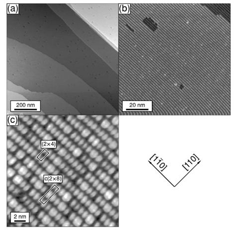
7 Figure 2.
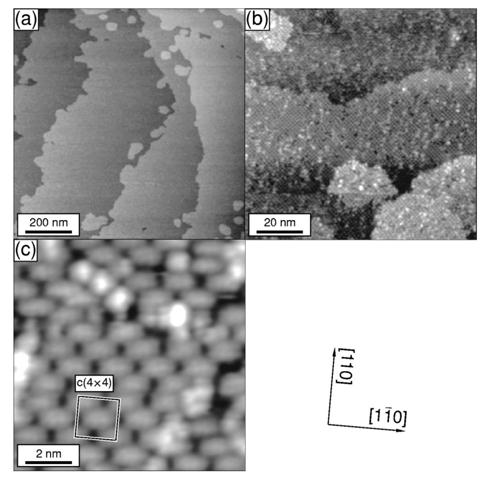
8 Figure 3.
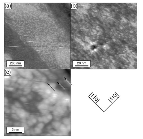
9 Figure 4.
1 Corresponding author:
 Scanning Tunneling Microscopy Study of Cr-doped GaN Surface Grown by RF Plasma Molecular Beam Epitaxy Muhammad B. Haider, Rong Yang, Hamad Al-Brithen, Costel Constantin, Arthur R. Smith 1, Gabriel Caruntu
Structure and Energetics of P-rich GaP(001) Surfaces
 Surfaces") phys. stat. sol. (a) 184, No. 1, 105 110 (2001) Structure and Energetics of P-rich GaP(001) Surfaces O. Pulci 1 ), W. G. Schmidt, and F. Bechstedt Institut für Festkörpertheorie und Theoretische Optik,
phys. stat. sol. (a) 184, No. 1, 105 110 (2001) Structure and Energetics of P-rich GaP(001) Surfaces O. Pulci 1 ), W. G. Schmidt, and F. Bechstedt Institut für Festkörpertheorie und Theoretische Optik,
Surface phase diagram of 2Ã4 and 4Ã2 reconstructions of GaAs 001
 PHYSICAL REVIEW B VOLUME 62, NUMBER 12 15 SEPTEMBER 2000-II Surface phase diagram of 2Ã4 and 4Ã2 reconstructions of GaAs 001 W. G. Schmidt* and S. Mirbt Fysiska Institutionen, Uppsala Universitet, Box
Cross-Section Scanning Tunneling Microscopy of InAs/GaSb Superlattices
 Cross-Section Scanning Tunneling Microscopy of InAs/GaSb Superlattices Cecile Saguy A. Raanan, E. Alagem and R. Brener Solid State Institute. Technion, Israel Institute of Technology, Haifa 32000.Israel
Surface Morphology of GaN Surfaces during Molecular Beam Epitaxy Abstract Introduction
 Surface Morphology of GaN Surfaces during Molecular Beam Epitaxy R. M. Feenstra, Huajie Chen, V. Ramachandran, and C. D. Lee Department of Physics, Carnegie Mellon University, Pittsburgh, Pennsylvania
GaP 001 and InP 001 : Reflectance anisotropy and surface geometry
 GaP 001 and InP 001 : Reflectance anisotropy and surface geometry N. Esser Institut für Festkörperphysik, Technische Universität Berlin, Hardenbergstrasse 36, 10623 Berlin, Germany W. G. Schmidt and J.
LOW-TEMPERATURE Si (111) HOMOEPITAXY AND DOPING MEDIATED BY A MONOLAYER OF Pb
 HOMOEPITAXY AND DOPING MEDIATED BY A MONOLAYER OF Pb") LOW-TEMPERATURE Si (111) HOMOEPITAXY AND DOPING MEDIATED BY A MONOLAYER OF Pb O.D. DUBON, P.G. EVANS, J.F. CHERVINSKY, F. SPAEPEN, M.J. AZIZ, and J.A. GOLOVCHENKO Division of Engineering and Applied Sciences,
LOW-TEMPERATURE Si (111) HOMOEPITAXY AND DOPING MEDIATED BY A MONOLAYER OF Pb O.D. DUBON, P.G. EVANS, J.F. CHERVINSKY, F. SPAEPEN, M.J. AZIZ, and J.A. GOLOVCHENKO Division of Engineering and Applied Sciences,
Indium incorporation and surface segregation during InGaN growth by molecular beam epitaxy: experiment and theory
 Indium incorporation and surface segregation during InGaN growth by molecular beam epitaxy: experiment and theory Huajie Chen 1,1 R. M. Feenstra 1, J. E. Northrup 2, J. Neugebauer 3, and D. W. Greve 4
Study of interface asymmetry in InAs GaSb heterojunctions
 Study of interface asymmetry in InAs GaSb heterojunctions M. W. Wang, D. A. Collins, and T. C. McGill T. J. Watson, Sr. Laboratory of Applied Physics, California Institute of Technology, Pasadena, California
Nanostructure Fabrication Using Selective Growth on Nanosize Patterns Drawn by a Scanning Probe Microscope
 Nanostructure Fabrication Using Selective Growth on Nanosize Patterns Drawn by a Scanning Probe Microscope Kentaro Sasaki, Keiji Ueno and Atsushi Koma Department of Chemistry, The University of Tokyo,
Plan for Lectures #4, 5, & 6. Theme Of Lectures: Nano-Fabrication
 Plan for Lectures #4, 5, & 6 Theme Of Lectures: Nano-Fabrication Quantum Wells, SLs, Epitaxial Quantum Dots Carbon Nanotubes, Semiconductor Nanowires Self-assembly and Self-organization Two Approaches
Structure of InAs/AlSb/InAs resonant tunneling diode interfaces
 Structure of InAs/AlSb/InAs resonant tunneling diode interfaces B. Z. Nosho a) and W. H. Weinberg Center for Quantized Electronic Structures and Department of Chemical Engineering, University of California,
Direct observation of a Ga adlayer on a GaN(0001) surface by LEED Patterson inversion. Xu, SH; Wu, H; Dai, XQ; Lau, WP; Zheng, LX; Xie, MH; Tong, SY
 surface by LEED Patterson inversion. Xu, SH; Wu, H; Dai, XQ; Lau, WP; Zheng, LX; Xie, MH; Tong, SY") Title Direct observation of a Ga adlayer on a GaN(0001) surface by LEED Patterson inversion Author(s) Xu, SH; Wu, H; Dai, XQ; Lau, WP; Zheng, LX; Xie, MH; Tong, SY Citation Physical Review B - Condensed
Title Direct observation of a Ga adlayer on a GaN(0001) surface by LEED Patterson inversion Author(s) Xu, SH; Wu, H; Dai, XQ; Lau, WP; Zheng, LX; Xie, MH; Tong, SY Citation Physical Review B - Condensed
Pb thin films on Si(111): Local density of states and defects
: Local density of states and defects") University of Wollongong Research Online Australian Institute for Innovative Materials - Papers Australian Institute for Innovative Materials 2014 Pb thin films on Si(111): Local density of states and
University of Wollongong Research Online Australian Institute for Innovative Materials - Papers Australian Institute for Innovative Materials 2014 Pb thin films on Si(111): Local density of states and
Reflectance-difference spectroscopy of mixed arsenic-rich phases of gallium arsenide 001
 PHYSICAL REVIEW B VOLUME 62, NUMBER 12 15 SEPTEMBER 2000-II Reflectance-difference spectroscopy of mixed arsenic-rich phases of gallium arsenide 001 M. J. Begarney, 1 L. Li, 2 C. H. Li, 1 D. C. Law, 1
Imaging Methods: Scanning Force Microscopy (SFM / AFM)
") Imaging Methods: Scanning Force Microscopy (SFM / AFM) The atomic force microscope (AFM) probes the surface of a sample with a sharp tip, a couple of microns long and often less than 100 Å in diameter.
Imaging Methods: Scanning Force Microscopy (SFM / AFM) The atomic force microscope (AFM) probes the surface of a sample with a sharp tip, a couple of microns long and often less than 100 Å in diameter.
C. D. Lee and R. M. Feenstra Dept. Physics, Carnegie Mellon University, Pittsburgh, PA 15213
 Morphology and surface reconstructions of GaN(1 1 00) surfaces C. D. Lee and R. M. Feenstra Dept. Physics, Carnegie Mellon University, Pittsburgh, PA 15213 J. E. Northrup Palo Alto Research Center, 3333
SUPPLEMENTARY INFORMATION
 DOI: 10.1038/NCHEM.2491 Experimental Realization of Two-dimensional Boron Sheets Baojie Feng 1, Jin Zhang 1, Qing Zhong 1, Wenbin Li 1, Shuai Li 1, Hui Li 1, Peng Cheng 1, Sheng Meng 1,2, Lan Chen 1 and
Observation of Bulk Defects by Scanning Tunneling Microscopy and Spectroscopy: Arsenic Antisite Defects in GaAs
 VOLUME 71, NUMBER 8 PH YSICAL REVI EW LETTERS 23 AUGUST 1993 Observation of Bulk Defects by Scanning Tunneling Microscopy and Spectroscopy: Arsenic Antisite Defects in GaAs R. M. Feenstra, J. M. Woodall,
JARA FIT Ferienprakticum Nanoelektronik Experiment: Resonant tunneling in quantum structures
 JARA FIT Ferienprakticum Nanoelektronik 2013 Experiment: Resonant tunneling in quantum structures Dr. Mihail Ion Lepsa, Peter Grünberg Institut (PGI 9), Forschungszentrum Jülich GmbH 1. Introduction The
Optimizing Graphene Morphology on SiC(0001)
") Optimizing Graphene Morphology on SiC(0001) James B. Hannon Rudolf M. Tromp Graphene sheets Graphene sheets can be formed into 0D,1D, 2D, and 3D structures Chemically inert Intrinsically high carrier mobility
Optimizing Graphene Morphology on SiC(0001) James B. Hannon Rudolf M. Tromp Graphene sheets Graphene sheets can be formed into 0D,1D, 2D, and 3D structures Chemically inert Intrinsically high carrier mobility
Structure analysis: Electron diffraction LEED TEM RHEED
 Structure analysis: Electron diffraction LEED: Low Energy Electron Diffraction SPA-LEED: Spot Profile Analysis Low Energy Electron diffraction RHEED: Reflection High Energy Electron Diffraction TEM: Transmission
In situ electron-beam processing for III-V semiconductor nanostructure fabrication
 In situ electron-beam processing for III-V semiconductor nanostructure fabrication Tomonori Ishikawa a), Shigeru Kohmoto, Tetsuya Nishimura*, and Kiyoshi Asakawa The Femtosecond Technology Research Association
Scanning Tunneling Microscopy Studies of the Ge(111) Surface
 Surface") VC Scanning Tunneling Microscopy Studies of the Ge(111) Surface Anna Rosen University of California, Berkeley Advisor: Dr. Shirley Chiang University of California, Davis August 24, 2007 Abstract: This
VC Scanning Tunneling Microscopy Studies of the Ge(111) Surface Anna Rosen University of California, Berkeley Advisor: Dr. Shirley Chiang University of California, Davis August 24, 2007 Abstract: This
Currently, worldwide major semiconductor alloy epitaxial growth is divided into two material groups.
 ICQNM 2014 Currently, worldwide major semiconductor alloy epitaxial growth is divided into two material groups. Cubic: Diamond structures: group IV semiconductors (Si, Ge, C), Cubic zinc-blende structures:
Atomic structure of the GaAs 001-2Ã4 surface under As flux
 PHYSICAL REVIEW B, VOLUME 65, 165315 Atomic structure of the GaAs 001-2Ã4 surface under As flux Akihiro Ohtake* Joint Research Center for Atom Technology (JRCAT), Tsukuba 305-0046, Japan and National Institute
Crystalline Surfaces for Laser Metrology
 Crystalline Surfaces for Laser Metrology A.V. Latyshev, Institute of Semiconductor Physics SB RAS, Novosibirsk, Russia Abstract: The number of methodological recommendations has been pronounced to describe
Novel Growth of IngaAs/GaAs Nanostructures by Molecular Beam Epitaxy
 Utah State University DigitalCommons@USU All Graduate Theses and Dissertations Graduate Studies 5-2009 Novel Growth of IngaAs/GaAs Nanostructures by Molecular Beam Epitaxy Dong Jun Kim Utah State University
Hydrogen termination following Cu deposition on Si(001)
") Hydrogen termination following Cu deposition on Si(001) L. A. Baker, A. R. Laracuente,* and L. J. Whitman Naval Research Laboratory, Washington, DC 20375-5342, USA Received 9 September 2004; published
Hydrogen termination following Cu deposition on Si(001) L. A. Baker, A. R. Laracuente,* and L. J. Whitman Naval Research Laboratory, Washington, DC 20375-5342, USA Received 9 September 2004; published
Ultramicroscopy 73 (1998) Received 7 July 1997; received in revised form 10 November 1997
 Received 7 July 1997; received in revised form 10 November 1997") Ultramicroscopy 73 (1998) 229 235 Atomic structure of In As/GaAs(0 0 1) (2 4) and (3 2) surfaces L. Li *, B.K. Han, R.F. Hicks, H. Yoon, M.S. Goorsky Chemical Engineering Department, University of California,
Ultramicroscopy 73 (1998) 229 235 Atomic structure of In As/GaAs(0 0 1) (2 4) and (3 2) surfaces L. Li *, B.K. Han, R.F. Hicks, H. Yoon, M.S. Goorsky Chemical Engineering Department, University of California,
Stripes developed at the strong limit of nematicity in FeSe film
 Stripes developed at the strong limit of nematicity in FeSe film Wei Li ( ) Department of Physics, Tsinghua University IASTU Seminar, Sep. 19, 2017 Acknowledgements Tsinghua University Prof. Qi-Kun Xue,
Direct Observation of Nodes and Twofold Symmetry in FeSe Superconductor
 www.sciencemag.org/cgi/content/full/332/6036/1410/dc1 Supporting Online Material for Direct Observation of Nodes and Twofold Symmetry in FeSe Superconductor Can-Li Song, Yi-Lin Wang, Peng Cheng, Ye-Ping
Wurtzite GaN surface structures studied by scanning tunneling microscopy and reflection high energy electron diffraction
 Wurtzite GaN surface structures studied by scanning tunneling microscopy and reflection high energy electron diffraction A. R. Smith, a) V. Ramachandran, and R. M. Feenstra Department of Physics, Carnegie
Magic numbers in Ga clusters on GaAs (0 0 1) surface
 surface") Journal of Crystal Growth 209 (2000) 258}262 Magic numbers in Ga clusters on GaAs (0 0 1) surface Shiro Tsukamoto*, Nobuyuki Koguchi National Research Institute for Metals, 1-2-1 Sengen, Tsukuba, Ibaraki
Journal of Crystal Growth 209 (2000) 258}262 Magic numbers in Ga clusters on GaAs (0 0 1) surface Shiro Tsukamoto*, Nobuyuki Koguchi National Research Institute for Metals, 1-2-1 Sengen, Tsukuba, Ibaraki
Supplementary Figure 1 Experimental setup for crystal growth. Schematic drawing of the experimental setup for C 8 -BTBT crystal growth.
 Supplementary Figure 1 Experimental setup for crystal growth. Schematic drawing of the experimental setup for C 8 -BTBT crystal growth. Supplementary Figure 2 AFM study of the C 8 -BTBT crystal growth
MICRO-FOUR-POINT PROBES IN A UHV SCANNING ELECTRON MICROSCOPE FOR IN-SITU SURFACE-CONDUCTIVITY MEASUREMENTS
 Surface Review and Letters, Vol. 7, Nos. 5 & 6 (2000) 533 537 c World Scientific Publishing Company MICRO-FOUR-POINT PROBES IN A UHV SCANNING ELECTRON MICROSCOPE FOR IN-SITU SURFACE-CONDUCTIVITY MEASUREMENTS
X-ray photoelectron spectroscopy investigation of the mixed anion GaSb/lnAs heterointerface
 X-ray photoelectron spectroscopy investigation of the mixed anion GaSb/lnAs heterointerface M. W. Wang, D. A. Collins, and T. C. McGill T. J. Watson, Sr., Laboratory of Applied Physics, California Institute
ABSTRACT INTRODUCTION
 Mat. Res. Soc. Symp. Proc. Vol. 696 22 Materials Research Society Surface reconstruction and induced uniaxial magnetic fields on Ni films R. A. Lukaszew, B. McNaughton 1, V. Stoica 2 and R. Clarke 2 Department
Nanoprobing of semiconductor heterointerfaces: quantum dots, alloys and diffusion
 INSTITUTE OF PHYSICS PUBLISHING JOURNAL OF PHYSICS D: APPLIED PHYSICS J. Phys. D: Appl. Phys. 37 (24) R163 R178 PII: S22-3727(4)37445- TOPICAL REVIEW Nanoprobing of semiconductor heterointerfaces: quantum
Inversion of wurtzite GaN(0001) by exposure to magnesium
 by exposure to magnesium") Inversion of wurtzite GaN(0001) by exposure to magnesium V. Ramachandran and R. M. Feenstra Department of Physics, Carnegie Mellon University, Pittsburgh, PA 15213 W. L. Sarney and L. Salamanca-Riba Materials
Inversion of wurtzite GaN(0001) by exposure to magnesium V. Ramachandran and R. M. Feenstra Department of Physics, Carnegie Mellon University, Pittsburgh, PA 15213 W. L. Sarney and L. Salamanca-Riba Materials
Physics and Material Science of Semiconductor Nanostructures
 Physics and Material Science of Semiconductor Nanostructures PHYS 570P Prof. Oana Malis Email: omalis@purdue.edu Course website: http://www.physics.purdue.edu/academic_programs/courses/phys570p/ Lecture
Surface Defects on Natural MoS 2
 Supporting Information: Surface Defects on Natural MoS 2 Rafik Addou 1*, Luigi Colombo 2, and Robert M. Wallace 1* 1 Department of Materials Science and Engineering, The University of Texas at Dallas,
Fabrication and Domain Imaging of Iron Magnetic Nanowire Arrays
 Abstract #: 983 Program # MI+NS+TuA9 Fabrication and Domain Imaging of Iron Magnetic Nanowire Arrays D. A. Tulchinsky, M. H. Kelley, J. J. McClelland, R. Gupta, R. J. Celotta National Institute of Standards
Spontaneous lateral composition modulation in InAlAs and InGaAs short-period superlattices
 Physica E 2 (1998) 325 329 Spontaneous lateral composition modulation in InAlAs and InGaAs short-period superlattices D.M. Follstaedt *, R.D. Twesten, J. Mirecki Millunchick, S.R. Lee, E.D. Jones, S.P.
Morphology and surface reconstructions of m-plane GaN
 Morphology and surface reconstructions of m-plane GaN C. D. Lee, 1 R. M. Feenstra, 1 J. E. Northrup, 2 L. Lymperakis, 3 J. Neugebauer 3 1 Department of Physics, Carnegie Mellon University, Pittsburgh,
Supporting Information
 Supporting Information Defects and Surface Structural Stability of MoTe 2 Under Vacuum Annealing Hui Zhu, Qingxiao Wang, Lanxia Cheng, Rafik Addou, Jiyoung Kim, Moon J. Kim*, Robert M. Wallace* Department
Surface morphologies associated with thermal desorption: Scanning tunneling microscopy studies of Br GaAs(110)
") Surface morphologies associated with thermal desorption: Scanning tunneling microscopy studies of Br GaAs(110) C. Y. Cha, J. Brake, B. Y. Han, D. W. Owens, and J. H. Weaver a) Department of Materials Science
Surface morphologies associated with thermal desorption: Scanning tunneling microscopy studies of Br GaAs(110) C. Y. Cha, J. Brake, B. Y. Han, D. W. Owens, and J. H. Weaver a) Department of Materials Science
Review of Structure of Bare and Adsorbate-Covered GaN(0001) Surfaces
 Surfaces") M RS Internet Journal Nitride Semiconductor Research Review of Structure of Bare and Adsorbate-Covered GaN(0001) Surfaces R. M. Feenstra 1, J. E. Northrup 2 and Jörg Neugebauer 3 1 Department of Physics,
M RS Internet Journal Nitride Semiconductor Research Review of Structure of Bare and Adsorbate-Covered GaN(0001) Surfaces R. M. Feenstra 1, J. E. Northrup 2 and Jörg Neugebauer 3 1 Department of Physics,
Cross-sectional scanning tunneling microscopy of InAsSb/InAsP superlattices
 Cross-sectional scanning tunneling microscopy of InAsSb/InAsP superlattices S. L. Zuo and E. T. Yu a) Department of Electrical and Computer Engineering, University of California at San Diego, La Jolla,
Nanostructure. Materials Growth Characterization Fabrication. More see Waser, chapter 2
 Nanostructure Materials Growth Characterization Fabrication More see Waser, chapter 2 Materials growth - deposition deposition gas solid Physical Vapor Deposition Chemical Vapor Deposition Physical Vapor
In order to determine the energy level alignment of the interface between cobalt and
 SUPPLEMENTARY INFORMATION Energy level alignment of the CuPc/Co interface In order to determine the energy level alignment of the interface between cobalt and CuPc, we have performed one-photon photoemission
Atomic structure and optical anisotropy of III V 001 surfaces
 Atomic structure and optical anisotropy of III V 001 surfaces N. Esser a) Institut für Festkörperphysik, Technische Universität Berlin, Hardenbergstraße 36, 10623 Berlin, Germany W. G. Schmidt IFTO, Friedrich-Schiller-Universtität
Interaction of Hydrogen and Methane with InP(100) and GaAs(100) Surfaces
 and GaAs(100) Surfaces") F. Stietz et al.: Interaction of H and Methane with InP and GaAs Surfaces 185 phys. stat. sol. (a) 159, 185 (1997) Subject classification: 68.35.Bs; S7.11; S7.12 Interaction of Hydrogen and Methane with
F. Stietz et al.: Interaction of H and Methane with InP and GaAs Surfaces 185 phys. stat. sol. (a) 159, 185 (1997) Subject classification: 68.35.Bs; S7.11; S7.12 Interaction of Hydrogen and Methane with
Intrinsic vacancy induced nanoscale wire structure in heteroepitaxial Ga 2 Se 3 /Si(001)
") Intrinsic vacancy induced nanoscale wire structure in heteroepitaxial Ga 2 Se 3 /Si(001) Taisuke Ohta, 1, D. A. Schmidt, 2 Shuang Meng, 2, A. Klust, 2, A. Bostwick, 2, Q. Yu, 2 Marjorie A. Olmstead, 2
Intrinsic vacancy induced nanoscale wire structure in heteroepitaxial Ga 2 Se 3 /Si(001) Taisuke Ohta, 1, D. A. Schmidt, 2 Shuang Meng, 2, A. Klust, 2, A. Bostwick, 2, Q. Yu, 2 Marjorie A. Olmstead, 2
Structure of Bare and Adsorbate-Covered GaN(0001) Surfaces
 Surfaces") Structure of Bare and Adsorbate-Covered GaN(0001) Surfaces R. M. Feenstra Carnegie Mellon University Department of Physics Pittsburgh, PA 15213, USA. J. E. Northrup Palo Alto Research Center, Inc. 3333
Structure of Bare and Adsorbate-Covered GaN(0001) Surfaces R. M. Feenstra Carnegie Mellon University Department of Physics Pittsburgh, PA 15213, USA. J. E. Northrup Palo Alto Research Center, Inc. 3333
CHAPTER 5 ATOMIC HYDROGEN
 CHAPTER 5 TEMPERATURE DEPENDENT ETCHING OF THE DIAMOND (100) SURFACE BY ATOMIC HYDROGEN 5.1 Introduction Described in previous chapters of this dissertation are the results of the initial UHV STM studies
Ordering of Nanostructures in a Si/Ge 0.3 Si 0.7 /Ge System during Molecular Beam Epitaxy
 Semiconductors, Vol. 36, No. 11, 22, pp. 1294 1298. Translated from Fizika i Tekhnika Poluprovodnikov, Vol. 36, No. 11, 22, pp. 1379 1383. Original Russian Text Copyright 22 by Cirlin, Egorov, Sokolov,
Ga-rich GaAs(001) surfaces observed during high-temperature annealing. by scanning tunneling microscopy
 surfaces observed during high-temperature annealing. by scanning tunneling microscopy") Ga-rich GaAs(001) surfaces observed during high-temperature annealing by scanning tunneling microscopy Shiro Tsukamoto a), Markus Pristovsek, Bradford G. Orr b), Akihiro Ohtake, Gavin R. Bell c), and Nobuyuki
Ga-rich GaAs(001) surfaces observed during high-temperature annealing by scanning tunneling microscopy Shiro Tsukamoto a), Markus Pristovsek, Bradford G. Orr b), Akihiro Ohtake, Gavin R. Bell c), and Nobuyuki
A constant potential of 0.4 V was maintained between electrodes 5 and 6 (the electrode
 (a) (b) Supplementary Figure 1 The effect of changing po 2 on the field-enhanced conductance A constant potential of 0.4 V was maintained between electrodes 5 and 6 (the electrode configuration is shown
Studies of Iron-Based Superconductor Thin Films
 MBE Growth and STM Studies of Iron-Based Superconductor Thin Films Wei Li 1, Canli Song 1,2, Xucun Ma 2, Xi Chen 1*, Qi-Kun Xu 1 State Key Laboratory of Low-Dimensional Quantum Physics, Department of Physics,
Surface termination during GaN growth by metal-organic vapor phase epitaxy determined by ellipsometry. Abstract
 HEP/123-qed Surface termination during GaN growth by metal-organic vapor phase epitaxy determined by ellipsometry C. Cobet, T. Schmidtling, M. Drago, N. Wollschläger, N. Esser, and W. Richter Institut
Extreme band bending at MBE-grown InAs(0 0 1) surfaces induced by in situ sulphur passivation
 surfaces induced by in situ sulphur passivation") Journal of Crystal Growth 237 239 (2002) 196 200 Extreme band bending at MBE-grown InAs(0 0 1) surfaces induced by in situ sulphur passivation M.J. Lowe a, T.D. Veal a, C.F. McConville a, G.R. Bell b,
Journal of Crystal Growth 237 239 (2002) 196 200 Extreme band bending at MBE-grown InAs(0 0 1) surfaces induced by in situ sulphur passivation M.J. Lowe a, T.D. Veal a, C.F. McConville a, G.R. Bell b,
Intersubband Transitions in Narrow InAs/AlSb Quantum Wells
 Intersubband Transitions in Narrow InAs/AlSb Quantum Wells D. C. Larrabee, J. Tang, M. Liang, G. A. Khodaparast, J. Kono Department of Electrical and Computer Engineering, Rice Quantum Institute, and Center
2D MBE Activities in Sheffield. I. Farrer, J. Heffernan Electronic and Electrical Engineering The University of Sheffield
 2D MBE Activities in Sheffield I. Farrer, J. Heffernan Electronic and Electrical Engineering The University of Sheffield Outline Motivation Van der Waals crystals The Transition Metal Di-Chalcogenides
In-situ ellipsometry: Identification of surface terminations during GaN growth
 In-situ ellipsometry: Identification of surface terminations during GaN growth C. Cobet 1, T. Schmidtling 1, M. Drago 1, N. Wollschläger 1, N. Esser 1, W. Richter 1, and R. M. Feenstra 2 1 Institut für
Grazing Incidence Fast Atom Diffraction: a new tool for surface characterization
 Grazing Incidence Fast Atom Diffraction: a new tool for surface characterization Victor H. Etgens Institut des NanoSciences de Paris Outline Introduction GIFAD : technique how it works; Experimental set-up;
Special Properties of Au Nanoparticles
 Special Properties of Au Nanoparticles Maryam Ebrahimi Chem 7500/750 March 28 th, 2007 1 Outline Introduction The importance of unexpected electronic, geometric, and chemical properties of nanoparticles
Chapter 103 Spin-Polarized Scanning Tunneling Microscopy
 Chapter 103 Spin-Polarized Scanning Tunneling Microscopy Toyo Kazu Yamada Keywords Spin-polarized tunneling current Spin polarization Magnetism 103.1 Principle Spin-polarized scanning tunneling microscopy
Growth optimization of InGaAs quantum wires for infrared photodetector applications
 Growth optimization of InGaAs quantum wires for infrared photodetector applications Chiun-Lung Tsai, Chaofeng Xu, K. C. Hsieh, and K. Y. Cheng a Department of Electrical and Computer Engineering and Micro
Assessment of Structural Properties of InAs/GaSb Superlattice by Double Crystal X-Ray Diffraction and Cross-Sectional Scanning Tunnelling Microscopy
 Bulg. J. Phys. 31 (2004) 204 212 Assessment of Structural Properties of InAs/GaSb Superlattice by Double Crystal X-Ray Diffraction and Cross-Sectional Scanning Tunnelling Microscopy O. Maksimov 1, J. Steinshnider
Site seectivity in the initial oxidation of the Si 111-7=7 surface
 Applied Surface Science 126 1998 317 322 ž / Site seectivity in the initial oxidation of the Si 111-7=7 surface Jeong Sook Ha a,), Kang-Ho Park a, El-Hang Lee a, Seong-Ju Park b a Research Department,
Electrical properties of InSb quantum wells remotely doped with Si
 Electrical properties of InSb quantum wells remotely doped with Si K. J. Goldammer, a) W. K. Liu, b) G. A. Khodaparast, S. C. Lindstrom, M. B. Johnson, R. E. Doezema, and M. B. Santos Laboratory for Electronic
Low-temperature Scanning Tunneling Spectroscopy of Semiconductor Surfaces
 Low-temperature Scanning Tunneling Spectroscopy of Semiconductor Surfaces R. M. Feenstra 1 Department of Physics, Carnegie Mellon University, Pittsburgh, Pennsylvania 15213 G. Meyer 2 Paul Drude Institut
Step-induced electronic resonance at vicinal Si(001) observed by spectroscopic SHG and RAS
 observed by spectroscopic SHG and RAS") Step-induced electronic resonance at vicinal Si(001) observed by spectroscopic SHG and RAS Robert Ehlert, Jinhee Kwon and Michael C. Downer Department of Physics, The University of Texas at Austin, Austin
Step-induced electronic resonance at vicinal Si(001) observed by spectroscopic SHG and RAS Robert Ehlert, Jinhee Kwon and Michael C. Downer Department of Physics, The University of Texas at Austin, Austin
TMT4320 Nanomaterials November 10 th, Thin films by physical/chemical methods (From chapter 24 and 25)
") 1 TMT4320 Nanomaterials November 10 th, 2015 Thin films by physical/chemical methods (From chapter 24 and 25) 2 Thin films by physical/chemical methods Vapor-phase growth (compared to liquid-phase growth)
1 TMT4320 Nanomaterials November 10 th, 2015 Thin films by physical/chemical methods (From chapter 24 and 25) 2 Thin films by physical/chemical methods Vapor-phase growth (compared to liquid-phase growth)
Magic nanoclusters of group III metals on Si(100) surface
 surface") e-journal of Surface Science and Nanotechnology 27 May 2003 e-j. Surf. Sci. Nanotech. Vol. 1 (2003) 33-40 Magic nanoclusters of group III metals on Si(100) surface Review Paper V. G. Kotlyar 1, A. V. Zotov
e-journal of Surface Science and Nanotechnology 27 May 2003 e-j. Surf. Sci. Nanotech. Vol. 1 (2003) 33-40 Magic nanoclusters of group III metals on Si(100) surface Review Paper V. G. Kotlyar 1, A. V. Zotov
Self-Assembled InAs Quantum Dots
 Self-Assembled InAs Quantum Dots Steve Lyon Department of Electrical Engineering What are semiconductors What are semiconductor quantum dots How do we make (grow) InAs dots What are some of the properties
Temperature Dependent Current-voltage Characteristics of P- type Crystalline Silicon Solar Cells Fabricated Using Screenprinting
 Temperature Dependent Current-voltage Characteristics of P- type Crystalline Silicon Solar Cells Fabricated Using Screenprinting Process Hyun-Jin Song, Won-Ki Lee, Chel-Jong Choi* School of Semiconductor
Solid Surfaces, Interfaces and Thin Films
 Hans Lüth Solid Surfaces, Interfaces and Thin Films Fifth Edition With 427 Figures.2e Springer Contents 1 Surface and Interface Physics: Its Definition and Importance... 1 Panel I: Ultrahigh Vacuum (UHV)
Lecture 30: Kinetics of Epitaxial Growth: Surface Diffusion and
 Lecture 30: Kinetics of Epitaxial Growth: Surface Diffusion and Nucleation Today s topics Understanding the basics of epitaxial techniques used for surface growth of crystalline structures (films, or layers).
solidi current topics in solid state physics InAs quantum dots grown by molecular beam epitaxy on GaAs (211)B polar substrates
B polar substrates") solidi status physica pss c current topics in solid state physics InAs quantum dots grown by molecular beam epitaxy on GaAs (211)B polar substrates M. Zervos1, C. Xenogianni1,2, G. Deligeorgis1, M. Androulidaki1,
solidi status physica pss c current topics in solid state physics InAs quantum dots grown by molecular beam epitaxy on GaAs (211)B polar substrates M. Zervos1, C. Xenogianni1,2, G. Deligeorgis1, M. Androulidaki1,
A general rule for surface reconstructions of III V semiconductors
 Surface Science 422 (1999) L177 L182 Surface Science Letters A general rule for surface reconstructions of III V semiconductors S. Mirbt a,*, N. Moll b, A. Kley b, J.D. Joannopoulos a a Department of Physics,
Size-selected Metal Cluster Deposition on Oxide Surfaces: Impact Dynamics and Supported Cluster Chemistry
 Size-selected Metal Cluster Deposition on Oxide Surfaces: Impact Dynamics and Supported Cluster Chemistry Sungsik Lee, Masato Aizawa, Chaoyang Fan, Tianpin Wu, and Scott L. Anderson Support: AFOSR, DOE
SUPPLEMENTARY INFORMATION
 SUPPLEMENTARY INFORMATION Towards wafer-size graphene layers by atmospheric pressure graphitization of silicon carbide Supporting online material Konstantin V. Emtsev 1, Aaron Bostwick 2, Karsten Horn
The Structure of GaSb Digitally Doped with Mn
 The Structure of GaSb Digitally Doped with Mn G. I. Boishin a,, J. M. Sullivan a,b,,* and L. J. Whitman a,* a Naval Research Laboratory, Washington, DC 20375 b Northwestern University, Evanston, IL 20208
Investigation of the bonding strength and interface current of p-siõn-gaas wafers bonded by surface activated bonding at room temperature
 Investigation of the bonding strength and interface current of p-siõn-gaas wafers bonded by surface activated bonding at room temperature M. M. R. Howlader, a) T. Watanabe, and T. Suga Research Center
Growth and nonlinear optical properties of GaAs absorber layers for AlGaAsÕCaF 2 semiconductor saturable absorber mirrors
 Growth and nonlinear optical properties of GaAs absorber layers for AlGaAsÕCaF 2 semiconductor saturable absorber mirrors S. Schön, a) M. Haiml, M. Achermann, and U. Keller Institute of Quantum Electronics,
G. L. KELLOGG. Sandia National Laboratories Albuquerque, NM USA. 1. Abstract
 ' C' 54NB 9s - q27 r, coup -C/606222-- AN ATOMC VEW OF CLUSTER DFFUSON ON METAL SURFACES G. L. KELLOGG Sandia National Laboratories Albuquerque, NM 8785-43 USA. Abstract Field ion microscope measurements
Low Temperature (LT), Ultra High Vacuum (UHV LT) Scanning Probe Microscopy (SPM) Laboratory
, Ultra High Vacuum (UHV LT) Scanning Probe Microscopy (SPM) Laboratory") Low Temperature (LT), Ultra High Vacuum (UHV LT) Scanning Probe Microscopy (SPM) Laboratory The laboratory of Low Temperature, Ultra High Vacuum (UHV LT) is specifically designed for surface science microscopy
Low Temperature (LT), Ultra High Vacuum (UHV LT) Scanning Probe Microscopy (SPM) Laboratory The laboratory of Low Temperature, Ultra High Vacuum (UHV LT) is specifically designed for surface science microscopy
Structure of Clean and Arsenic-covered GaN(0001) Surfaces
 Surfaces") Structure of Clean and Arsenic-covered GaN(0001) Surfaces V. Ramachandran, C. D. Lee, and R. M. Feenstra Department of Physics, Carnegie Mellon University, Pittsburgh, Pennsylvania 15213 A. R. Smith Department
Structure of Clean and Arsenic-covered GaN(0001) Surfaces V. Ramachandran, C. D. Lee, and R. M. Feenstra Department of Physics, Carnegie Mellon University, Pittsburgh, Pennsylvania 15213 A. R. Smith Department
Sponsored by. Contract No. N K-0073: Modification P00006 DARPA Order 5674 NR
 OTIC FILE COP Study of Interfacial Chemistry between Metals and Their Effects on Electronic Systems q. o Sponsored by 00 Defense Advanced Research Projects Agency (DOD) and The Office of Naval Research
Effect of Spiral Microwave Antenna Configuration on the Production of Nano-crystalline Film by Chemical Sputtering in ECR Plasma
 THE HARRIS SCIENCE REVIEW OF DOSHISHA UNIVERSITY, VOL. 56, No. 1 April 2015 Effect of Spiral Microwave Antenna Configuration on the Production of Nano-crystalline Film by Chemical Sputtering in ECR Plasma
Self-organization of quantum-dot pairs by high-temperature
 Nanoscale Res Lett (2006) 1:57 61 DOI 10.1007/s11671-006-9002-z NANO EXPRESS Self-organization of quantum-dot pairs by high-temperature droplet epitaxy Zhiming M. Wang Æ Kyland Holmes Æ Yuriy I. Mazur
Self-Assembled InAs Quantum Dots on Patterned InP Substrates
 Self-Assembled InAs Quantum Dots on Patterned InP Substrates J. Lefebvre, P.J. Poole, J. Fraser, G.C. Aers, D. Chithrani, and R.L. Williams Institute for Microstructural Sciences, National Research Council
Introduction to Semiconductor Physics. Prof.P. Ravindran, Department of Physics, Central University of Tamil Nadu, India
 Introduction to Semiconductor Physics 1 Prof.P. Ravindran, Department of Physics, Central University of Tamil Nadu, India http://folk.uio.no/ravi/cmp2013 Review of Semiconductor Physics Semiconductor fundamentals
Imaging of Quantum Confinement and Electron Wave Interference
 : Forefront of Basic Research at NTT Imaging of Quantum Confinement and lectron Wave Interference Kyoichi Suzuki and Kiyoshi Kanisawa Abstract We investigated the spatial distribution of the local density
Supplementary Information:
 Supplementary Figures Supplementary Information: a b 1 2 3 0 ΔZ (pm) 66 Supplementary Figure 1. Xe adsorbed on a Cu(111) surface. (a) Scanning tunnelling microscopy (STM) topography of Xe layer adsorbed
Strain-induced single-domain growth of epitaxial SrRuO 3 layers on SrTiO 3 : a high-temperature x-ray diffraction study
 Strain-induced single-domain growth of epitaxial SrRuO 3 layers on SrTiO 3 : a high-temperature x-ray diffraction study Arturas Vailionis 1, Wolter Siemons 1,2, Gertjan Koster 1 1 Geballe Laboratory for
New evidence for the influence of step morphology on the formation of Au atomic chains on vicinal Si(111) surfaces
 surfaces") OFFPRINT New evidence for the influence of step morphology on the formation of Au atomic chains on vicinal Si(111) surfaces N. McAlinden and J. F. McGilp EPL, 92 (2010) 67008 Please visit the new website
OFFPRINT New evidence for the influence of step morphology on the formation of Au atomic chains on vicinal Si(111) surfaces N. McAlinden and J. F. McGilp EPL, 92 (2010) 67008 Please visit the new website
ANTIMONY ENHANCED HOMOGENEOUS NITROGEN INCORPORATION INTO GaInNAs FILMS GROWN BY ATOMIC HYDROGEN-ASSISTED MOLECULAR BEAM EPITAXY
 ANTIMONY ENHANCED HOMOGENEOUS NITROGEN INCORPORATION INTO GaInNAs FILMS GROWN BY ATOMIC HYDROGEN-ASSISTED MOLECULAR BEAM EPITAXY Naoya Miyashita 1, Nazmul Ahsan 1, and Yoshitaka Okada 1,2 1. Research Center