Electrical spin injection from ferromagnet into an InAs heterostructures through MgO tunnel barrier
|
|
|
- Gyles Perry
- 5 years ago
- Views:
Transcription
1 Electrical spin injection from ferromagnet into an InAs heterostructures through MgO tunnel barrier T. Ishikura, Z. Cui, L-K. Liefeith, K. Konishi and Kanji Yoh Research center for integrated quantum electronics, Hokkaido university, Sapporo , Japan We have investigated electrical spin injection from Ni 81 Fe 19 into an InAs quantum well through MgO tunneling barrier for potential application to InAs-based spin field effect transistor. Injected spin polarized current were detected in both nonlocal and local spin valve set-ups and the spin diffusion length and spin injection efficiency were analyzed. The spin diffusion length was estimated to be 1.6 μm in nonlocal set-up at 1.4 K. The spin polarization of Ni 81 Fe 19 /MgO/InAs as-deposited sample was relealed to be 6.9 %, while increased spin polarization of 8.9 % was observed by additional thermal treatment.
2 Semiconductor spintronics has a potential of providing alternative logic scheme to overcome a limitation of conventional Si VLSI technology. 1-4 For improving the Spin-field effect transistor (FET) characteristics, high spin injection efficiency and strong spin orbit (SO) interactions are desirable. So far a number of spin injection and detection in ferromagnetic metal/semiconductor hybrid structures have been examined in various methods, such as circular polarization detection from spin light emitting diode 5-6, electrical spin accumulation detection in nonlocal geometry 7-9 and so on. Among them, nonlocal spin valve measurement has been widely used for electrical spin injection and detection measurements which is free from the influence of anisotropic magnetic resistance (AMR) and local Hall effect. Moreover, conductivity mismatch at the interface of FM and semiconductors (SC) is one of the obstacles for suppressing spin injection efficiency in case of zero electric field at the interface. 10 This can be overcome by using either Schottky barrier or tunneling barrier near FMs/SC interface, which have been investigated in various FM/SC materials 11. Optimized control of the contact resistance plays a crucial role for efficient spin injection and detection. In those circumstances, InAs heterostructure is a good candidate to investigate the spin injection dependence on the contact resistance by changing the tunneling barrier thickness because it is well known that the Fermi level is pinned inside conduction band. On the other hand, for gate control of the channel spin state is another issue to achieve spin transistor. For this purpose, InAs is known to be a good candidate material for spin channel in a Datta-Das spin transistor for its high spin orbit interaction The band offset and carrier distribution was found to affect the Rashba SOI strength strongly and gate electric field in InAlAs/InGaAs metamorphic heterostructures make it possible to control it Thus, the FM/MgO/InAs structure has been selectedas a suitable materials system in order to investigate the advantages of MgO tunnel barrier on spin injection from FM into narrow gap semiconductors. In this letter, we show local and nonlocal spin injection from NiFe spin injector into an InAs
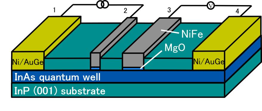
3 heterostructures through MgO tunnel barrier and investigated the spin diffusion length and spin injection efficiency dependence on various structures. We have fabricated the local and nonlocal spin injection devices based on an InAs-based inverted high electron mobility transisistor (HEMT) structure grown on semi-insulating InP (001) substrate. The 4.1 nm InAs channel layer of the HEMT is buried in the middle of InGaAs sub-channel layer to confirm mobility and increased SO interaction. The structure consist of 300/800 nm of InP/ In 0.52 Al 0.48 As buffer layer, cm -2 of Si δ-doping, 10 nm of In 0.52 Al 0.48 As spacer layer, 5.6 nm of In 0.53 Ga 0.47 As sub-channel, 4.1 nm of InAs main channel, 1.8 nm of In 0.53 Ga 0.47 As sub-channel, 50 nm of In 0.52 Al 0.48 As barrier layer and In 0.53 Ga 0.47 As 10 nm cap-layer. The electrical transport parameters were characterized by Hall measurement, yielding 20,000 cm 2 /Vs of mobility, cm -2 of carrier density and 300 Ohm/ of sheet resistance at 1.4 K. The SO interaction strength was observed to evm at 1.4 K determined by Shubnikov-de Haas oscillation and its waveform analysis by Maximum Entropy Method of Fast Fourier Transform (FFT). The channel of 50 μm width was constructed by wet chemical etching aligned along [110] direction. The FM electrode patterns for a spin injector and a detector were defined to be 0.2 and 0.4 μm widths using electron beam lithography. The Ni 81 Fe 19 (70 nm)/mgo (2 nm) stack was deposited by electron beam evaporator on InAs channel directly after wet chemical etching of top barrier layers. After lift-off, a part of the sample was subjected to annealing at 250 C for 40 min in ultra high vacuum chamber for the purpose of MgO crystalline quality improvement. Then, the contact resistance area product (RA) of the ferromagnetic electrode to the InAs channel was controlled by MgO thickness and annealing treatment. The measured RA without anneal were Ωcm 2 and Ωcm 2 for non-annealed and with annealed samples characterized by 4-terminal measurement method, indicating that the annealing process reduced leakage current. The increase of contact resistance
4 may have been caused by decrease of anti-site defects in MgO by the thermal treatment. These resistance values are sufficient for achieving appreciable spin injection based on conductivity mismatch theory R s ch=r s L sd /W where R s is the sheet resistance, L sd is the spin diffusion length and W is the channel width. 21 Spin valve measurements were conducted in local and nonlocal configurations at 1.4 K as shown in Figure 1. The nonlocal voltage was measured between electrodes 3 and 4, whereas the constant current of 100 μa was run between terminals 2 and 1. The magnetic field was swept parallel and anti-parallel to the longitudinal direction of NiFe electrodes. In Figure 2, typical nonlocal (a) and local (b) measurement results are shown. The spacing of terminals 2 and 3 of the nonlocal measurement was 0.7µm. The clear voltage peaks were obtained at 100 Gauss and at -100 Gauss upon positive and negative sweeps of the external magnetic field, respectively. Additionally, local measurement results are shown in Fig.2 (b). Its resistance peaks are seen to coincide with the nonlocal measurement shown in Fig.2 (a). The magnetoresistance (MR) ratio was estimated to be 0.2 %, which is 6 times higher than nonlocal voltage signals. In Fig.3, the R NL (V NL /I) and MR ( R AP -R P /R P ) ratio are shown as a function of L. Spin polarization at the injection point, η, and spin diffusion length, L sd, were estimated by fitting the data with the formula R NL =(η I η D R s L sd /W)exp(L/L sd ), where η is the spin polarization of spin injector and detector and L sd is spin diffusion length. The estimated spin polarization and spin diffusion length for the non-annealed sample were 6.9 % and 1.6 μm, respectively and annealed sample, they were 8.9 % and 0.73 μm, respectively. To the best of our knowledge, it is the highest electrical spin injection from ferromagnet into InAs channel. Additionally, the spin life time τ S was estimated to be 8.0 ps from τ S =L 2 sd /D, where diffusion constant, D, was substituted by the extracted value from Hall-effect measurements assuming that it is independent of spin polarization. Unfortunately, it is not possible to compare this estimation of τ S =8.0 ps with Hanle
5 measurements because the Hanle signal of the present sample was below detection level within 1k Gauss scan. This result seems reasonable because estimated magnetic field of the Hanle half-width would amount to 4 T if we use τ S =8.0 ps value and the formula τ S =h/(2πgμ B B), where h is Plank constant, g is effective electron g-factor, μ B is Bohr magnetron and B is perpendicular magnetic field against substrate. Thus, it is obvious that we can never obtain τ S with Hanle measurement without changing the magnetization directions from in-plane to perpendicular direction because 4 T is twice as high as vertical saturation magnetization (hard axis) of the ferromagnetic electrode The MR magnitude is theoretically estimated from contact resistance. When the contact resistance is dominated by tunnel resistance, MR ratio is described as follows MR 1 2 L R 2cosh ch b L s sd R ch R s ch R b sinh L ch L sd. (1), where R b =R P /(2(1-η 2 )). This relationship predicts maximum MR signal when R b equals to R s ch, the normalized channel resistance. Following equation (1), MR dependence on R b of the non-annealed and annealed samples are plotted in Fig.4 based upon nonlocal spin valve measurement results. For the non-annealed sample, our experimental data exhibited an MR ratio of 0.2 % with a contact resistivity of Ωcm 2 and L ch =700 nm,whereas the annealed sample showed an MR ratio below 0.02 % with a contact resistivity of Ωcm 2 and L ch =1µm. This explains why local measurement signal of the annealed sample was below detection level. Both MR ratios are in good agreement with the previous calculation. Both improvement of spin injection efficiency (8.9%) and increased tunneling resistance (3x10⁻⁴ Ωcm 2 ) of the annealed sample suggest that the annealing process improved the crystalline quality of e-beam evaporated MgO tunnel layer.
6 In summary, we have demonstrated spin injection efficiency of 8.9 % in NiFe/MgO/InAs structure in nonlocal spin valves measurements. Non-annealed samples showed spin injection efficiency of 6.9 % and 5.7 % by nonlocal and local measurements, respectively. The enhancement of spin injection efficiency from 6.9 % to 8.9 % by annealing is presumably due to the improvement of e-beam evaporated MgO crystal quality upon annealing. Measured value of local MR agreed reasonably well with the estimation based on nonlocal measurements. Acknowledgement This work was partly supported by Strategic International Research Cooperative Program, Japan Science and Technology Agency (JST).
7 References 1 S. Datta and B. Das, Appl. Phys. Lett. 56, 665 (1990). 2 P. Bruno and J. Wunderlich, J. Appl. Phys. 84, 978 (1998). 3 A. F. Morpurgo, J. P. Heida, T. M. Klapwijk, B. J. van Wees and G. Borghs, Phys. Rev. Lett (1998). 4 S. Sugahara and M. Tanaka, Appl. Phys. Lett. 84, 2307 (2004). 5 H. J. Zhu, M. Ramsteiner, H. Kostial, M. Wassermeier, H. P. Schonherr, and K.H. Ploog, Phys. Rev. Lett. 87, (2001). 6 K. Yoh, H. Ohno, K. Sueoka, and M. E. Ramsteiner, J. Vac. Sci. Technol. B 22, 1432 (2004). 7 H. C. Koo, H. Yi, J. B. Ko, J. Chang, S. H Han, D. Jung, S. G. Huh and J. Eom, Appl. Phys. Lett 90, (2007). 8 X. Lou, C. Adelmann, S. A. Crooker, E. S. Garlid, J. Zhang, K. S. M. Reddy, S. D. Flexner, C. J. Palmstrom and P. A. Crowell, Nature Physics 31, 197 (2007). 9 T. Sasaki, T. Oikawa, T. Suzuki, M. Shiraishi, Y. Suzuki, and K. Tagami, Appl. Phys. Express 2, (2009). 10 G. Schmidt, D. Ferrand, L. W. Mollenkamp, A. T. Fillip and B. J. van Wees, Phys. Rev. B 62, R4790 (2000). 11 E. I. Rashba, Phys Rev, B 62, R (2000). 12 I. Žutić, J. Fabian and S. D. Sarma, Rev. Mod. Phys. 76, 323 (2004). 13 J. Schliemann, J. C. Egues and D. Ross, Phys. Rev. Lett. 90, (2003). 14 R. Winkler, Phys. Rev. B 69, (2004). 15 M. Ohno and K. Yoh, Phys. Rev. B 75, (R) (2007). 16 P. Pfeffer and W. Zawadzki, Phys. Rev. B 68, (2003). 17 J. Nitta, T. Akazaki, H. Takayanagi, and T. Enoki, Phys. Rev. Lett. 78, 1335 (1997).
8 18 T. Matsuda and K. Yoh, Physica E 42, 979 (2010). 19 T. Matsuda and K. Yoh, J. Electron. Mater. 37, 1806 (2008). 20 H. C. Koo, J. H. Kwon, J. Eom, J. Chang, S. H. Han and M. Johnson, Science 325, 1515 (2009). 21 F. Magnus, S. K. Clowes, A. M. Gilbertson, W. R. Branford, E. D. Barkhoudarov, L. F. Cohena, L. J. Singh, Z. H. Barber, M. G. Blamire, P. D. Buckle, L. Buckle, T. Ashley, D. A. Eustace and D. W. McComb, Appl. Phys. Lett. 91, (2007). 22 B. Dlubak, M. B. Martin, C. Deranlot, B. Servet, S. Xavier, R. Mattana, M. Sprinkle, C. Berger, W. De Heer, F. Petroff, A. Anane1, P. Seneor and A. Fert, Nature Physics 8, 557 (2012).
9 Figure captions FIG. 1. Schematic diagram of four-terminal lateral spin valves. The wide channel of 50µm was formed by wet chemical etching. After the top barrier layers were etched down to the InAs channel layer, NiFe/MgO were stacked. The width of the spin injector and detector (NiFe/MgO) were to be 0.2 and 0.4 μm. For spin valve measurements, the magnetic field was swept in long distance (1-10) direction of the electrodes. Nonlocal voltage was detected between 3 and 4, while constant current was biased form 2 to 1. The local resistance was detected between 2 and 3. FIG. 2. Typical spin valve characteristics in nonlocal geometry (a) and local geometry (b) in L=0.7 μm at 1.4 K. The current was fixed to 100 μa for nonlocal and 1 ma for local measurements. The closed circle (open circle) represents positive (negative) direction sweep of the external magnetic field along the longitudinal axis of FM electrodes. FIG. 3. The spin valve signals as a function of FM electrode spacing, L, in nonlocal geometry (a) and local geometry (b) at 1.4 K. The dotted line indicates the exponential decay fit. (c) The spin valve signals of the annealed samples and its exponential decay fit. (L sd =1.6 μm) FIG. 4. The MR ratio as a function of contact resistance of the non-annealed (square) and annealed samples (circle). The values of theoretical calculation were indicated by solid line for non-annealed and dotted line for annealed samples, respectively.
10 FIG. 1
11 FIG. 2
12 FIG. 3
13 FIG. 4
Room-Temperature Electron Spin Transport in a Highly Doped Si Channel. AIT, Akita Research Institute of Advanced Technology, Akita , Japan
 Room-Temperature Electron Spin Transport in a Highly Doped Si Channel Toshio Suzuki*, Tomoyuki Sasaki 1, Tohru Oikawa 1, Masashi Shiraishi, Yoshishige Suzuki, and Kiyoshi Noguchi 1 AIT, Akita Research
Temperature dependence of spin diffusion length in silicon by Hanle-type spin. precession
 Temperature dependence of spin diffusion length in silicon by Hanle-type spin precession T. Sasaki 1,a), T. Oikawa 1, T. Suzuki 2, M. Shiraishi 3, Y. Suzuki 3, and K. Noguchi 1 SQ Research Center, TDK
Anisotropic spin splitting in InGaAs wire structures
 Available online at www.sciencedirect.com Physics Physics Procedia Procedia 3 (010) 00 (009) 155 159 000 000 14 th International Conference on Narrow Gap Semiconductors and Systems Anisotropic spin splitting
Spin injection. concept and technology
 Spin injection concept and technology Ron Jansen ャンセンロン Spintronics Research Center National Institute of Advanced Industrial Science and Technology (AIST), Tsukuba, Japan Spin injection Transfer of spin
Saroj P. Dash. Chalmers University of Technology. Göteborg, Sweden. Microtechnology and Nanoscience-MC2
 Silicon Spintronics Saroj P. Dash Chalmers University of Technology Microtechnology and Nanoscience-MC2 Göteborg, Sweden Acknowledgement Nth Netherlands University of Technology Sweden Mr. A. Dankert Dr.
Citation for published version (APA): Filip, A. T. (2002). Spin polarized electron transport in mesoscopic hybrid devices s.n.
: Filip, A. T. (2002). Spin polarized electron transport in mesoscopic hybrid devices s.n.") University of Groningen Spin polarized electron transport in mesoscopic hybrid devices Filip, Andrei Teodor IMPORTANT NOTE: You are advised to consult the publisher's version (publisher's PDF) if you wish
University of Groningen Spin polarized electron transport in mesoscopic hybrid devices Filip, Andrei Teodor IMPORTANT NOTE: You are advised to consult the publisher's version (publisher's PDF) if you wish
All-electrical measurements of direct spin Hall effect in GaAs with Esaki diode electrodes.
 All-electrical measurements of direct spin Hall effect in GaAs with Esaki diode electrodes. M. Ehlert 1, C. Song 1,2, M. Ciorga 1,*, M. Utz 1, D. Schuh 1, D. Bougeard 1, and D. Weiss 1 1 Institute of Experimental
Semiconductor Spintronics
 Semiconductor Spintronics Junsaku Nitta Abstract In semiconductor spintronics, electron spin rather than charge is the key property. This paper describes several spin-related devices using spin-orbit interaction.
ConceptGraphene. Small or medium-scale focused research project. WP4 Spin transport devices
 ConceptGraphene New Electronics Concept: Wafer-Scale Epitaxial Graphene Small or medium-scale focused research project WP4 Spin transport devices Deliverable 4.1 Report on spin transport in graphene on
TRANSVERSE SPIN TRANSPORT IN GRAPHENE
 International Journal of Modern Physics B Vol. 23, Nos. 12 & 13 (2009) 2641 2646 World Scientific Publishing Company TRANSVERSE SPIN TRANSPORT IN GRAPHENE TARIQ M. G. MOHIUDDIN, A. A. ZHUKOV, D. C. ELIAS,
Enhancement of spin relaxation time in hydrogenated graphene spin-valve devices Wojtaszek, M.; Vera-Marun, I. J.; Maassen, T.
 University of Groningen Enhancement of spin relaxation time in hydrogenated graphene spin-valve devices Wojtaszek, M.; Vera-Marun, I. J.; Maassen, T.; van Wees, Bart Published in: Physical Review. B: Condensed
Current-driven Magnetization Reversal in a Ferromagnetic Semiconductor. (Ga,Mn)As/GaAs/(Ga,Mn)As Tunnel Junction
As/GaAs/(Ga,Mn)As Tunnel Junction") Current-driven Magnetization Reversal in a Ferromagnetic Semiconductor (Ga,Mn)As/GaAs/(Ga,Mn)As Tunnel Junction D. Chiba 1, 2*, Y. Sato 1, T. Kita 2, 1, F. Matsukura 1, 2, and H. Ohno 1, 2 1 Laboratory
Current-driven Magnetization Reversal in a Ferromagnetic Semiconductor (Ga,Mn)As/GaAs/(Ga,Mn)As Tunnel Junction D. Chiba 1, 2*, Y. Sato 1, T. Kita 2, 1, F. Matsukura 1, 2, and H. Ohno 1, 2 1 Laboratory
United Nations Educational, Scientific and Cultural Organization and International Atomic Energy Agency
 Available at: http://publications.ictp.it IC/2010/033 United Nations Educational, Scientific and Cultural Organization and International Atomic Energy Agency THE ABDUS SALAM INTERNATIONAL CENTRE FOR THEORETICAL
A spin Esaki diode. Makoto Kohda, Yuzo Ohno, Koji Takamura, Fumihiro Matsukura, and Hideo Ohno. Abstract
 A spin Esaki diode Makoto Kohda, Yuzo Ohno, Koji Takamura, Fumihiro Matsukura, and Hideo Ohno Laboratory for Electronic Intelligent Systems, Research Institute of Electrical Communication, Tohoku University,
Title. Author(s) 石倉, 丈継. Issue Date DOI. Doc URL. Type. File Information. Electrical spin injection from ferromagnet into an I
 石倉, 丈継. Issue Date DOI. Doc URL. Type. File Information. Electrical spin injection from ferromagnet into an I") Title Electrical spin injection from ferromagnet into an I Author(s) 石倉, 丈継 Issue Date 2015-03-25 DOI 10.14943/doctoral.k11753 Doc URL http://hdl.handle.net/2115/58800 Type theses (doctoral) File Information
Title Electrical spin injection from ferromagnet into an I Author(s) 石倉, 丈継 Issue Date 2015-03-25 DOI 10.14943/doctoral.k11753 Doc URL http://hdl.handle.net/2115/58800 Type theses (doctoral) File Information
Datta-Das type spin-field effect transistor in non-ballistic regime
 Datta-Das type spin-field effect transistor in non-ballistic regime Munekazu Ohno 1, Kanji Yoh 1,2 1 Research Center for Integrated Quantum Electronics, Hokkaido University, Sapporo, 060-8628, Japan 2
SUPPLEMENTARY INFORMATION
 SUPPLEMENTARY INFORMATION DOI: 10.1038/NNANO.2014.16 Electrical detection of charge current-induced spin polarization due to spin-momentum locking in Bi 2 Se 3 by C.H. Li, O.M.J. van t Erve, J.T. Robinson,
Electrical detection of spin transport in lateral ferromagnet semiconductor devices
 Electrical detection of spin transport in lateral ferromagnet semiconductor devices XIAOHUA LOU 1, CHRISTOPH ADELMANN 2, SCOTT A. CROOKER 3,ERICS.GARLID 1, JIANJIE ZHANG 1, K. S. MADHUKAR REDDY 2, SOREN
Effects of Quantum-Well Inversion Asymmetry on Electron- Nuclear Spin Coupling in the Fractional Quantum Hall Regime
 Effects of Quantum-Well Inversion Asymmetry on Electron- Nuclear Spin Coupling in the Fractional Quantum Hall Regime Katsushi Hashimoto,,2,a Koji Muraki,,b Norio Kumada, Tadashi Saku, 3 and Yoshiro Hirayama,2
Surfaces, Interfaces, and Layered Devices
 Surfaces, Interfaces, and Layered Devices Building blocks for nanodevices! W. Pauli: God made solids, but surfaces were the work of Devil. Surfaces and Interfaces 1 Interface between a crystal and vacuum
Ferroelectric Field Effect Transistor Based on Modulation Doped CdTe/CdMgTe Quantum Wells
 Vol. 114 (2008) ACTA PHYSICA POLONICA A No. 5 Proc. XXXVII International School of Semiconducting Compounds, Jaszowiec 2008 Ferroelectric Field Effect Transistor Based on Modulation Doped CdTe/CdMgTe Quantum
Akabori, Masashi; Hidaka, Shiro; Yam Author(s) Kozakai, Tomokazu; Matsuda, Osamu; Y. Japanese Journal of Applied Physics,
 Kozakai, Tomokazu; Matsuda, Osamu; Y. Japanese Journal of Applied Physics,") JAIST Reposi https://dspace.j Title High-In-content InGaAs quantum point fabricated using focused ion beam sy with N_2 gas field ion source Akabori, Masashi; Hidaka, Shiro; Yam Author(s) Kozakai, Tomokazu;
JAIST Reposi https://dspace.j Title High-In-content InGaAs quantum point fabricated using focused ion beam sy with N_2 gas field ion source Akabori, Masashi; Hidaka, Shiro; Yam Author(s) Kozakai, Tomokazu;
Spin Injection into a Graphene Thin Film at Room Temperature
 Spin Injection into a Graphene Thin Film at Room Temperature Megumi Ohishi, Masashi Shiraishi*, Ryo Nouchi, Takayuki Nozaki, Teruya Shinjo, and Yoshishige Suzuki Graduate School of Engineering Science,
Mesoscopic Spintronics
 Mesoscopic Spintronics Taro WAKAMURA (Université Paris-Sud) Lecture 1 Today s Topics 1.1 History of Spintronics 1.2 Fudamentals in Spintronics Spin-dependent transport GMR and TMR effect Spin injection
Max-Planck-Institut für Metallforschung Stuttgart. Towards Spin Injection into Silicon. Saroj Prasad Dash. Dissertation an der Universität Stuttgart
 Max-Planck-Institut für Metallforschung Stuttgart Towards Spin Injection into Silicon Saroj Prasad Dash Dissertation an der Universität Stuttgart Bericht Nr. 203 August 2007 Towards Spin Injection into
Current mechanisms Exam January 27, 2012
 Current mechanisms Exam January 27, 2012 There are four mechanisms that typically cause currents to flow: thermionic emission, diffusion, drift, and tunneling. Explain briefly which kind of current mechanisms
Universal valence-band picture of. the ferromagnetic semiconductor GaMnAs
 Universal valence-band picture of the ferromagnetic semiconductor GaMnAs Shinobu Ohya *, Kenta Takata, and Masaaki Tanaka Department of Electrical Engineering and Information Systems, The University of
Theory of electrical spin injection: Tunnel contacts as a solution of the conductivity mismatch problem
 Theory of electrical spin injection: Tunnel contacts as a solution of the conductivity mismatch problem The Harvard community has made this article openly available. Please share how this access benefits
Electrical spin-injection into semiconductors
 Electrical spin-injection into semiconductors L. W. Molenkamp Physikalisches Institut Universität Würzburg Am Hubland 97074 Würzburg Germany Contents Motivation The usual approach Theoretical treatment
All-Electrical Spin Field Effect Transistor in van der Waals Heterostructures at Room Temperature
 All-Electrical Spin Field Effect Transistor in van der Waals Heterostructures at Room Temperature André Dankert*, Saroj P. Dash Department of Microtechnology and Nanoscience, Chalmers University of Technology,
Influence of surface treatment and interface layers on electrical spin injection efficiency and transport in InAs
 Influence of surface treatment and interface layers on electrical spin injection efficiency and transport in InAs L. Zhu and E. T. Yu a Department of Electrical and Computer Engineering, Microelectronics
arxiv: v3 [cond-mat.mtrl-sci] 11 Aug 2008
![arxiv: v3 [cond-mat.mtrl-sci] 11 Aug 2008](/thumbs/71/65777543.jpg "arxiv: v3 [cond-mat.mtrl-sci] 11 Aug 2008") Non-ohmic spin transport in n-type doped silicon Hyuk-Jae Jang, Jing Xu, Jing Li, Biqin Huang, and Ian Appelbaum Department of Electrical and Computer Engineering, University of Delaware, Newark, Delaware,
Non-ohmic spin transport in n-type doped silicon Hyuk-Jae Jang, Jing Xu, Jing Li, Biqin Huang, and Ian Appelbaum Department of Electrical and Computer Engineering, University of Delaware, Newark, Delaware,
Spin-valve Effect in Nanoscale Si-based Devices
 DOI: 10.22661/AAPPSBL.2018.28.3.07 Spin-valve Effect in Nanoscale Si-based Devices Duong Dinh Hiep 1, Masaaki Tanaka 2,3 and Pham Nam Hai 1,3 1 Department of Electrical and Electronic Engineering, Tokyo
Fundamental concepts of spintronics
 Fundamental concepts of spintronics Jaroslav Fabian Institute for Theoretical Physics University of Regensburg Stara Lesna, 24. 8. 2008 SFB 689 :outline: what is spintronics? spin injection spin-orbit
Spin injection and the local Hall effect in InAs quantum wells
 Spin injection and the local Hall effect in InAs quantum wells F.G. Monzon * and M.L. Roukes California Institute of Technology, Condensed Matter Physics 114-36, Pasadena CA 91125 We report on our efforts
Low-dimensional electron transport properties in InAs/AlGaSb mesoscopic structures
 Superlattices and Microstructures, Vol 21, No 1, 1997 Low-dimensional electron transport properties in InAs/AlGaSb mesoscopic structures M Inoue, T Sugihara, T Maemoto, S Sasa, H Dobashi, S Izumiya Department
Spin pumping in Ferromagnet-Topological Insulator-Ferromagnet Heterostructures Supplementary Information.
 Spin pumping in Ferromagnet-Topological Insulator-Ferromagnet Heterostructures Supplementary Information. A.A. Baker,, 2 A.I. Figueroa, 2 L.J. Collins-McIntyre, G. van der Laan, 2 and T., a) Hesjedal )
Electrical spin injection and detection of spin precession in room temperature bulk GaN lateral spin valves
 Electrical spin injection and detection of spin precession in room temperature bulk GaN lateral spin valves Aniruddha Bhattacharya a), Md Zunaid Baten a) and Pallab Bhattacharya a) a) Center for Photonic
Zeeman splitting of single semiconductor impurities in resonant tunneling heterostructures
 Superlattices and Microstructures, Vol. 2, No. 4, 1996 Zeeman splitting of single semiconductor impurities in resonant tunneling heterostructures M. R. Deshpande, J. W. Sleight, M. A. Reed, R. G. Wheeler
Physics of Semiconductors
 Physics of Semiconductors 13 th 2016.7.11 Shingo Katsumoto Department of Physics and Institute for Solid State Physics University of Tokyo Outline today Laughlin s justification Spintronics Two current
Traps in MOCVD n-gan Studied by Deep Level Transient Spectroscopy and Minority Carrier Transient Spectroscopy
 Traps in MOCVD n-gan Studied by Deep Level Transient Spectroscopy and Minority Carrier Transient Spectroscopy Yutaka Tokuda Department of Electrical and Electronics Engineering, Aichi Institute of Technology,
SPINTRONICS. Waltraud Buchenberg. Faculty of Physics Albert-Ludwigs-University Freiburg
 SPINTRONICS Waltraud Buchenberg Faculty of Physics Albert-Ludwigs-University Freiburg July 14, 2010 TABLE OF CONTENTS 1 WHAT IS SPINTRONICS? 2 MAGNETO-RESISTANCE STONER MODEL ANISOTROPIC MAGNETO-RESISTANCE
Spin injection in ferromagnet-semiconductor heterostructures at room temperature invited
 JOURNAL OF APPLIED PHYSICS VOLUME 91, NUMBER 10 15 MAY 2002 Spin injection in ferromagnet-semiconductor heterostructures at room temperature invited Klaus H. Ploog a) Paul Drude Institute for Solid State
Hall Effect. Sergio O. Valenzuela. ICREA and Centre d Investigació en Nanociència i Nanotecnologia (ICN-CSIC), Barcelona.
, Barcelona.") Nonlocal Spin Detection and the Spin Hall Effect Sergio O. Valenzuela Sergio.Valenzuela.icn@uab.es ICREA and Centre d Investigació en Nanociència i Nanotecnologia (ICN-CSIC), Barcelona CEMAG 2009 Zaragoza,
Nonlocal Spin Detection and the Spin Hall Effect Sergio O. Valenzuela Sergio.Valenzuela.icn@uab.es ICREA and Centre d Investigació en Nanociència i Nanotecnologia (ICN-CSIC), Barcelona CEMAG 2009 Zaragoza,
Magnon-drag thermopile
 Magnon-drag thermopile I. DEVICE FABRICATION AND CHARACTERIZATION Our devices consist of a large number of pairs of permalloy (NiFe) wires (30 nm wide, 20 nm thick and 5 µm long) connected in a zigzag
File name: Supplementary Information Description: Supplementary Figures and Supplementary References. File name: Peer Review File Description:
 File name: Supplementary Information Description: Supplementary Figures and Supplementary References File name: Peer Review File Description: Supplementary Figure Electron micrographs and ballistic transport
Segmented 1.55um Laser with 400% Differential Quantum Efficiency J. Getty, E. Skogen, L. Coldren, University of California, Santa Barbara, CA.
 Segmented 1.55um Laser with 400% Differential Quantum Efficiency J. Getty, E. Skogen, L. Coldren, University of California, Santa Barbara, CA. Abstract: By electrically segmenting, and series-connecting
NONLINEAR TRANSPORT IN BALLISTIC SEMICONDUCTOR DIODES WITH NEGATIVE EFFECTIVE MASS CARRIERS
 NONLINEAR TRANSPORT IN BALLISTIC SEMICONDUCTOR DIODES WITH NEGATIVE EFFECTIVE MASS CARRIERS B. R. Perkins, Jun Liu, and A. Zaslavsky, Div. of Engineering Brown University Providence, RI 02912, U.S.A.,
Observation of the intrinsic inverse spin Hall effect in Ni 80 Fe 20. Yuichiro Ando, Teruya Shinjo and Masashi Shiraishi * #
 Observation of the intrinsic inverse spin Hall effect in Ni 80 Fe 20 Ayaka Tsukahara #, Yuta Kitamura #, Eiji Shikoh, Yuichiro Ando, Teruya Shinjo and Masashi Shiraishi * # Graduate School of Engineering
GaAs and InGaAs Single Electron Hex. Title. Author(s) Kasai, Seiya; Hasegawa, Hideki. Citation 13(2-4): Issue Date DOI
 Kasai, Seiya; Hasegawa, Hideki. Citation 13(2-4): Issue Date DOI") Title GaAs and InGaAs Single Electron Hex Circuits Based on Binary Decision D Author(s) Kasai, Seiya; Hasegawa, Hideki Citation Physica E: Low-dimensional Systems 3(2-4): 925-929 Issue Date 2002-03 DOI
Title GaAs and InGaAs Single Electron Hex Circuits Based on Binary Decision D Author(s) Kasai, Seiya; Hasegawa, Hideki Citation Physica E: Low-dimensional Systems 3(2-4): 925-929 Issue Date 2002-03 DOI
SUPPLEMENTARY INFORMATION
 Dirac electron states formed at the heterointerface between a topological insulator and a conventional semiconductor 1. Surface morphology of InP substrate and the device Figure S1(a) shows a 10-μm-square
Performance Analysis of Ultra-Scaled InAs HEMTs
 Purdue University Purdue e-pubs Birck and NCN Publications Birck Nanotechnology Center 2009 Performance Analysis of Ultra-Scaled InAs HEMTs Neerav Kharche Birck Nanotechnology Center and Purdue University,
Metallic: 2n 1. +n 2. =3q Armchair structure always metallic = 2
 Properties of CNT d = 2.46 n 2 2 1 + n1n2 + n2 2π Metallic: 2n 1 +n 2 =3q Armchair structure always metallic a) Graphite Valence(π) and Conduction(π*) states touch at six points(fermi points) Carbon Nanotube:
Spin and charge transport in material with spin-dependent conductivity
 Spin and charge transport in material with -dependent conductivity V.Zayets Spintronic Research Center, National Institute of Advanced Industrial Science and Technology (AIST), Umezono 1-1-1, Tsukuba,
From nanophysics research labs to cell phones. Dr. András Halbritter Department of Physics associate professor
 From nanophysics research labs to cell phones Dr. András Halbritter Department of Physics associate professor Curriculum Vitae Birth: 1976. High-school graduation: 1994. Master degree: 1999. PhD: 2003.
Formation of unintentional dots in small Si nanostructures
 Superlattices and Microstructures, Vol. 28, No. 5/6, 2000 doi:10.1006/spmi.2000.0942 Available online at http://www.idealibrary.com on Formation of unintentional dots in small Si nanostructures L. P. ROKHINSON,
Mapping the potential within a nanoscale undoped GaAs region using. a scanning electron microscope
 Mapping the potential within a nanoscale undoped GaAs region using a scanning electron microscope B. Kaestner Microelectronics Research Centre, Cavendish Laboratory, University of Cambridge, Madingley
Enhancing the Performance of Organic Thin-Film Transistor using a Buffer Layer
 Proceedings of the 9th International Conference on Properties and Applications of Dielectric Materials July 19-23, 29, Harbin, China L-7 Enhancing the Performance of Organic Thin-Film Transistor using
Intrinsic Electronic Transport Properties of High. Information
 Intrinsic Electronic Transport Properties of High Quality and MoS 2 : Supporting Information Britton W. H. Baugher, Hugh O. H. Churchill, Yafang Yang, and Pablo Jarillo-Herrero Department of Physics, Massachusetts
Advanced Lab Course. Tunneling Magneto Resistance
 Advanced Lab Course Tunneling Magneto Resistance M06 As of: 015-04-01 Aim: Measurement of tunneling magnetoresistance for different sample sizes and recording the TMR in dependency on the voltage. Content
Fabrication and Measurement of Spin Devices. Purdue Birck Presentation
 Fabrication and Measurement of Spin Devices Zhihong Chen School of Electrical and Computer Engineering Birck Nanotechnology Center, Discovery Park Purdue University Purdue Birck Presentation zhchen@purdue.edu
HYSWITCH Informal meeting Chersonissos - Crete September 15th 19th 2007,
 HYSWITCH Informal meeting Chersonissos - Crete September 15th 19th 27, Scuola Normale Superiore & NEST CNR-INFM I-56126 Pisa, Italy F. Carillo I. Batov G. Biasiol F. Deon F. Dolcini F. Giazotto V. Pellegrini
High Temperature Ferromagnetism in GaAs-based Heterostructures. with Mn Delta Doping
 High Temperature Ferromagnetism in GaAs-based Heterostructures with Mn Delta Doping A. M. Nazmul, 1,2 T. Amemiya, 1 Y. Shuto, 1 S. Sugahara, 1 and M. Tanaka 1,2 1. Department of Electronic Engineering,
Impact of disorder and topology in two dimensional systems at low carrier densities
 Impact of disorder and topology in two dimensional systems at low carrier densities A Thesis Submitted For the Degree of Doctor of Philosophy in the Faculty of Science by Mohammed Ali Aamir Department
Bias dependent inversion of tunneling magnetoresistance. in Fe/GaAs/Fe tunnel junctions
 Bias dependent inversion of tunneling magnetoresistance in Fe/GaAs/Fe tunnel junctions J. Moser, M. Zenger, C. Gerl, D. Schuh, R. Meier, P. Chen, G. Bayreuther, W. Wegscheider, and D. Weiss Institut für
Observation of electric current induced by optically injected spin current
 1 Observation of electric current induced by optically injected spin current Xiao-Dong Cui 1,2*, Shun-Qing Shen 1,3*, Jian Li 1, Weikun Ge 4, Fu-Chun Zhang 1,3 1 Department of Physics, The University of
Landau quantization, Localization, and Insulator-quantum. Hall Transition at Low Magnetic Fields
 Landau quantization, Localization, and Insulator-quantum Hall Transition at Low Magnetic Fields Tsai-Yu Huang a, C.-T. Liang a, Gil-Ho Kim b, C.F. Huang c, C.P. Huang a and D.A. Ritchie d a Department
Supplementary Figure S1. AFM images of GraNRs grown with standard growth process. Each of these pictures show GraNRs prepared independently,
 Supplementary Figure S1. AFM images of GraNRs grown with standard growth process. Each of these pictures show GraNRs prepared independently, suggesting that the results is reproducible. Supplementary Figure
introduction: what is spin-electronics?
 Spin-dependent transport in layered magnetic metals Patrick Bruno Max-Planck-Institut für Mikrostrukturphysik, Halle, Germany Summary: introduction: what is spin-electronics giant magnetoresistance (GMR)
5 Magnetic Sensors Introduction Theory. Applications
 Sensor devices Magnetic sensors Outline 5 Magnetic Sensors Introduction Theory GalvanomagneticG Effects Applications Introduction A magnetic sensor is a transducer that converts a magnetic field into an
Recent developments in spintronic
 Recent developments in spintronic Tomas Jungwirth nstitute of Physics ASCR, Prague University of Nottingham in collaboration with Hitachi Cambridge, University of Texas, Texas A&M University - Spintronics
Normally-Off GaN Field Effect Power Transistors: Device Design and Process Technology Development
 Center for High Performance Power Electronics Normally-Off GaN Field Effect Power Transistors: Device Design and Process Technology Development Dr. Wu Lu (614-292-3462, lu.173@osu.edu) Dr. Siddharth Rajan
2005 EDP Sciences. Reprinted with permission.
 H. Holmberg, N. Lebedeva, S. Novikov, J. Ikonen, P. Kuivalainen, M. Malfait, and V. V. Moshchalkov, Large magnetoresistance in a ferromagnetic GaMnAs/GaAs Zener diode, Europhysics Letters 71 (5), 811 816
Classification of Solids
 Classification of Solids Classification by conductivity, which is related to the band structure: (Filled bands are shown dark; D(E) = Density of states) Class Electron Density Density of States D(E) Examples
NiCl2 Solution concentration. Etching Duration. Aspect ratio. Experiment Atmosphere Temperature. Length(µm) Width (nm) Ar:H2=9:1, 150Pa
 Width (nm) Ar:H2=9:1, 150Pa") Experiment Atmosphere Temperature #1 # 2 # 3 # 4 # 5 # 6 # 7 # 8 # 9 # 10 Ar:H2=9:1, 150Pa Ar:H2=9:1, 150Pa Ar:H2=9:1, 150Pa Ar:H2=9:1, 150Pa Ar:H2=9:1, 150Pa Ar:H2=9:1, 150Pa Ar:H2=9:1, 150Pa Ar:H2=9:1,
Experiment Atmosphere Temperature #1 # 2 # 3 # 4 # 5 # 6 # 7 # 8 # 9 # 10 Ar:H2=9:1, 150Pa Ar:H2=9:1, 150Pa Ar:H2=9:1, 150Pa Ar:H2=9:1, 150Pa Ar:H2=9:1, 150Pa Ar:H2=9:1, 150Pa Ar:H2=9:1, 150Pa Ar:H2=9:1,
Spin relaxation of conduction electrons Jaroslav Fabian (Institute for Theoretical Physics, Uni. Regensburg)
") Spin relaxation of conduction electrons Jaroslav Fabian (Institute for Theoretical Physics, Uni. Regensburg) :Syllabus: 1. Introductory description 2. Elliott-Yafet spin relaxation and spin hot spots 3.
Spin relaxation of conduction electrons Jaroslav Fabian (Institute for Theoretical Physics, Uni. Regensburg) :Syllabus: 1. Introductory description 2. Elliott-Yafet spin relaxation and spin hot spots 3.
Supporting Online Material for
 www.sciencemag.org/cgi/content/full/327/5966/662/dc Supporting Online Material for 00-GHz Transistors from Wafer-Scale Epitaxial Graphene Y.-M. Lin,* C. Dimitrakopoulos, K. A. Jenkins, D. B. Farmer, H.-Y.
arxiv:cond-mat/ v1 [cond-mat.mes-hall] 3 Feb 1999
![arxiv:cond-mat/ v1 [cond-mat.mes-hall] 3 Feb 1999](/thumbs/88/117721611.jpg "arxiv:cond-mat/ v1 [cond-mat.mes-hall] 3 Feb 1999") An observation of spin-valve effects in a semiconductor field effect transistor: a novel spintronic device. arxiv:cond-mat/99257v1 [cond-mat.mes-hall] 3 Feb 1999 S. Gardelis, C.G Smith, C.H.W. Barnes,
An observation of spin-valve effects in a semiconductor field effect transistor: a novel spintronic device. arxiv:cond-mat/99257v1 [cond-mat.mes-hall] 3 Feb 1999 S. Gardelis, C.G Smith, C.H.W. Barnes,
Persistent spin helix in spin-orbit coupled system. Joe Orenstein UC Berkeley and Lawrence Berkeley National Lab
 Persistent spin helix in spin-orbit coupled system Joe Orenstein UC Berkeley and Lawrence Berkeley National Lab Persistent spin helix in spin-orbit coupled system Jake Koralek, Chris Weber, Joe Orenstein
Quiz #1 Practice Problem Set
 Name: Student Number: ELEC 3908 Physical Electronics Quiz #1 Practice Problem Set? Minutes January 22, 2016 - No aids except a non-programmable calculator - All questions must be answered - All questions
Honors Research Thesis. Engineering at The Ohio State University. Dominic Labanowski Department of Electrical and Computer Engineering
 Imaging Spin Properties using Spatially Varying Magnetic Fields Honors Research Thesis Presented in Partial Fulfillment of the Requirements for the Degree Bachelor of Science with Honors Research Distinction
Optically pumped transport in ferromagnet-semiconductor Schottky diodes invited
 JOURNAL OF APPLIED PHYSICS VOLUME 91, NUMBER 10 15 MAY 2002 Optically pumped transport in ferromagnet-semiconductor Schottky diodes invited A. F. Isakovic School of Physics and Astronomy, University of
Supplementary material: Nature Nanotechnology NNANO D
 Supplementary material: Nature Nanotechnology NNANO-06070281D Coercivities of the Co and Ni layers in the nanowire spin valves In the tri-layered structures used in this work, it is unfortunately not possible
Lecture 9: Metal-semiconductor junctions
 Lecture 9: Metal-semiconductor junctions Contents 1 Introduction 1 2 Metal-metal junction 1 2.1 Thermocouples.......................... 2 3 Schottky junctions 4 3.1 Forward bias............................
SUPPLEMENTARY INFORMATION
 DOI: 10.1038/NPHYS576 Colossal Enhancement of Spin-Orbit Coupling in Weakly Hydrogenated Graphene Jayakumar Balakrishnan 1,, *, Gavin Kok Wai Koon 1,, 3, *, Manu Jaiswal 1,,, Antonio H. Castro Neto 1,,
Electrical Spin injection and Spin transport in semiconducting Si and Ge channels
 Electrical Spin injection and Spin transport in semiconducting Si and Ge channels João Filipe Pires Cunha joao.f.pires.cunha@ist.utl.pt Instituto Superior Técnico, Lisbon, Portugal Under supervision of
An Overview of Spintronics in 2D Materials
 An Overview of Spintronics in 2D Materials Wei Han ( 韩伟 ) 1 2014 ICQM Outline I. Introduction to spintronics (Lecture I) II. Spin injection and detection in 2D (Lecture I) III. Putting magnetic moment
Solid Surfaces, Interfaces and Thin Films
 Hans Lüth Solid Surfaces, Interfaces and Thin Films Fifth Edition With 427 Figures.2e Springer Contents 1 Surface and Interface Physics: Its Definition and Importance... 1 Panel I: Ultrahigh Vacuum (UHV)
Electrostatics of Nanowire Transistors
 Electrostatics of Nanowire Transistors Jing Guo, Jing Wang, Eric Polizzi, Supriyo Datta and Mark Lundstrom School of Electrical and Computer Engineering Purdue University, West Lafayette, IN, 47907 ABSTRACTS
Periodic Magnetoresistance Oscillations in Side-Gated Quantum Dots
 Institute of Physics Publishing Journal of Physics: Conference Series 3 () 11 119 doi:1.1/17-59/3/1/9 NPMS-7/SIMD-5 (Maui 5) Periodic Magnetoresistance Oscillations in Side-Gated Quantum Dots T. Suzuki,
Enhancement-mode quantum transistors for single electron spin
 Purdue University Purdue e-pubs Other Nanotechnology Publications Birck Nanotechnology Center 8-1-2006 Enhancement-mode quantum transistors for single electron spin G. M. Jones B. H. Hu C. H. Yang M. J.
Indium arsenide quantum wire trigate metal oxide semiconductor field effect transistor
 JOURNAL OF APPLIED PHYSICS 99, 054503 2006 Indium arsenide quantum wire trigate metal oxide semiconductor field effect transistor M. J. Gilbert a and D. K. Ferry Department of Electrical Engineering and
Hyperfine Effects in Ferromagnet-Semiconductor Heterostructures
 Hyperfine Effects in Ferromagnet-Semiconductor Heterostructures A DISSERTATION SUBMITTED TO THE FACULTY OF THE GRADUATE SCHOOL OF THE UNIVERSITY OF MINNESOTA BY Mun Keat Chan IN PARTIAL FULFILLMENT OF
MSE 310/ECE 340: Electrical Properties of Materials Fall 2014 Department of Materials Science and Engineering Boise State University
 MSE 310/ECE 340: Electrical Properties of Materials Fall 2014 Department of Materials Science and Engineering Boise State University Practice Final Exam 1 Read the questions carefully Label all figures
Fundamentals of Nanoelectronics: Basic Concepts
 Fundamentals of Nanoelectronics: Basic Concepts Sławomir Prucnal FWIM Page 1 Introduction Outline Electronics in nanoscale Transport Ohms law Optoelectronic properties of semiconductors Optics in nanoscale
Single ion implantation for nanoelectronics and the application to biological systems. Iwao Ohdomari Waseda University Tokyo, Japan
 Single ion implantation for nanoelectronics and the application to biological systems Iwao Ohdomari Waseda University Tokyo, Japan Contents 1.History of single ion implantation (SII) 2.Novel applications
Lecture 20: Semiconductor Structures Kittel Ch 17, p , extra material in the class notes
 Lecture 20: Semiconductor Structures Kittel Ch 17, p 494-503, 507-511 + extra material in the class notes MOS Structure Layer Structure metal Oxide insulator Semiconductor Semiconductor Large-gap Semiconductor
Metal Semiconductor Contacts
 Metal Semiconductor Contacts The investigation of rectification in metal-semiconductor contacts was first described by Braun [33-35], who discovered in 1874 the asymmetric nature of electrical conduction
A HYDROGEN SENSITIVE Pd/GaN SCHOTTKY DIODE SENSOR
 Journal of Physical Science, Vol. 17(2), 161 167, 2006 161 A HYDROGEN SENSITIVE Pd/GaN SCHOTTKY DIODE SENSOR A.Y. Hudeish 1,2* and A. Abdul Aziz 1 1 School of Physics, Universiti Sains Malaysia, 11800
Decay of spin polarized hot carrier current in a quasi. one-dimensional spin valve structure arxiv:cond-mat/ v1 [cond-mat.mes-hall] 10 Oct 2003
![Decay of spin polarized hot carrier current in a quasi. one-dimensional spin valve structure arxiv:cond-mat/ v1 [cond-mat.mes-hall] 10 Oct 2003](/thumbs/74/70335523.jpg "Decay of spin polarized hot carrier current in a quasi. one-dimensional spin valve structure arxiv:cond-mat/ v1 [cond-mat.mes-hall] 10 Oct 2003") Decay of spin polarized hot carrier current in a quasi one-dimensional spin valve structure arxiv:cond-mat/0310245v1 [cond-mat.mes-hall] 10 Oct 2003 S. Pramanik and S. Bandyopadhyay Department of Electrical
Decay of spin polarized hot carrier current in a quasi one-dimensional spin valve structure arxiv:cond-mat/0310245v1 [cond-mat.mes-hall] 10 Oct 2003 S. Pramanik and S. Bandyopadhyay Department of Electrical