Hall Effect. Sergio O. Valenzuela. ICREA and Centre d Investigació en Nanociència i Nanotecnologia (ICN-CSIC), Barcelona.
|
|
|
- Curtis Roy Knight
- 5 years ago
- Views:
Transcription

, Barcelona CEMAG 2009")
1 Nonlocal Spin Detection and the Spin Hall Effect Sergio O. Valenzuela ICREA and Centre d Investigació en Nanociència i Nanotecnologia (ICN-CSIC), Barcelona CEMAG 2009 Zaragoza, December 11, 2009
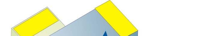
2 Outline. Measurement technique Lateral Spin-Valve Spin Hall Effect FM2 V- FM1 FM2 FM1 V- I- I- I+ V+ V+ I+ SOV, Int. J. Mod. Phys. B 23, 2413 (2009)
3 Nonlocal Spin Detection and the Spin Hall Effect Introduction Nonlocal Spin Detection, Lateral Spin-Valve Spin Hall Effect Nonlocal Electrical Detection of the Spin-Current Induced Hall Effect. Reverse Spin Hall Effect. Comparison with Lateral Spin-Valve Conclusions
4 Nonlocal Spin Detection and the Spin Hall Effect Introduction Nonlocal Spin Detection, Lateral Spin-Valve Spin Hall Effect Nonlocal Electrical Detection of the Spin-Current Induced Hall Effect. Reverse Spin Hall Effect. Comparison with Lateral Spin-Valve Conclusions
5 Nonlocal Spin Detection and the Spin Hall Effect Introduction Nonlocal Spin Detection, Lateral Spin-Valve Spin Hall Effect Nonlocal Electrical Detection of the Spin-Current Induced Hall Effect. Reverse Spin Hall Effect. Comparison with Lateral Spin-Valve Conclusions

")
6 Collaborators Lateral Spin-Valve Spin-Hall effect M. Tinkham M. Tinkham D.J. Monsma (Harvard) C.M. Marcus V. Narayanamurti aaya a ut (Harvard)


7 Nonlocal spin electronics The measured voltage depends on the relative magnetization of the ferromagnets Johnson and Silsbee (1985); Aronov (1976)
; 180 μm (37K) Jedema et al (Nature( 416, 713 (2002)) Aluminum thin films. Much smaller volume.")
8 Nonlocal spin injection/detection Johnson and Silsbee (PRL 55, 1790 (1985)) Bulk aluminum crystal pv signal (SQUID picovoltmeter) T < 77 K Spin relaxation length ~ 450 μm (4.2K); 180 μm (37K) Jedema et al (Nature( 416, 713 (2002)) Aluminum thin films. Much smaller volume. Tunnel barriers Signal 6 order of magnitude larger than Johnson V/I ~ 10 mω Reduced sample size and improved spin injection V/I ~1Ω Spin relaxation length ~0.2-1 μm (42K);0205μm ( (RT)


9 Device fabrication PMMA MMA Si/SiO 2 MMA/PMMA bilayer e-beam lithography. Large undercut by preferentially exposing more sensitive MMA Free-standing PMMA mask SOV and M. Tinkham, APL 85, 5914 (2004)


10 Device fabrication PMMA MMA Si/SiO 2 MMA/PMMA bilayer e-beam lithography. Large undercut by preferentially exposing more sensitive MMA Free-standing PMMA mask SOV and M. Tinkham, APL 85, 5914 (2004)
11 Device fabrication PMMA MMA Si/SiO 2 MMA/PMMA bilayer e-beam lithography. Large undercut by preferentially exposing more sensitive MMA Free-standing PMMA mask SOV and M. Tinkham, APL 85, 5914 (2004)


 Ferromagnet with")


12 Device fabrication e-beam evaporation. Tunnel barriers between FM and Aluminum in situ (without breaking vacuum) Ferromagnet with intrinsically different coercive field (NiFe and CoFe) and different thicknesses. NiFe Al CoFe O 2 ; Rotate Rotate
")
 The detector (NiFe) samples the")

13 Measurement scheme Current I injected into Al strip from one of the ferromagnets (CoFe) Non-equilibrium spin density (spin accumulation) The detector (NiFe) samples the electrochemical potential of the spin populations 200 nm 200 nm L L is varied to obtain the spin relaxation length
 V ± =± I 1 2 λsf PCoFePNiFe e σ A Al L / λ SOV and M. Tinkham, APL 85, 5914 (2004) SOV, Int. J. Mod. Phys. B 23, 2413 (2009) sf 4K: P = (P NiFe P CoFe ) 1/2 ~25%; λ sf ~0.")
14 Spin relaxation, spin transfer through interfaces 1 4K RT L 200 nm V/I ( Ω) 0 ΔR( ( Ω) 1-1 I = 1 μa H(T) L(nm) V ± =± I 1 2 λsf PCoFePNiFe e σ A Al L / λ SOV and M. Tinkham, APL 85, 5914 (2004) SOV, Int. J. Mod. Phys. B 23, 2413 (2009) sf 4K: P = (P NiFe P CoFe ) 1/2 ~25%; λ sf ~0.2-1 μm Room T: P ~ 17%; λ sf ~ μm Spin flip time λsf = Dτ sf τ sf ~ 50ps at RT 2 σ = en D Al
15 Tunneling spin polarization di I/dV (arb. unit) P(%) Junction Resistance (Ω μm 2 ) NiFe V Al -V NiFe (mv) CoFe V Al -V CoFe (mv) P depends on the barrier transparency (oxidation time) P can be directly compared with the polarization obtained with the Meservey-Tedrow (MT) technique in the same sample P Spin Valve (4K) = (P NiFe P CoFe ) 1/2 ~ 25% P MT-NiFe (250mK) ~ 19% H= 0; 2T P MT-CoFe( (250mK) ~ 38% P MT = 27% SOV and M. Tinkham, APL 85, 5914 (2004) I.I. Mazin, PRL 83, (1999)

 p (arb.uni 0.")

 Asymmetry in the tunneling -0.5 0.")
16 Spin polarized tunneling at finite bias V S = V dc + V ac V ac ~ mv V dc < 1.5 V V dc < 0 V dc > 0 p NiFe, CoFe = g g M M + g g m m 0.8 CoFe NiFe its) p (arb.uni 0.4 p (arb. units) V dc > 0 electrons tunnel into FM V dc < 0 electrons tunnel out of FM V dc (V) Asymmetry in the tunneling V dc (V) SOV et al., PRL 94, (2005)


 Jedema et al.")
17 Spin precession H H // H H // ϕ = ω L t H t L = 2 m Polarization and diffusion characteristics from a single measurement H Johnson and Silsbee PRL 55, 1790 (1985) Jedema et al., Nature 416, 713 (2002)
18 Nonlocal measurements applications Spin transport in metals and through interfaces T. Kimura, J. Hamrle, Y. Otani, K. Tsukagoshi and Y. Aoyagi, Appl. Phys. Lett. 85, 3501 (2004). Y. Ji, A. Hoffmann, J.S. Jiang, S.D. Bader, Appl. Phys. Lett. 85, 6218 (2004). S. Garzon, I. Zutic, and R.A. Webb, Phys. Rev. Lett. 94, (2005). Y. Ji, A. Hoffmann, J.E. Pearson, and S.D. Bader, Appl. Phys. Lett. 88, (2006). R. Godfrey and M. Johnson, Phys. Rev. Lett. 96,, (2006). J.H. Ku, J. Chang, K. Kim, and J. Eom, Appl. Phys. Lett. 88, (2006). N. Poli, M. Urech, V. Korenivski, and D.B. Haviland, J. Appl. Phys. 99, 08H701 (2006). Zero dimensional structures M. Zaffalon, and B.J. van Wees, Phys. Rev. Lett. 91, (2003). Superconductors D. Beckmann, H.B. Weber, and H.v. Löhneysen, Phys. Rev. Lett. 93, (2004). M. Urech, J. Johansson, N. Poli, V. Korenivski, and D.B. Haviland, J. Appl. Phys. 99, 08M513 (2006). Semiconductors X. Lou et al. cond-mat/ , Nat. Phys. 3, 197 (2007). Nanotubes/Graphene N. Tombros, S.J. van der Molen, and B.J. van Wees, Phys. Rev. B 73, (2006). N. Tombros et al. Nature 448, 571 (2007). Spin torque by pure spin currents T. Kimura et al., Nature Phys. 4, 11 (2008). Review S.O. Valenzuela, Int. J. Mod. Phys. B 23, 2413 (2009).
19 Spin Dynamics in Metallic Nanostructures Introduction Nonlocal Spin Detection, Lateral Spin-Valve Spin Hall Effect Nonlocal Electrical Detection of the Reverse Spin Hall Effect Comparison with Lateral Spin-Valve Conclusions
20 Spin Hall effect Spin current generation and spin accumulation without magnetic fields or ferromagnets Hall effect Spin Hall effect M.I. Dyakonov & V.I. Perel, JETP Lett. 13, 467 (1971); J.E. Hirsch, PRL 83, 1834 (1999); S Zhang PRL (2000); S Murakami N Nagaosa S C & Zhang Science 301 S. Zhang, PRL 85, 393 (2000); S. Murakami, N. Nagaosa, S.C. & Zhang. Science 301, 1348 (2003); J. Sinova, et al., PRL 92, (2004).


.")
![-1-300 0 300 H FM [Oe]](/docs-images/83/88950599/images/21-5.jpg "Spin accumulation in PM")
21 Spin Hall effect I FM PM ΔR [10-4 Oh hm] 1 0 Y.K. Kato et al. Science 306, 1910 (2004); J. Wunderlich, et al. PRL 94, (2005). V. Sih et al. Nature Physics 1, 31 (2005) H FM [Oe] Spin accumulation in PM detected with FM Experimental artifacts? S. Zhang PRL (2000).
. A.A. Bakun et al., Sov. Phys.")


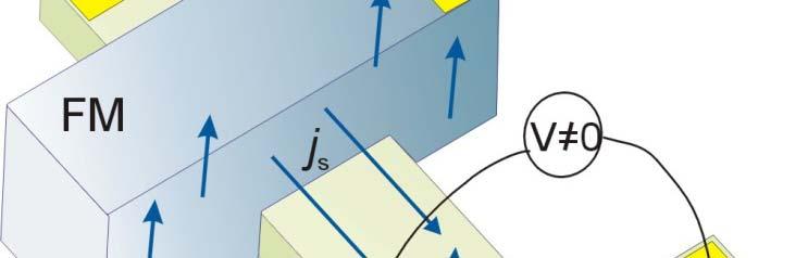
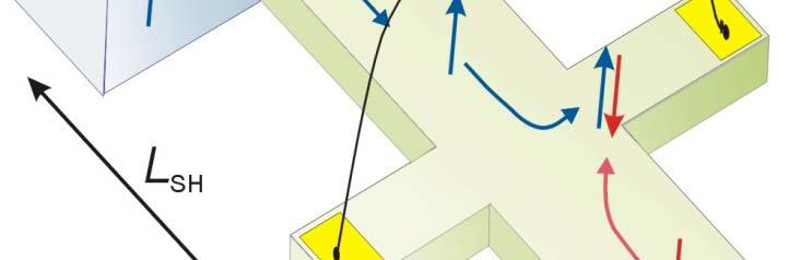
22 Spin Hall effect. Electronic detection J.E. Hirsch. PRL 83, 1834 (1999). A.A. Bakun et al., Sov. Phys. JETP Lett. 40, 1293 (1984). A current generates a spin imbalance trough the spin Hall effect in an Al strip The spin imbalance drives a spin current which generates a voltage in a second Al strip Second order effect


23 Spin Hall effect. Electronic detection


;")


24 Spin Hall effect. Electronic detection Diffusive system Charge current in y direction is zero z y and x Zhang, S. PRL 85, 393 (2000); JAP 89, 7564 (2001). S. Takahashi et al., Chapter 8 in Concepts in spin electronics (Oxford Univ. Press, 2006).


25 Sample layout CoFe e-beam lithography Shadow evaporation CoFe Al Film Al 2 O 3 tunnel barrier CoFe electrodes P ~ 30 % Al / Al 2 O 3
26 Measurement schemes Johnson-Silsbee Spin Hall effect FM1 FM2 V- FM1 FM2 V- I- I- I+ V+ V+ I+ SOV and M. Tinkham, Nature 442, 176 (2006); Int. J. Mod. Phys. B 23, 2413 (2009).


 10")


27 Nonlocal spin detection. Spin precession Jonhson-Silsbee I- FM1 FM2 V- I+ V+ ΔR R (mω) λ sf = 705 nm λ sf = 455 nm t Al = 12 nm ; t Al = 25 nm L FM (μm)
cos θ + sin 2 2 = f(")

28 Jonhson-Silsbee V V V V 0 0 =+ f( B )cos θ + sin 2 2 = f( B )cos θ + sin 2 2 θ θ Jedema et al., Nature 416, 713 (2002)
 ΔR SH sinθ ΔR SH =")
 S.")

29 Spin Hall effect V- FM1 FM2 I- V+ I+ V/I = R SH = (1/2) ΔR SH sinθ ΔR SH = 2(P σ SH / t Al σ 2 c)exp[-l SH /λ sf ] Zhang, S. PRL 85, 393 (2000) S. Takahashi et al., Chapter 8 in Concepts in spin electronics (Oxford Univ. Press, 2006)
30 Spin Hall effect V/I = R SH = (1/2) ΔR SH sinθ R SH (m mω) nm 0-1 sin θ ΔR SH = 2(P σ SH / t Al σ 2 c) exp[-l SH /λ sf ] 0.4 L SH = 480 nm SH (mω) R S nm sin θ ΔR SH (mω) θ M H H(T) 0 π/4 Angle (rad) π/2 SOV and M. Tinkham, Nature 442, 176 (2006), J. Appl. Phys. 101, 09B103 (2007)
31 Spin Hall effect Comparison with standard nonlocal detection 1 ΔR (mω Ω) λ 10 sf = 705 nm 1 λ sf = 455 nm 0.1 t Al = 12 nm ; t Al = 25 nm L FM (μm) ΔR(mΩ Ω) t = 12 nm Al t Al = 25 nm λ sf = 490 nm λ sf = 735 nm L SH (μm) ΔR SH = 2(P σ SH / t Al σ 2 c) exp[-l SH /λ sf ] σ SH ~ 30 (Wcm) -1 P ~ 28 % Predicted (extrinsic): σ ~ (cm) -1 SH 10 (Wcm) Zhang, PRL (2001); Shchelushkin & Brataas, PRB (2005) T. Kimura et al., cond-mat/ , PRL 2007


 T.")

32 Spin Hall effect Spin Hall cross adapted for materials with short spin relaxation length E. Saitoh et al., APL 88, (2006) T. Kimura et al., PRL 98, (2007) T. Seki et al., Nat. Mat. (2008)
33 Al Conclusions Electronic detection of the (reverse) spin Hall effect in a diffusive conductor. Results are consistent with those obtained with control Lateral Spin-Valves. Spin precession experiments and magnetization orientation dependence of the spin Hall effect. -1 R SH (mω) R SH (mω) nm sin θ sin θ ΔR SH (m mω) L SH = 480 nm 480 nm π/4 π/2 H(T) Angle (rad) Spin relaxation length in films with different thickness. ΔR (mω) λ 10 sf = 705 nm 1 λ sf = 455 nm 0.1 t Al = 12 nm ; t Al = 25 nm L FM (μm) ΔR(mΩ) λ sf = 490 nm λ sf = 735 nm t Al = 12 nm t Al = 25 nm L SH (μm) Theoretical estimations using -like scattering centers are in agreement with experimental results, σ SH ~ 30 (Wcm) -1. SH
Fabrication and Measurement of Spin Devices. Purdue Birck Presentation
 Fabrication and Measurement of Spin Devices Zhihong Chen School of Electrical and Computer Engineering Birck Nanotechnology Center, Discovery Park Purdue University Purdue Birck Presentation zhchen@purdue.edu
All-electrical measurements of direct spin Hall effect in GaAs with Esaki diode electrodes.
 All-electrical measurements of direct spin Hall effect in GaAs with Esaki diode electrodes. M. Ehlert 1, C. Song 1,2, M. Ciorga 1,*, M. Utz 1, D. Schuh 1, D. Bougeard 1, and D. Weiss 1 1 Institute of Experimental
Nonlocal electrical detection of spin accumulation. generated by Anomalous Hall effects in mesoscopic. Ni 81 Fe 19 films
 Nonlocal electrical detection of spin accumulation generated by Anomalous Hall effects in mesoscopic Ni 81 Fe 19 films Chuan Qin, Shuhan Chen, * Yunjiao Cai, Fatih Kandaz, and Yi Ji Department of Physics
Spin relaxation of conduction electrons Jaroslav Fabian (Institute for Theoretical Physics, Uni. Regensburg)
") Spin relaxation of conduction electrons Jaroslav Fabian (Institute for Theoretical Physics, Uni. Regensburg) :Syllabus: 1. Introductory description 2. Elliott-Yafet spin relaxation and spin hot spots 3.
Spin relaxation of conduction electrons Jaroslav Fabian (Institute for Theoretical Physics, Uni. Regensburg) :Syllabus: 1. Introductory description 2. Elliott-Yafet spin relaxation and spin hot spots 3.
Expecting the unexpected in the spin Hall effect: from fundamental to practical
 Expecting the unexpected in the spin Hall effect: from fundamental to practical JAIRO SINOVA Texas A&M University Institute of Physics ASCR Institute of Physics ASCR Tomas Jungwirth, Vít Novák, et al Hitachi
Recent developments in spintronic
 Recent developments in spintronic Tomas Jungwirth nstitute of Physics ASCR, Prague University of Nottingham in collaboration with Hitachi Cambridge, University of Texas, Texas A&M University - Spintronics
Spin Funneling for Enhanced Spin Injection into Ferromagnets: Supplementary Information
 Spin Funneling for Enhanced Spin Injection into Ferromagnets: Supplementary Information Shehrin Sayed, Vinh Q. Diep, Kerem Yunus Camsari, and Supriyo Datta School of Electrical and Computer Engineering,
Magnon-drag thermopile
 Magnon-drag thermopile I. DEVICE FABRICATION AND CHARACTERIZATION Our devices consist of a large number of pairs of permalloy (NiFe) wires (30 nm wide, 20 nm thick and 5 µm long) connected in a zigzag
Saroj P. Dash. Chalmers University of Technology. Göteborg, Sweden. Microtechnology and Nanoscience-MC2
 Silicon Spintronics Saroj P. Dash Chalmers University of Technology Microtechnology and Nanoscience-MC2 Göteborg, Sweden Acknowledgement Nth Netherlands University of Technology Sweden Mr. A. Dankert Dr.
Room-Temperature Electron Spin Transport in a Highly Doped Si Channel. AIT, Akita Research Institute of Advanced Technology, Akita , Japan
 Room-Temperature Electron Spin Transport in a Highly Doped Si Channel Toshio Suzuki*, Tomoyuki Sasaki 1, Tohru Oikawa 1, Masashi Shiraishi, Yoshishige Suzuki, and Kiyoshi Noguchi 1 AIT, Akita Research
Spin orbit interaction induced spin-separation in platinum nanostructures
 Spin orbit interaction induced spin-separation in platinum nanostructures Koong Chee Weng 1,2, N. Chandrasekhar 1,2, Christian Miniatura 1,3 Berthold-Georg Englert 1,4 1 Department of Physics, National
Spin injection, accumulation, and precession in a mesoscopic nonmagnetic metal island Zaffalon, M; van Wees, Bart
 University of Groningen Spin injection, accumulation, and precession in a mesoscopic nonmagnetic metal island Zaffalon, M; van Wees, Bart Published in: Physical Review. B: Condensed Matter and Materials
Physics and applications (I)
") Spintronics: Physics and applications (I) Malek Zareyan IPM, 15 TiR 1387 1 Very weak magnetic changes give rise to major differences in resistance in a GMR system (.( ١٩٨٨ GMR has made possible miniaturizing
Spintronics: Physics and applications (I) Malek Zareyan IPM, 15 TiR 1387 1 Very weak magnetic changes give rise to major differences in resistance in a GMR system (.( ١٩٨٨ GMR has made possible miniaturizing
Spin injection and the local Hall effect in InAs quantum wells
 Spin injection and the local Hall effect in InAs quantum wells F.G. Monzon * and M.L. Roukes California Institute of Technology, Condensed Matter Physics 114-36, Pasadena CA 91125 We report on our efforts
Spin pumping in Ferromagnet-Topological Insulator-Ferromagnet Heterostructures Supplementary Information.
 Spin pumping in Ferromagnet-Topological Insulator-Ferromagnet Heterostructures Supplementary Information. A.A. Baker,, 2 A.I. Figueroa, 2 L.J. Collins-McIntyre, G. van der Laan, 2 and T., a) Hesjedal )
Temperature dependence of spin diffusion length in silicon by Hanle-type spin. precession
 Temperature dependence of spin diffusion length in silicon by Hanle-type spin precession T. Sasaki 1,a), T. Oikawa 1, T. Suzuki 2, M. Shiraishi 3, Y. Suzuki 3, and K. Noguchi 1 SQ Research Center, TDK
Observation of the intrinsic inverse spin Hall effect in Ni 80 Fe 20. Yuichiro Ando, Teruya Shinjo and Masashi Shiraishi * #
 Observation of the intrinsic inverse spin Hall effect in Ni 80 Fe 20 Ayaka Tsukahara #, Yuta Kitamura #, Eiji Shikoh, Yuichiro Ando, Teruya Shinjo and Masashi Shiraishi * # Graduate School of Engineering
Spin transport in graphene - hexagonal boron nitride van der Waals heterostructures Gurram, Mallikarjuna
 University of Groningen Spin transport in graphene - hexagonal boron nitride van der Waals heterostructures Gurram, Mallikarjuna IMPORTANT NOTE: You are advised to consult the publisher's version (publisher's
Spatiotemporal magnetic imaging at the nanometer and picosecond scales
 AFOSR Nanoelectronics Review, Oct. 24, 2016 Spatiotemporal magnetic imaging at the nanometer and picosecond scales Gregory D. Fuchs School of Applied & Engineering Physics, Cornell University T M V TRANE
ConceptGraphene. Small or medium-scale focused research project. WP4 Spin transport devices
 ConceptGraphene New Electronics Concept: Wafer-Scale Epitaxial Graphene Small or medium-scale focused research project WP4 Spin transport devices Deliverable 4.1 Report on spin transport in graphene on
Mesoscopic Spintronics
 Mesoscopic Spintronics Taro WAKAMURA (Université Paris-Sud) Lecture 1 Today s Topics 1.1 History of Spintronics 1.2 Fudamentals in Spintronics Spin-dependent transport GMR and TMR effect Spin injection
Focused-ion-beam milling based nanostencil mask fabrication for spin transfer torque studies. Güntherodt
 Focused-ion-beam milling based nanostencil mask fabrication for spin transfer torque studies B. Özyilmaz a, G. Richter, N. Müsgens, M. Fraune, M. Hawraneck, B. Beschoten b, and G. Güntherodt Physikalisches
Spin Injection into a Graphene Thin Film at Room Temperature
 Spin Injection into a Graphene Thin Film at Room Temperature Megumi Ohishi, Masashi Shiraishi*, Ryo Nouchi, Takayuki Nozaki, Teruya Shinjo, and Yoshishige Suzuki Graduate School of Engineering Science,
Spin injection. concept and technology
 Spin injection concept and technology Ron Jansen ャンセンロン Spintronics Research Center National Institute of Advanced Industrial Science and Technology (AIST), Tsukuba, Japan Spin injection Transfer of spin
United Nations Educational, Scientific and Cultural Organization and International Atomic Energy Agency
 Available at: http://publications.ictp.it IC/2010/033 United Nations Educational, Scientific and Cultural Organization and International Atomic Energy Agency THE ABDUS SALAM INTERNATIONAL CENTRE FOR THEORETICAL
Fundamental concepts of spintronics
 Fundamental concepts of spintronics Jaroslav Fabian Institute for Theoretical Physics University of Regensburg Stara Lesna, 24. 8. 2008 SFB 689 :outline: what is spintronics? spin injection spin-orbit
Spin Currents in a 2D Electron Gas
 Spin Currents in a 2D Electron Gas Joshua Folk UBC Asilomar, 2007 Thanks to: My group Sergey Frolov (postdoc) Ananth Venkatesan (postdoc) Mark Lundeberg (PhD) Wing Wa Yu (Masters) Yuan Ren (Masters) Chung-Yu
Effect of anisotropic spin absorption on the Hanle effect in lateral spin valves
 SUPPLEMETARY IFORMATIO Effect of anisotropic spin absorption on the Hanle effect in lateral spin valves H. Idzuchi,*, Y. Fuuma,3, S. Taahashi 4,5, S. Maeawa 5,6 and Y. Otani,* Institute for Solid State
Current-driven ferromagnetic resonance, mechanical torques and rotary motion in magnetic nanostructures
 Current-driven ferromagnetic resonance, mechanical torques and rotary motion in magnetic nanostructures Alexey A. Kovalev Collaborators: errit E.W. Bauer Arne Brataas Jairo Sinova In the first part of
Supplementary material: Nature Nanotechnology NNANO D
 Supplementary material: Nature Nanotechnology NNANO-06070281D Coercivities of the Co and Ni layers in the nanowire spin valves In the tri-layered structures used in this work, it is unfortunately not possible
Optical studies of current-induced magnetization
 Optical studies of current-induced magnetization Virginia (Gina) Lorenz Department of Physics, University of Illinois at Urbana-Champaign PHYS403, December 5, 2017 The scaling of electronics John Bardeen,
Spin Hall and quantum spin Hall effects. Shuichi Murakami Department of Physics, Tokyo Institute of Technology PRESTO, JST
 YKIS2007 (Kyoto) Nov.16, 2007 Spin Hall and quantum spin Hall effects Shuichi Murakami Department of Physics, Tokyo Institute of Technology PRESTO, JST Introduction Spin Hall effect spin Hall effect in
arxiv: v3 [cond-mat.mtrl-sci] 11 Aug 2008
![arxiv: v3 [cond-mat.mtrl-sci] 11 Aug 2008](/thumbs/71/65777543.jpg "arxiv: v3 [cond-mat.mtrl-sci] 11 Aug 2008") Non-ohmic spin transport in n-type doped silicon Hyuk-Jae Jang, Jing Xu, Jing Li, Biqin Huang, and Ian Appelbaum Department of Electrical and Computer Engineering, University of Delaware, Newark, Delaware,
Non-ohmic spin transport in n-type doped silicon Hyuk-Jae Jang, Jing Xu, Jing Li, Biqin Huang, and Ian Appelbaum Department of Electrical and Computer Engineering, University of Delaware, Newark, Delaware,
An Overview of Spintronics in 2D Materials
 An Overview of Spintronics in 2D Materials Wei Han ( 韩伟 ) 1 2014 ICQM Outline I. Introduction to spintronics (Lecture I) II. Spin injection and detection in 2D (Lecture I) III. Putting magnetic moment
arxiv: v1 [cond-mat.mes-hall] 13 Sep 2016
![arxiv: v1 [cond-mat.mes-hall] 13 Sep 2016](/thumbs/89/99022139.jpg "arxiv: v1 [cond-mat.mes-hall] 13 Sep 2016") Conditions for the generation of spin currents in spin-hall devices.-e. Wegrowe 1, R. V. Benda 1,2, and. M. Rubì 2 1 Ecole Polytechnique, LSI, CNRS and CEA/DSM/IRAMIS, Palaiseau F-91128, France and 2 Departament
Conditions for the generation of spin currents in spin-hall devices.-e. Wegrowe 1, R. V. Benda 1,2, and. M. Rubì 2 1 Ecole Polytechnique, LSI, CNRS and CEA/DSM/IRAMIS, Palaiseau F-91128, France and 2 Departament
Lecture I. Spin Orbitronics
 Lecture I Spin Orbitronics Alireza Qaiumzadeh Radboud University (RU) Institute for Molecules and Materials (IMM) Theory of Condensed Matter group (TCM) What We Talk About When We Talk About Spin Orbitronics
Molecular Spintronics using -Electron Molecules
 2008.12.18 TU-Dresden Molecular Spintronics using -Electron Molecules Masashi Shiraishi 1. Osaka University, Japan. 2. JST-PRESTO, Japan Co-workers in this study Osaka University Prof. Yoshishige Suzuki
Electrical detection of spin transport in lateral ferromagnet semiconductor devices
 Electrical detection of spin transport in lateral ferromagnet semiconductor devices XIAOHUA LOU 1, CHRISTOPH ADELMANN 2, SCOTT A. CROOKER 3,ERICS.GARLID 1, JIANJIE ZHANG 1, K. S. MADHUKAR REDDY 2, SOREN
Systèmes Hybrides. Norman Birge Michigan State University
 Systèmes Hybrides Norman Birge Michigan State University Résumé Systèmes F/N Systèmes S/N Systèmes S/F Résumé: Systèmes F/N Accumulation de spin Giant Magnetoresistance (GMR) Spin-transfer torque (STT)
Magnetic oscillations driven by the spin Hall effect in 3-terminal magnetic tunnel junction. devices. Cornell University, Ithaca, NY 14853
 Magnetic oscillations driven by the spin Hall ect in 3-terminal magnetic tunnel junction devices Luqiao Liu 1, Chi-Feng Pai 1, D. C. Ralph 1,2, R. A. Buhrman 1 1 Cornell University, Ithaca, NY 14853 2
Theory of electrical spin injection: Tunnel contacts as a solution of the conductivity mismatch problem
 Theory of electrical spin injection: Tunnel contacts as a solution of the conductivity mismatch problem The Harvard community has made this article openly available. Please share how this access benefits
Transient grating measurements of spin diffusion. Joe Orenstein UC Berkeley and Lawrence Berkeley National Lab
 Transient grating measurements of spin diffusion Joe Orenstein UC Berkeley and Lawrence Berkeley National Lab LBNL, UC Berkeley and UCSB collaboration Chris Weber, Nuh Gedik, Joel Moore, JO UC Berkeley
GMR Read head. Eric Fullerton ECE, CMRR. Introduction to recording Basic GMR sensor Next generation heads TMR, CPP-GMR UCT) Challenges ATE
 Challenges ATE") GMR Read head Eric Fullerton ECE, CMRR Introduction to recording Basic GMR sensor Next generation heads TMR, CPP-GMR UCT) Challenges ATE 1 Product scaling 5 Mbyte 100 Gbyte mobile drive 8 Gbyte UCT) ATE
GMR Read head Eric Fullerton ECE, CMRR Introduction to recording Basic GMR sensor Next generation heads TMR, CPP-GMR UCT) Challenges ATE 1 Product scaling 5 Mbyte 100 Gbyte mobile drive 8 Gbyte UCT) ATE
arxiv: v1 [cond-mat.mes-hall] 19 Dec 2008
![arxiv: v1 [cond-mat.mes-hall] 19 Dec 2008](/thumbs/72/67207946.jpg "arxiv: v1 [cond-mat.mes-hall] 19 Dec 2008") Ballistic Intrinsic Spin-Hall Effect in HgTe Nanostructures C. Brüne 1, A. Roth 1, E.G. Novik 1, M. König 1, H. Buhmann 1, E.M. Hankiewicz, W. Hanke, J. Sinova 3, and L. W. Molenkamp 1 1 Physikalisches
Ballistic Intrinsic Spin-Hall Effect in HgTe Nanostructures C. Brüne 1, A. Roth 1, E.G. Novik 1, M. König 1, H. Buhmann 1, E.M. Hankiewicz, W. Hanke, J. Sinova 3, and L. W. Molenkamp 1 1 Physikalisches
arxiv:cond-mat/ v1 [cond-mat.mes-hall] 28 Apr 2006
![arxiv:cond-mat/ v1 [cond-mat.mes-hall] 28 Apr 2006](/thumbs/71/65742769.jpg "arxiv:cond-mat/ v1 [cond-mat.mes-hall] 28 Apr 2006") The Magneto-coulomb effect in spin valve devices S.J. van der Molen, 1 N. Tombros, 1 and B.J. van Wees 1 arxiv:cond-mat/0604654v1 [cond-mat.mes-hall] 28 Apr 2006 1 Physics of Nanodevices, Materials Science
The Magneto-coulomb effect in spin valve devices S.J. van der Molen, 1 N. Tombros, 1 and B.J. van Wees 1 arxiv:cond-mat/0604654v1 [cond-mat.mes-hall] 28 Apr 2006 1 Physics of Nanodevices, Materials Science
Observation of the intrinsic inverse spin Hall effect from ferromagnet
 Observation of the intrinsic inverse spin Hall effect from ferromagnet Ayaka Tsukahara #, Yuta Kitamura #, Eiji Shikoh, Yuichiro Ando, Teruya Shinjo and Masashi Shiraishi * # Graduate School of Engineering
Citation for published version (APA): Filip, A. T. (2002). Spin polarized electron transport in mesoscopic hybrid devices s.n.
: Filip, A. T. (2002). Spin polarized electron transport in mesoscopic hybrid devices s.n.") University of Groningen Spin polarized electron transport in mesoscopic hybrid devices Filip, Andrei Teodor IMPORTANT NOTE: You are advised to consult the publisher's version (publisher's PDF) if you wish
University of Groningen Spin polarized electron transport in mesoscopic hybrid devices Filip, Andrei Teodor IMPORTANT NOTE: You are advised to consult the publisher's version (publisher's PDF) if you wish
Abstract. I. Introduction
 Temperature dependence of spin diffusion length and spin Hall angle in Au and Pt Miren Isasa 1, Estitxu Villamor 1, Luis E. Hueso 1,2, Martin Gradhand 3 and Fèlix Casanova 1,2 1 CIC nanogune, 20018 Donostia-San
Enhancement of spin relaxation time in hydrogenated graphene spin-valve devices Wojtaszek, M.; Vera-Marun, I. J.; Maassen, T.
 University of Groningen Enhancement of spin relaxation time in hydrogenated graphene spin-valve devices Wojtaszek, M.; Vera-Marun, I. J.; Maassen, T.; van Wees, Bart Published in: Physical Review. B: Condensed
Long distance transport of magnon spin information in a magnetic insulator at room temperature
 Long distance transport of magnon spin information in a magnetic insulator at room temperature L.J. Cornelissen 1 *, J.Liu 1, R.A. Duine 2, J. Ben Youssef 3 & B. J. van Wees 1 1 Zernike Institute for Advanced
(Spain) * 1 CIC nanogune, Donostia-San Sebastian, Basque Country (Spain)
 * 1 CIC nanogune, Donostia-San Sebastian, Basque Country (Spain)") Temperature dependence of spin polarization in ferromagnetic metals using lateral spin valves Estitxu Villamor, 1 Miren Isasa, 1 Luis E. Hueso, 1,2 and Fèlix Casanova 1,2 * 1 CIC nanogune, 20018 Donostia-San
Temperature dependence of spin polarization in ferromagnetic metals using lateral spin valves Estitxu Villamor, 1 Miren Isasa, 1 Luis E. Hueso, 1,2 and Fèlix Casanova 1,2 * 1 CIC nanogune, 20018 Donostia-San
Experimental discovery of the spin-hall effect in Rashba spin-orbit coupled semiconductor systems
 Experimental discovery of the spin-hall effect in Rashba spin-orbit coupled semiconductor systems J. Wunderlich, 1 B. Kästner, 1,2 J. Sinova, 3 T. Jungwirth 4,5 1 Hitachi Cambridge Laboratory, Cambridge
Transport through Andreev Bound States in a Superconductor-Quantum Dot-Graphene System
 Transport through Andreev Bound States in a Superconductor-Quantum Dot-Graphene System Nadya Mason Travis Dirk, Yung-Fu Chen, Cesar Chialvo Taylor Hughes, Siddhartha Lal, Bruno Uchoa Paul Goldbart University
Spin orbit torque driven magnetic switching and memory. Debanjan Bhowmik
 Spin orbit torque driven magnetic switching and memory Debanjan Bhowmik Spin Transfer Torque Fixed Layer Free Layer Fixed Layer Free Layer Current coming out of the fixed layer (F2) is spin polarized in
MSE 7025 Magnetic Materials (and Spintronics)
") MSE 7025 Magnetic Materials (and Spintronics) Lecture 14: Spin Transfer Torque And the future of spintronics research Chi-Feng Pai cfpai@ntu.edu.tw Course Outline Time Table Week Date Lecture 1 Feb 24
MSE 7025 Magnetic Materials (and Spintronics) Lecture 14: Spin Transfer Torque And the future of spintronics research Chi-Feng Pai cfpai@ntu.edu.tw Course Outline Time Table Week Date Lecture 1 Feb 24
Current-driven Magnetization Reversal in a Ferromagnetic Semiconductor. (Ga,Mn)As/GaAs/(Ga,Mn)As Tunnel Junction
As/GaAs/(Ga,Mn)As Tunnel Junction") Current-driven Magnetization Reversal in a Ferromagnetic Semiconductor (Ga,Mn)As/GaAs/(Ga,Mn)As Tunnel Junction D. Chiba 1, 2*, Y. Sato 1, T. Kita 2, 1, F. Matsukura 1, 2, and H. Ohno 1, 2 1 Laboratory
Current-driven Magnetization Reversal in a Ferromagnetic Semiconductor (Ga,Mn)As/GaAs/(Ga,Mn)As Tunnel Junction D. Chiba 1, 2*, Y. Sato 1, T. Kita 2, 1, F. Matsukura 1, 2, and H. Ohno 1, 2 1 Laboratory
MAGNETORESISTANCE PHENOMENA IN MAGNETIC MATERIALS AND DEVICES. J. M. De Teresa
 MAGNETORESISTANCE PHENOMENA IN MAGNETIC MATERIALS AND DEVICES J. M. De Teresa Instituto de Ciencia de Materiales de Aragón, Universidad de Zaragoza-CSIC, Facultad de Ciencias, 50009 Zaragoza, Spain. E-mail:
LECTURE 3: Refrigeration
 LECTURE 3: Refrigeration Refrigeration on-chip Thermoelectric refrigeration Peltier refrigerators, Peltier 1834 Thermionic refrigeration, Mahan, 1994 Korotkov and Likharev, 1999 Quantum-dot refrigerator,
The contribution of hot-electron spin polarization to the spin-dependent magnetotransport in a spin-valve transistor at finite temperatures
 INSTITUTE OF PHYSICS PUBLISHING JOURNAL OF PHYSICS: CONDENSED MATTER J. Phys.: Condens. Matter 14 (2002 865 872 PII: S0953-8984(0228168-0 The contribution of hot-electron spin polarization to the spin-dependent
Spin transport in graphene - hexagonal boron nitride van der Waals heterostructures Gurram, Mallikarjuna
 University of Groningen Spin transport in graphene - hexagonal boron nitride van der Waals heterostructures Gurram, Mallikarjuna IMPORTANT NOTE: You are advised to consult the publisher's version (publisher's
arxiv:cond-mat/ v1 [cond-mat.mes-hall] 3 Feb 1999
![arxiv:cond-mat/ v1 [cond-mat.mes-hall] 3 Feb 1999](/thumbs/88/117721611.jpg "arxiv:cond-mat/ v1 [cond-mat.mes-hall] 3 Feb 1999") An observation of spin-valve effects in a semiconductor field effect transistor: a novel spintronic device. arxiv:cond-mat/99257v1 [cond-mat.mes-hall] 3 Feb 1999 S. Gardelis, C.G Smith, C.H.W. Barnes,
An observation of spin-valve effects in a semiconductor field effect transistor: a novel spintronic device. arxiv:cond-mat/99257v1 [cond-mat.mes-hall] 3 Feb 1999 S. Gardelis, C.G Smith, C.H.W. Barnes,
Electron spins in nonmagnetic semiconductors
 Electron spins in nonmagnetic semiconductors Yuichiro K. Kato Institute of Engineering Innovation, The University of Tokyo Physics of non-interacting spins Optical spin injection and detection Spin manipulation
Spin-dependent tunneling through organic molecules: spin scattering by organic radicals
 Spin-dependent tunneling through organic molecules: spin scattering by organic radicals P. LeClair Physics & Astronomy, MINT, University of Alabama G.J. Szulczewski, A. Gupta, S. Street Weihao Xu Chemistry,
Spintronic device structures
 Spintech V Krakow 7.7.2009 Spintronic device structures Jaroslav Fabian Institute for Theoretical Physics University of Regensburg Giant Magnetoresistance (GMR) magnetoelectronics Tunneling Magnetoresistance
Spin Seebeck insulator
 Spin Seebeck insulator K. Uchida 1, J. Xiao 2,3, H. Adachi 4,5, J. Ohe 4,5, S. Takahashi 1,5, J. Ieda 4,5, T. Ota 1, Y. Kajiwara 1, H. Umezawa 6, H. Kawai 6, G. E. W. Bauer 3, S. Maekawa 4,5 and E. Saitoh
arxiv: v1 [cond-mat.mtrl-sci] 28 Jul 2008
![arxiv: v1 [cond-mat.mtrl-sci] 28 Jul 2008](/thumbs/88/117898456.jpg "arxiv: v1 [cond-mat.mtrl-sci] 28 Jul 2008") Current induced resistance change of magnetic tunnel junctions with ultra-thin MgO tunnel barriers Patryk Krzysteczko, 1, Xinli Kou, 2 Karsten Rott, 1 Andy Thomas, 1 and Günter Reiss 1 1 Bielefeld University,
Current induced resistance change of magnetic tunnel junctions with ultra-thin MgO tunnel barriers Patryk Krzysteczko, 1, Xinli Kou, 2 Karsten Rott, 1 Andy Thomas, 1 and Günter Reiss 1 1 Bielefeld University,
CURRENT-INDUCED MAGNETIC DYNAMICS IN NANOSYSTEMS
 CURRENT-INDUCED MAGNETIC DYNAMICS IN NANOSYSTEMS J. Barna Department of Physics Adam Mickiewicz University & Institute of Molecular Physics, Pozna, Poland In collaboration: M Misiorny, I Weymann, AM University,
SUPPLEMENTARY INFORMATION
 Quasiparticle-mediated spin Hall effect in a superconductor T. Wakamura 1, H. Akaike 2, Y. Omori 1, Y. Niimi 1, S. Takahashi 3, A. Fujimaki 2, S. Maekawa 4,5 and YoshiChika Otani 1,6 1 Institute for Solid
Electric power transfer in spin pumping experiments
 Electric power transfer in spin pumping experiments K. Rogdakis 1, N. Alfert 1, A. Srivastava 2, J.W.A. Robinson 2, M. G. Blamire 2, L. F. Cohen 3, and H. Kurebayashi 1,a) 1 London Centre for Nanotechnology,
Electrical spin injection and detection of spin precession in room temperature bulk GaN lateral spin valves
 Electrical spin injection and detection of spin precession in room temperature bulk GaN lateral spin valves Aniruddha Bhattacharya a), Md Zunaid Baten a) and Pallab Bhattacharya a) a) Center for Photonic
SPINTRONICS. Waltraud Buchenberg. Faculty of Physics Albert-Ludwigs-University Freiburg
 SPINTRONICS Waltraud Buchenberg Faculty of Physics Albert-Ludwigs-University Freiburg July 14, 2010 TABLE OF CONTENTS 1 WHAT IS SPINTRONICS? 2 MAGNETO-RESISTANCE STONER MODEL ANISOTROPIC MAGNETO-RESISTANCE
SUPPLEMENTARY INFORMATION
 UPPLEMENTARY INFORMATION doi: 0.038/nmat78. relaxation time, effective s polarization, and s accumulation in the superconducting state The s-orbit scattering of conducting electrons by impurities in metals
Lecture I. Spin Orbitronics
 Lecture I Spin Orbitronics Alireza Qaiumzadeh Radboud University (RU) Institute for Molecules and Materials (IMM) Theory of Condensed Matter group (TCM) What We Talk About When We Talk About Spin Orbitronics
Physics of Semiconductors
 Physics of Semiconductors 13 th 2016.7.11 Shingo Katsumoto Department of Physics and Institute for Solid State Physics University of Tokyo Outline today Laughlin s justification Spintronics Two current
TRANSVERSE SPIN TRANSPORT IN GRAPHENE
 International Journal of Modern Physics B Vol. 23, Nos. 12 & 13 (2009) 2641 2646 World Scientific Publishing Company TRANSVERSE SPIN TRANSPORT IN GRAPHENE TARIQ M. G. MOHIUDDIN, A. A. ZHUKOV, D. C. ELIAS,
Magnetic switching by spin torque from the spin Hall effect
 Magnetic switching by spin torque from the spin Hall effect Luqiao Liu 1, O. J. Lee 1, T. J. Gudmundsen 1, D. C. Ralph 1,2 and R. A. Buhrman 1 1 Cornell University and 2 Kavli Institute at Cornell, Ithaca,
SUPPLEMENTARY INFORMATION
 Direct observation of the spin-dependent Peltier effect J. Flipse, F. L. Bakker, A. Slachter, F. K. Dejene & B. J. van Wees A. Calculation of the temperature gradient We first derive an expression for
Electrical spin-injection into semiconductors
 Electrical spin-injection into semiconductors L. W. Molenkamp Physikalisches Institut Universität Würzburg Am Hubland 97074 Würzburg Germany Contents Motivation The usual approach Theoretical treatment
Spin-torque nano-oscillators trends and challenging
 Domain Microstructure and Dynamics in Magnetic Elements Heraklion, Crete, April 8 11, 2013 Spin-torque nano-oscillators trends and challenging N H ext S Giovanni Finocchio Department of Electronic Engineering,
Elementary Process of Electromigration at Metallic Nanojunctions in the Ballistic Regime
 Elementary Process of Electromigration at Metallic Nanojunctions in the Ballistic Regime Kaz Hirakawa Institute of Industrial Science, University of Tokyo CREST, JST collaborators: Akinori Umeno, Kenji
Superconducting fluctuations, interactions and disorder : a subtle alchemy
 Les défis actuels de la supraconductivité Dautreppe 2011 Superconducting fluctuations, interactions and disorder : a subtle alchemy Claude Chapelier, Benjamin Sacépé, Thomas Dubouchet INAC-SPSMS-LaTEQS,
Interface magnetism and spin wave scattering in ferromagnet-insulator-ferromagnet tunnel junctions Moodera, J.S.; Nowak, J.; van de Veerdonk, R.J.M.
 Interface magnetism and spin wave scattering in ferromagnet-insulator-ferromagnet tunnel junctions Moodera, J.S.; Nowak, J.; van de Veerdonk, R.J.M. Published in: Physical Review Letters DOI: 10.1103/PhysRevLett.80.2941
Dynamically-generated pure spin current in single-layer graphene
 Dynamically-generated pure spin current in single-layer graphene Zhenyao Tang 1,#, Eiji Shikoh 1,#, Hiroki Ago 2, Kenji Kawahara 2, Yuichiro Ando 1, Teruya Shinjo 1 and Masashi Shiraishi 1,* 1. Graduate
Supplementary figures
 Supplementary figures Supplementary Figure 1. A, Schematic of a Au/SRO113/SRO214 junction. A 15-nm thick SRO113 layer was etched along with 30-nm thick SRO214 substrate layer. To isolate the top Au electrodes
High-Temperature Superconductors: Playgrounds for Broken Symmetries
 High-Temperature Superconductors: Playgrounds for Broken Symmetries Gauge / Phase Reflection Time Laura H. Greene Department of Physics Frederick Seitz Materials Research Laboratory Center for Nanoscale
Citation for published version (APA): Filip, A. T. (2002). Spin polarized electron transport in mesoscopic hybrid devices s.n.
: Filip, A. T. (2002). Spin polarized electron transport in mesoscopic hybrid devices s.n.") University of Groningen Spin polarized electron transport in mesoscopic hybrid devices Filip, Andrei Teodor IMPORTANT NOTE: You are advised to consult the publisher's version (publisher's PDF) if you wish
University of Groningen Spin polarized electron transport in mesoscopic hybrid devices Filip, Andrei Teodor IMPORTANT NOTE: You are advised to consult the publisher's version (publisher's PDF) if you wish
Shuichi Murakami Department of Physics, Tokyo Institute of Technology
 EQPCM, ISSP, U. Tokyo June, 2013 Berry curvature and topological phases for magnons Shuichi Murakami Department of Physics, Tokyo Institute of Technology Collaborators: R. Shindou (Tokyo Tech. Peking Univ.)
Semiconductor Devices
 Semiconductor Devices - 2014 Lecture Course Part of SS Module PY4P03 Dr. P. Stamenov School of Physics and CRANN, Trinity College, Dublin 2, Ireland Hilary Term, TCD 17 th of Jan 14 Metal-Semiconductor
Room-temperature perpendicular magnetization switching through giant spin-orbit torque from sputtered Bi x Se (1-x) topological insulator material
 topological insulator material") Room-temperature perpendicular magnetization switching through giant spin-orbit torque from sputtered Bi x Se (1-x) topological insulator material Mahendra DC 1, Mahdi Jamali 2, Jun-Yang Chen 2, Danielle
Room-temperature perpendicular magnetization switching through giant spin-orbit torque from sputtered Bi x Se (1-x) topological insulator material Mahendra DC 1, Mahdi Jamali 2, Jun-Yang Chen 2, Danielle
Lecture 6: Spin Dynamics
 Lecture 6: Spin Dynamics All kinds of resonance spectroscopies deliver (at least) 3 informations: 1. The resonance position. The width of the resonance (and its shape) 3. The area under the resonance From
University of Groningen. Taking topological insulators for a spin de Vries, Eric Kornelis
 University of Groningen Taking topological insulators for a spin de Vries, Eric Kornelis IMPORTANT NOTE: You are advised to consult the publisher's version (publisher's PDF) if you wish to cite from it.
New Quantum Transport Results in Type-II InAs/GaSb Quantum Wells
 New Quantum Transport Results in Type-II InAs/GaSb Quantum Wells Wei Pan Sandia National Laboratories Sandia National Laboratories is a multi-program laboratory managed and operated by Sandia Corporation,
Spin currents injected electrically and thermally from highly spin polarized Co2MnSi
 Spin currents injected electrically and thermally from highly spin polarized Co2MnSi Alexander Pfeiffer, Shaojie Hu, Robert M. Reeve, Alexander Kronenberg, Martin Jourdan, Takashi Kimura, and Mathias Kläui
Electrical spin injection from ferromagnet into an InAs heterostructures through MgO tunnel barrier
 Electrical spin injection from ferromagnet into an InAs heterostructures through MgO tunnel barrier T. Ishikura, Z. Cui, L-K. Liefeith, K. Konishi and Kanji Yoh Research center for integrated quantum electronics,
Citation for published version (APA): Jedema, F. (2002). Electrical spin injection in metallic mesoscopic spin valves. Groningen: s.n.
: Jedema, F. (2002). Electrical spin injection in metallic mesoscopic spin valves. Groningen: s.n.") University of Groningen Electrical spin injection in metallic mesoscopic spin valves Jedema, Friso IMPORTANT NOTE: You are advised to consult the publisher's version (publisher's PDF) if you wish to cite
University of Groningen Electrical spin injection in metallic mesoscopic spin valves Jedema, Friso IMPORTANT NOTE: You are advised to consult the publisher's version (publisher's PDF) if you wish to cite
Spin transfer torque devices utilizing the giant spin Hall effect of tungsten
 Spin transfer torque devices utilizing the giant spin Hall effect of tungsten Chi-Feng Pai, 1,a) Luqiao Liu, 1 Y. Li, 1 H. W. Tseng, 1 D. C. Ralph 1,2 and R. A. Buhrman 1 1 Cornell University, Ithaca,
Imprinting domain/spin configurations in antiferromagnets. A way to tailor hysteresis loops in ferromagnetic-antiferromagnetic systems
 Imprinting domain/spin configurations in antiferromagnets A way to tailor hysteresis loops in ferromagnetic-antiferromagnetic systems Dr. J. Sort Institució Catalana de Recerca i Estudis Avançats (ICREA)
All-Electrical Spin Field Effect Transistor in van der Waals Heterostructures at Room Temperature
 All-Electrical Spin Field Effect Transistor in van der Waals Heterostructures at Room Temperature André Dankert*, Saroj P. Dash Department of Microtechnology and Nanoscience, Chalmers University of Technology,
Spintronics and Spin Current
 Spintronics and Spin Current Spintronics and Spin Current Shun-Qing Shen Department of Physics, The University of Hong Kong, Pokfulam Road, Hong Kong Conventional electronics completely ignores the electron
Quantum Phase Slip Junctions
 Quantum Phase Slip Junctions Joël Peguiron Insitute of Physics, University of Basel Monday Morning Meeting, 24 April 2006 1 Goal Monday Morning Meeting, 24 April 2006 2 Evidence for Thermodynamic Fluctuations